Active-matrix touchscreen
Cok J
U.S. patent number 10,170,535 [Application Number 15/705,810] was granted by the patent office on 2019-01-01 for active-matrix touchscreen. This patent grant is currently assigned to X-Celeprint Limited. The grantee listed for this patent is X-Celeprint Limited. Invention is credited to Ronald S. Cok.


| United States Patent | 10,170,535 |
| Cok | January 1, 2019 |
Active-matrix touchscreen
Abstract
An active-matrix touchscreen includes a substrate, a system controller, and a plurality of spatially separated independent touch elements disposed on the substrate. Each touch element includes a touch sensor and a touch controller circuit that provides one or more sensor-control signals to the touch sensor and receives a sense signal responsive to the sensor-control signals from the touch sensor. Each touch sensor operates independently of any other touch sensor.
| Inventors: | Cok; Ronald S. (Rochester, NY) | ||||||||||
|---|---|---|---|---|---|---|---|---|---|---|---|
| Applicant: |
|
||||||||||
| Assignee: | X-Celeprint Limited (Cork,
IE) |
||||||||||
| Family ID: | 57731017 | ||||||||||
| Appl. No.: | 15/705,810 | ||||||||||
| Filed: | September 15, 2017 |
Prior Publication Data
| Document Identifier | Publication Date | |
|---|---|---|
| US 20180006107 A1 | Jan 4, 2018 | |
Related U.S. Patent Documents
| Application Number | Filing Date | Patent Number | Issue Date | ||
|---|---|---|---|---|---|
| 14795831 | Jul 9, 2015 | 9799719 | |||
| Current U.S. Class: | 1/1 |
| Current CPC Class: | G06F 3/04166 (20190501); H01L 25/048 (20130101); G06F 3/04164 (20190501); H01L 27/156 (20130101); G06F 3/0412 (20130101); H01L 27/3288 (20130101); H01L 27/3293 (20130101); H01L 33/62 (20130101); H01L 51/529 (20130101); H01L 51/56 (20130101); G06F 3/0416 (20130101); H01L 33/64 (20130101); H01L 33/58 (20130101); G06F 3/044 (20130101); H01L 27/3276 (20130101); H01L 25/0753 (20130101); G06F 3/042 (20130101); H01L 2933/0066 (20130101); G06F 2203/04104 (20130101); H01L 2224/18 (20130101); H01L 2933/0075 (20130101); H01L 2227/326 (20130101) |
| Current International Class: | H01L 27/32 (20060101); H01L 51/52 (20060101); H01L 27/15 (20060101); G06F 3/044 (20060101); H01L 25/04 (20140101); H01L 51/56 (20060101); H01L 25/075 (20060101); H01L 33/64 (20100101); H01L 33/62 (20100101); G06F 3/041 (20060101); H01L 33/58 (20100101) |
References Cited [Referenced By]
U.S. Patent Documents
| 4746202 | May 1988 | Perilloux et al. |
| 5060027 | October 1991 | Hart et al. |
| 5550066 | August 1996 | Tang et al. |
| 5621555 | April 1997 | Park |
| 5625202 | April 1997 | Chai |
| 5748161 | May 1998 | Lebby et al. |
| 5815303 | September 1998 | Berlin |
| 5994722 | November 1999 | Averbeck et al. |
| 6025730 | February 2000 | Akram et al. |
| 6084579 | July 2000 | Hirano |
| 6087680 | July 2000 | Gramann et al. |
| 6143672 | November 2000 | Ngo et al. |
| 6169294 | January 2001 | Biing-Jye et al. |
| 6184477 | February 2001 | Tanahashi |
| 6278242 | August 2001 | Cok et al. |
| 6288824 | September 2001 | Kastalsky |
| 6340999 | January 2002 | Masuda et al. |
| 6392340 | May 2002 | Yoneda et al. |
| 6403985 | June 2002 | Fan et al. |
| 6410942 | June 2002 | Thibeault et al. |
| 6466281 | October 2002 | Huang et al. |
| 6504180 | January 2003 | Heremans et al. |
| 6577367 | June 2003 | Kim |
| 6650382 | November 2003 | Sumida et al. |
| 6660457 | December 2003 | Imai et al. |
| 6703780 | March 2004 | Shiang et al. |
| 6717560 | April 2004 | Cok et al. |
| 6756576 | June 2004 | McElroy et al. |
| 6812637 | November 2004 | Cok et al. |
| 6828724 | December 2004 | Burroughes |
| 6933532 | August 2005 | Arnold et al. |
| 6969624 | November 2005 | Iwafuchi et al. |
| 6975369 | December 2005 | Burkholder |
| 7009220 | March 2006 | Oohata |
| 7012382 | March 2006 | Cheang et al. |
| 7091523 | August 2006 | Cok et al. |
| 7098589 | August 2006 | Erchak et al. |
| 7127810 | October 2006 | Kasuga et al. |
| 7129457 | October 2006 | McElroy et al. |
| 7195733 | March 2007 | Rogers et al. |
| 7259391 | August 2007 | Liu et al. |
| 7288753 | October 2007 | Cok |
| 7402951 | July 2008 | Cok |
| 7417648 | August 2008 | Credelle |
| 7420221 | September 2008 | Nagai |
| 7466075 | December 2008 | Cok et al. |
| 7521292 | April 2009 | Rogers et al. |
| 7557367 | July 2009 | Rogers et al. |
| 7586497 | September 2009 | Boroson et al. |
| 7605053 | October 2009 | Couillard et al. |
| 7614757 | November 2009 | Nesterenko et al. |
| 7622367 | November 2009 | Nuzzo et al. |
| 7629955 | December 2009 | Asao et al. |
| 7662545 | February 2010 | Nuzzo et al. |
| 7687812 | March 2010 | Louwsma et al. |
| 7704684 | April 2010 | Rogers et al. |
| 7791271 | September 2010 | Cok et al. |
| 7799699 | September 2010 | Nuzzo et al. |
| 7816856 | October 2010 | Cok et al. |
| 7834541 | November 2010 | Cok |
| 7872722 | January 2011 | Kimura |
| 7893612 | February 2011 | Cok |
| 7898734 | March 2011 | Coleman et al. |
| 7919342 | April 2011 | Cok |
| 7927976 | April 2011 | Menard |
| 7932123 | April 2011 | Rogers et al. |
| 7943491 | May 2011 | Nuzzo et al. |
| 7948172 | May 2011 | Cok et al. |
| 7969085 | June 2011 | Cok |
| 7972875 | July 2011 | Rogers et al. |
| 7982296 | July 2011 | Nuzzo et al. |
| 7990058 | August 2011 | Cok et al. |
| 7999454 | August 2011 | Winters et al. |
| 8004758 | August 2011 | Coleman et al. |
| 8029139 | October 2011 | Ellinger et al. |
| 8039847 | October 2011 | Nuzzo et al. |
| 8058663 | November 2011 | Fan et al. |
| 8198621 | June 2012 | Rogers et al. |
| 8207547 | June 2012 | Lin |
| 8243027 | August 2012 | Hotelling et al. |
| 8261660 | September 2012 | Menard |
| 8288843 | October 2012 | Kojima et al. |
| 8334545 | December 2012 | Levermore et al. |
| 8394706 | March 2013 | Nuzzo et al. |
| 8440546 | May 2013 | Nuzzo et al. |
| 8450927 | May 2013 | Lenk et al. |
| 8470701 | June 2013 | Rogers et al. |
| 8502192 | August 2013 | Kwak et al. |
| 8506867 | August 2013 | Menard |
| 8536584 | September 2013 | Yao |
| 8581827 | November 2013 | Park et al. |
| 8596846 | December 2013 | Yankov et al. |
| 8619011 | December 2013 | Kimura |
| 8664699 | March 2014 | Nuzzo et al. |
| 8686447 | April 2014 | Tomoda et al. |
| 8722458 | May 2014 | Rogers et al. |
| 8735932 | May 2014 | Kim et al. |
| 8754396 | June 2014 | Rogers et al. |
| 8766970 | July 2014 | Chien et al. |
| 8791474 | July 2014 | Bibl et al. |
| 8794501 | August 2014 | Bibl et al. |
| 8803857 | August 2014 | Cok |
| 8817369 | August 2014 | Daiku |
| 8836624 | September 2014 | Roberts et al. |
| 8854294 | October 2014 | Sakariya |
| 8860051 | October 2014 | Fellows et al. |
| 8877648 | November 2014 | Bower et al. |
| 8884844 | November 2014 | Yang et al. |
| 8889485 | November 2014 | Bower |
| 8895406 | November 2014 | Rogers et al. |
| 8902152 | December 2014 | Bai et al. |
| 8912020 | December 2014 | Bedell et al. |
| 8946760 | February 2015 | Kim |
| 8987765 | March 2015 | Bibl et al. |
| 9048449 | June 2015 | Kim et al. |
| 9105813 | August 2015 | Chang |
| 9153171 | October 2015 | Sakariya et al. |
| 9178123 | November 2015 | Sakariya et al. |
| 9202996 | December 2015 | Orsley et al. |
| 9226361 | December 2015 | Toth |
| 9277618 | March 2016 | Odnoblyudov et al. |
| 9308649 | April 2016 | Golda et al. |
| 9329430 | May 2016 | Erinjippurath et al. |
| 9343042 | May 2016 | Miller et al. |
| 9368683 | June 2016 | Meitl et al. |
| 9412977 | August 2016 | Rohatgi |
| 9437782 | September 2016 | Bower et al. |
| 9444015 | September 2016 | Bower et al. |
| 9520537 | December 2016 | Bower et al. |
| 9537069 | January 2017 | Bower et al. |
| 9626908 | April 2017 | Sakariya et al. |
| 9698308 | July 2017 | Bower et al. |
| 9705042 | July 2017 | Bower et al. |
| 9716082 | July 2017 | Bower et al. |
| 9799719 | October 2017 | Cok |
| 9818725 | November 2017 | Bower et al. |
| 9959815 | May 2018 | Sakariya et al. |
| 2001/0022564 | September 2001 | Youngquist et al. |
| 2002/0096994 | July 2002 | Iwafuchi et al. |
| 2004/0080483 | April 2004 | Chosa |
| 2004/0180476 | September 2004 | Kazlas et al. |
| 2004/0212296 | October 2004 | Nakamura et al. |
| 2004/0227704 | November 2004 | Wang et al. |
| 2004/0252933 | December 2004 | Sylvester et al. |
| 2005/0006657 | January 2005 | Terashita |
| 2005/0012076 | January 2005 | Morioka |
| 2005/0116621 | June 2005 | Bellmann et al. |
| 2005/0140275 | June 2005 | Park |
| 2005/0168987 | August 2005 | Tamaoki et al. |
| 2005/0202595 | September 2005 | Yonehara et al. |
| 2005/0264472 | December 2005 | Rast |
| 2005/0275615 | December 2005 | Kahen et al. |
| 2005/0285246 | December 2005 | Haba et al. |
| 2006/0051900 | March 2006 | Shizuno |
| 2006/0063309 | March 2006 | Sugiyama et al. |
| 2006/0273862 | December 2006 | Shimmura |
| 2006/0289972 | December 2006 | Nishimura et al. |
| 2007/0035340 | February 2007 | Kimura |
| 2007/0077349 | April 2007 | Newman et al. |
| 2007/0182809 | August 2007 | Yarid et al. |
| 2007/0201056 | August 2007 | Cok et al. |
| 2008/0055260 | March 2008 | Posamentier |
| 2008/0211734 | September 2008 | Huitema et al. |
| 2008/0225008 | September 2008 | Madonna et al. |
| 2009/0040191 | February 2009 | Tong et al. |
| 2009/0045420 | February 2009 | Eng et al. |
| 2009/0146921 | June 2009 | Takahashi |
| 2009/0160822 | June 2009 | Eguchi et al. |
| 2009/0267903 | October 2009 | Cady |
| 2009/0278142 | November 2009 | Watanabe et al. |
| 2009/0295706 | December 2009 | Feng |
| 2009/0315054 | December 2009 | Kim et al. |
| 2010/0038655 | February 2010 | Chen et al. |
| 2010/0060553 | March 2010 | Zimmerman et al. |
| 2010/0078670 | April 2010 | Kim et al. |
| 2010/0110038 | May 2010 | Mo |
| 2010/0123134 | May 2010 | Nagata |
| 2010/0148198 | June 2010 | Sugizaki et al. |
| 2010/0149117 | June 2010 | Chien et al. |
| 2010/0156811 | June 2010 | Long |
| 2010/0186883 | July 2010 | Tomoda |
| 2010/0190293 | July 2010 | Maeda et al. |
| 2010/0201253 | August 2010 | Cok et al. |
| 2010/0207852 | August 2010 | Cok |
| 2010/0214245 | August 2010 | Hirota |
| 2010/0214247 | August 2010 | Tang et al. |
| 2010/0258710 | October 2010 | Wiese et al. |
| 2010/0270912 | October 2010 | Ko |
| 2010/0283765 | November 2010 | Gotoh et al. |
| 2010/0289115 | November 2010 | Akiyama et al. |
| 2010/0317132 | December 2010 | Rogers et al. |
| 2010/0321414 | December 2010 | Muroi et al. |
| 2010/0328268 | December 2010 | Teranishi et al. |
| 2011/0043435 | February 2011 | Hebenstreit et al. |
| 2011/0069013 | March 2011 | Rabenstein et al. |
| 2011/0108800 | May 2011 | Pan |
| 2011/0120678 | May 2011 | Palm |
| 2011/0141040 | June 2011 | Kang |
| 2011/0199331 | August 2011 | Otagaki |
| 2011/0205448 | August 2011 | Takata |
| 2011/0211348 | September 2011 | Kim |
| 2011/0242027 | October 2011 | Chang |
| 2012/0038561 | February 2012 | Han |
| 2012/0056835 | March 2012 | Choo et al. |
| 2012/0105518 | May 2012 | Kang et al. |
| 2012/0119249 | May 2012 | Kim et al. |
| 2012/0126229 | May 2012 | Bower |
| 2012/0141799 | June 2012 | Kub et al. |
| 2012/0206428 | August 2012 | Cok |
| 2012/0223636 | September 2012 | Shin et al. |
| 2012/0223875 | September 2012 | Lau et al. |
| 2012/0228669 | September 2012 | Bower et al. |
| 2012/0229416 | September 2012 | Ku |
| 2012/0236022 | September 2012 | Homma et al. |
| 2012/0256163 | October 2012 | Yoon et al. |
| 2012/0274669 | November 2012 | Neal |
| 2012/0281028 | November 2012 | Orlick et al. |
| 2012/0285809 | November 2012 | Yoshifusa |
| 2012/0314388 | December 2012 | Bower et al. |
| 2012/0320566 | December 2012 | Namekata |
| 2013/0006524 | January 2013 | Sasaki et al. |
| 2013/0010405 | January 2013 | Rothkopf et al. |
| 2013/0015483 | January 2013 | Shimokawa et al. |
| 2013/0016494 | January 2013 | Speier et al. |
| 2013/0036928 | February 2013 | Rogers et al. |
| 2013/0069275 | March 2013 | Menard et al. |
| 2013/0088416 | April 2013 | Smith et al. |
| 2013/0196474 | August 2013 | Meitl et al. |
| 2013/0207964 | August 2013 | Fleck et al. |
| 2013/0221355 | August 2013 | Bower et al. |
| 2013/0248889 | September 2013 | Lin |
| 2013/0257264 | October 2013 | Tamaki et al. |
| 2013/0257798 | October 2013 | Tamura |
| 2013/0273695 | October 2013 | Menard et al. |
| 2013/0278513 | October 2013 | Jang |
| 2014/0014960 | January 2014 | Yamazaki et al. |
| 2014/0082934 | March 2014 | Cok |
| 2014/0084482 | March 2014 | Hu et al. |
| 2014/0085214 | March 2014 | Cok |
| 2014/0104157 | April 2014 | Burns et al. |
| 2014/0104204 | April 2014 | Hsieh |
| 2014/0104243 | April 2014 | Sakariya et al. |
| 2014/0111442 | April 2014 | Cok et al. |
| 2014/0146273 | May 2014 | Kim et al. |
| 2014/0159043 | June 2014 | Sakariya et al. |
| 2014/0159065 | June 2014 | Hu et al. |
| 2014/0175498 | June 2014 | Lai |
| 2014/0183446 | July 2014 | Nago et al. |
| 2014/0197509 | July 2014 | Haddad et al. |
| 2014/0198373 | July 2014 | Ray |
| 2014/0217448 | August 2014 | Kim et al. |
| 2014/0231839 | August 2014 | Jeon et al. |
| 2014/0231851 | August 2014 | Tsai et al. |
| 2014/0240617 | August 2014 | Fukutome et al. |
| 2014/0264763 | September 2014 | Meitl et al. |
| 2014/0267683 | September 2014 | Bibl et al. |
| 2014/0306248 | October 2014 | Ahn et al. |
| 2014/0339495 | November 2014 | Bibl et al. |
| 2014/0340900 | November 2014 | Bathurst et al. |
| 2014/0367633 | December 2014 | Bibl et al. |
| 2015/0003040 | January 2015 | Bessho et al. |
| 2015/0021632 | January 2015 | Taghizadeh et al. |
| 2015/0049041 | February 2015 | Yousefpor |
| 2015/0135525 | May 2015 | Bower |
| 2015/0137153 | May 2015 | Bibl et al. |
| 2015/0169011 | June 2015 | Bibl et al. |
| 2015/0179453 | June 2015 | Cheng et al. |
| 2015/0185930 | July 2015 | Xu |
| 2015/0263066 | September 2015 | Hu et al. |
| 2015/0280066 | October 2015 | Fujimura et al. |
| 2015/0280089 | October 2015 | Obata et al. |
| 2015/0296580 | October 2015 | Kim et al. |
| 2015/0308634 | October 2015 | van de Ven et al. |
| 2015/0327388 | November 2015 | Menard et al. |
| 2015/0362165 | December 2015 | Chu et al. |
| 2015/0370130 | December 2015 | Lin |
| 2015/0371585 | December 2015 | Bower et al. |
| 2015/0371974 | December 2015 | Bower et al. |
| 2015/0372051 | December 2015 | Bower et al. |
| 2015/0372187 | December 2015 | Bower et al. |
| 2016/0004123 | January 2016 | Tanabe |
| 2016/0018094 | January 2016 | Bower et al. |
| 2016/0056725 | February 2016 | Kim et al. |
| 2016/0057822 | February 2016 | Chu |
| 2016/0057827 | February 2016 | Miskin |
| 2016/0057832 | February 2016 | Briggs et al. |
| 2016/0085120 | March 2016 | Xu |
| 2016/0093600 | March 2016 | Bower et al. |
| 2016/0131329 | May 2016 | Park et al. |
| 2016/0260388 | September 2016 | Yata et al. |
| 2016/0266697 | September 2016 | Cheng et al. |
| 2016/0343771 | November 2016 | Bower et al. |
| 2016/0364030 | December 2016 | Peana et al. |
| 2017/0024072 | January 2017 | Kuge |
| 2017/0025075 | January 2017 | Cok et al. |
| 2017/0025484 | January 2017 | Forrest et al. |
| 2017/0046007 | February 2017 | Kitagawa |
| 2017/0047393 | February 2017 | Bower et al. |
| 2017/0048976 | February 2017 | Prevatte et al. |
| 2017/0061842 | March 2017 | Cok et al. |
| 2017/0068362 | March 2017 | Den Boer et al. |
| 2017/0092863 | March 2017 | Bower et al. |
| 2017/0102797 | April 2017 | Cok |
| 2017/0122502 | May 2017 | Cok et al. |
| 2017/0133818 | May 2017 | Cok |
| 2017/0167703 | June 2017 | Cok |
| 2017/0186740 | June 2017 | Cok et al. |
| 2017/0187976 | June 2017 | Cok |
| 2017/0206845 | July 2017 | Sakariya et al. |
| 2017/0250219 | August 2017 | Bower et al. |
| 2017/0256521 | September 2017 | Cok et al. |
| 2017/0256522 | September 2017 | Cok et al. |
| 2017/0287882 | October 2017 | Cok et al. |
| 103677427 | Mar 2014 | CN | |||
| 1662301 | May 2006 | EP | |||
| 2078978 | Jul 2009 | EP | |||
| 2148264 | Jan 2010 | EP | |||
| 2 610 314 | Jul 2013 | EP | |||
| 2703969 | Mar 2014 | EP | |||
| 2 496 183 | May 2013 | GB | |||
| 11-142878 | May 1999 | JP | |||
| WO-2006/027730 | Mar 2006 | WO | |||
| WO-2006/099741 | Sep 2006 | WO | |||
| WO-2008/103931 | Aug 2008 | WO | |||
| WO-2010/032603 | Mar 2010 | WO | |||
| WO-2010/111601 | Sep 2010 | WO | |||
| WO-2010/132552 | Nov 2010 | WO | |||
| WO-2013/064800 | May 2013 | WO | |||
| WO-2013/165124 | Nov 2013 | WO | |||
| WO-2014/121635 | Aug 2014 | WO | |||
| WO-2014/149864 | Sep 2014 | WO | |||
| WO-2015/088629 | Jun 2015 | WO | |||
| WO-2015/193434 | Dec 2015 | WO | |||
| WO-2016/030422 | Mar 2016 | WO | |||
| WO-2016/046283 | Mar 2016 | WO | |||
| WO-2017/042252 | Mar 2017 | WO | |||
| WO-2017/060487 | Apr 2017 | WO | |||
| WO-2017/149067 | Sep 2017 | WO | |||
| WO-2017/174632 | Oct 2017 | WO | |||
Other References
|
Choi, H. W. et al., Efficient GaN-based Micro-LED Arrays, Mat. Res. Soc. Symp. Proc. 743:L6.28.1-L6.28.6 (2003). cited by applicant . Cok, R. S. et al., AMOLED displays with transfer-printed integrated circuits, Journal of SID 19/(4):335-341(2011). cited by applicant . Hamer et al., 63.2: AMOLED Displays Using Transfer-Printed Integrated Circuits, SID 09 Digest, 40(2):947-950 (2009). cited by applicant . Johnson, K. et al., Advances in Red VCSEL Technology, Advances in Optical Technologies, 2012:569379, 13 pages (2012). cited by applicant . Kasahara, D. et al, Nichia reports first room-temperature blue/`green` VCSELs with current injection, Appl. Phys. Express, 4(7):3 pp. (2011). cited by applicant . Koma, N. et al., 44.2: Novel Front-light System Using Fine-pitch Patterned OLED, SID, 08:655-658 (2008). cited by applicant . Lee, S. H. etal, Laser Lift-Offof GaN Thin Film and its Application to the Flexible Light Emitting Diodes, Proc. of SPIE 8460:846011-1-846011-6 (2012). cited by applicant . Matioli, E. et al., High-brightness polarized light-emitting diodes, Light: Science & Applications, 1:e22:1-7 (2012). cited by applicant . Poher, V. et al., Micro-LED arrays: a tool for two-dimensional neuron stimulation, J. Phys. D: Appl. Phys. 41:094014 (2008). cited by applicant . Roscher, H., VCSEL Arrays with Redundant Pixel Designs for 10Gbits/s 2-D Space-Parallel MMF Transmission, Annual Report, optoelectronics Department, (2005). cited by applicant . Seurin, J.F. et al, High-power red VCSEL arrays, Proc. of SPIE 8639:1-9 (2013). cited by applicant . Yaniv et al., A 640.times.480 Pixel Computer Display Using Pin Diodes with Device Redundancy, 1988 International Display Research Conference, IEEE, CH-2678-1/88:152-154 (1988). cited by applicant . Yoon, J. et al., Heterogeneously Integrated Optoelectronic Devices Enabled by MicroTransfer Printing, Adv. Optical Mater. 3:1313-1335 (2015). cited by applicant. |
Primary Examiner: Lee; Benjamin C
Assistant Examiner: Liang; Dong Hui
Attorney, Agent or Firm: Haulbrook; William R. Schmitt; Michael D. Choate, Hall & Stewart LLP
Parent Case Text
PRIORITY APPLICATION
This application is a continuation of U.S. patent application Ser. No. 14/795,831, filed Jul. 9, 2015, entitled "Active-Matrix Touchscreen".
CROSS REFERENCE TO RELATED APPLICATIONS
Reference is made to U.S. patent application Ser. No. 14/754,573 filed Jun. 29, 2015, entitled Small Aperture Ratio Display with Electrical Component, U.S. Patent Application Ser. No. 62/055,472 filed Sep. 25, 2014, entitled Compound Micro-Assembly Strategies and Devices, and U.S. patent application Ser. No. 14/743,981 filed Jun. 18, 2015 and entitled Micro-Assembled Micro LED Displays and Lighting Elements, the contents of each of which is incorporated by reference herein in its entirety.
Claims
What is claimed:
1. An active-matrix touchscreen having a touch area in which the active-matrix touchscreen is responsive to touches, the touchscreen comprising: a substrate; a system controller; a plurality of spatially separated independent touch elements disposed in a two-dimensional array within the touch area on and in contact with the substrate, each touch element comprising: a mutual-capacitive touch sensor comprising at least two electrical conductors in a common layer on and in contact with the substrate, the two electrical conductors forming a capacitor; and a touch controller circuit on and in contact with the substrate for providing one or more sensor-control signals to the touch sensor and for receiving a sense signal responsive to the one or more sensor-control signals from the touch sensor, wherein each touch sensor operates independently of any other touch sensor of the plurality of touch elements, wherein the two electrical conductors of each touch element are electrically separate from the two electrical conductors of any other touch element, wherein the touch controller circuit of one or more of the plurality of spatially separated independent touch elements is disposed between the respective touch sensors of two or more of the plurality of spatially separated independent touch elements over the substrate.
2. The active-matrix touchscreen of claim 1, wherein each touch element transmits a touch signal to the system controller independently of any other touch element of the plurality of touch elements in response to a respective detected touch.
3. The active-matrix touchscreen of claim 1, wherein each touch controller circuit operates independently of any other touch controller circuit of the plurality of touch elements.
4. The active-matrix touchscreen of claim 1, wherein the one or more sensor-control signals comprise a touch sensor drive signal and a touch sensor sense signal.
5. The active-matrix touchscreen of claim 1, wherein each touch element comprises a touch analysis circuit that analyzes the sense signal to determine a touch.
6. The active-matrix touchscreen of claim 1, wherein the two electrical conductors are interdigitated.
7. The active-matrix touchscreen of claim 1, wherein the two electrical conductors are both electrically connected to a common touch controller circuit of the plurality of touch controller circuits.
8. The active-matrix touchscreen of claim 1, wherein the touch elements each comprise a touch transmission circuit responsive to an interrogation signal from the system controller.
9. The active-matrix touchscreen of claim 1, wherein the touch elements each comprise a touch transmission circuit that independently provides a touch signal to the system controller.
10. The active-matrix touchscreen of claim 1, wherein the touch controller circuits are integrated circuits disposed on and in contact with the substrate.
11. The active-matrix touchscreen of claim 1, comprising one or more light emitters disposed on the substrate.
12. A display, comprising: a substrate; a plurality of inorganic light-emitting diodes disposed exclusively on and in contact with the substrate; a plurality of touch sensors exclusively on and in contact with the substrate, wherein the plurality of inorganic light-emitting diodes and the plurality of touch sensors are disposed on a common surface of the substrate; a system controller; and a plurality of touch controller circuits, each touch controller circuit associated with a touch sensor and disposed on the substrate for providing one or more sensor-control signals to the touch sensor and for receiving a sense signal responsive to the one or more sensor-control signals from the touch sensor, wherein each touch sensor operates independently of any other touch sensor of the plurality of touch elements, each touch controller circuit and associated touch sensor forming a touch element, wherein one or more of the plurality of touch controller circuits are disposed between two or more of the plurality of touch sensors.
13. The display of claim 12, wherein the touch sensor is a capacitive touch sensor and comprises one or more capacitors, each of the one or more capacitors connected to the touch controller of the respective touch element.
14. The display of claim 13, wherein the one or more capacitors are formed on the substrate.
15. The display of claim 13, wherein the touch sensor is a self-capacitive touch sensor.
16. The display of claim 13, wherein the touch sensor is a mutual-capacitive touch sensor having at least two electrical conductors.
17. The display of claim 12, wherein the touch sensor is a capacitive touch sensor, an optical touch sensor, an acoustic touch sensor, an inductive touch sensor, a piezo-electric sensor, or a resistive touch sensor.
18. The display of claim 12, wherein the touch sensor is an optical touch sensor and the optical touch sensor comprises a light-sensitive semiconductor diode.
19. The display of claim 12, wherein the touch sensor is a capacitive touch sensor, an optical touch sensor, an acoustic touch sensor, an inductive touch sensor, a piezo-electric sensor, or a resistive touch sensor.
20. The display of claim 12, wherein the substrate is a backplane substrate and the touch controller circuits are formed in or on one or more touch substrates different from the backplane substrate and the touch substrates are disposed on the backplane substrate.
21. The display of claim 12, wherein the area over the substrate of each touch sensor is larger than the area over the substrate of each inorganic light-emitting diode.
22. The display of claim 12, wherein the substrate is a backplane substrate and the touch controller circuits are formed in or on the backplane substrate.
Description
FIELD OF THE INVENTION
The present invention relates to a touchscreen and to a display incorporating such a touchscreen.
BACKGROUND OF THE INVENTION
Flat-panel displays are widely used in conjunction with computing devices, in portable devices, and for entertainment devices such as televisions. Such displays typically employ a plurality of pixels distributed over a display substrate to display images, graphics, or text. In a color display, each pixel includes light emitters that emit light of different colors, such as red, green, and blue. For example, liquid crystal displays (LCDs) employ liquid crystals to block or transmit light from a backlight behind the liquid crystals and organic light-emitting diode (OLED) displays rely on passing current through a layer of organic material that glows in response to the current.
Many display systems, particularly for displays used in mobile applications such as tablet computers and smartphones, include a touchscreen that responds to commands provided by touching the touchscreen. A variety of touchscreen technologies are known, for example resistive, optical, acoustic, inductive, and capacitive.
Touchscreens are typically located over a display and use separate substrates and covers. Such an arrangement adds thickness and weight to a display system and absorbs light emitted by the display. In recent years, touchscreen components have been formed on display components, for example display covers, reducing the thickness and weight of the display system. For example, U.S. Pat. No. 8,243,027 describes a variety of touchscreen structures in a liquid crystal display having a backlight and color filters. U.S. Patent Application Publication No. 2010/0214247 discloses an array of touch elements including first and second electrodes forming in a plurality of two-dimensionally arranged capacitive sensing units in a layer.
In general, touch screens are either single-touch or multi-touch. Single-touch systems can detect only one touch at a time, for example most resistive touchscreens are of this type. Such screens are typically simple, fast, robust, easy to use with a variety of implements, and inexpensive to control and operate. In contrast, multi-touch touchscreens, for example self-capacitive or mutual-capacitive touch sensors, can detect multiple touch points on a screen at a time but are more limited in their touch modalities, for example limited to touches with a conductive stylus, such as a human finger. Such multi-touch systems use a matrix of touch sensors and are typically controlled using a sequential matrix scanning technique. For example, a mutual-capacitance touch system includes orthogonal arrays of horizontal and vertical overlapping electrodes. At every location where the horizontal and vertical electrodes overlap, a capacitor is formed, providing a capacitive touch sensor. A touch controller drives a row of touch sensors at a time and then reads a sense signal from each of the columns. Thus, only one row of sensors can be activated and read at a time. The touch controller sequentially drives successive rows to read back a signal from each touch sensor in the array. Because the rows of touch sensors are sequentially activated, as the touch sensor array grows larger and includes more rows, the rate at which the touch sensor array can be controlled decreases. This limits either the size (number of touch sensors in the touchscreen) or the scan rate at which touches can be detected, or both. Furthermore, touches in different rows are detected at different times. Such a control scheme is similar to the passive-matrix control used in small displays, for example small LCDs or OLED displays.
There remains a need, therefore, for alternative touchscreen structures that provide improved functionality and multi-touch capability and increased size and scan rates.
SUMMARY OF THE INVENTION
The present invention includes an array of independent touch elements each including a touch controller circuit associated with a corresponding touch sensor. Each of the touch sensors is independent and can be activated or sensed by the touch controller circuit independently of any other touch sensor in the array at any time. Such a system can be considered to be an active-matrix touchscreen since each touch element includes an active circuit, for example a transistor circuit.
Active-matrix displays are commonly designed with thin-film transistors (TFTs) in a semiconductor layer formed over a glass display substrate and employ a separate TFT circuit to control each light-emitting pixel in the display. The semiconductor layer is typically amorphous silicon or poly-crystalline silicon and is distributed over the entire flat-panel display substrate. Thin-film transistor structures are relatively large and slow compared to the crystalline silicon typically found in computing circuits. Moreover both LCD and OLED displays use high-aperture ratio designs to fill as much of the display substrate area as possible with light emitting material. Hence, the use of relatively complex circuits at each pixel location in a prior-art LCD or OLED display is problematic, since there is little or no space on the substrate for circuits and any such thin-film circuit is large and slow.
According to embodiments of the present invention, an active-matrix touch screen includes small crystalline semiconductor circuits that are each associated with an independent touch sensor and that can be micro transfer printed onto a substrate and electrically interconnected using electrical conductors photolithographically formed on the substrate. The crystalline semiconductor circuits are much smaller, more complex, and faster than thin-film circuits and provide circuits for controlling, analyzing, and communicating touches associated with a local independent touch sensor. The circuits can be interspersed between pixel elements in a display, for example a micro-light-emitting diode (micro-LED) with a small aperture ratio, to form an integrated display-and-touchscreen system constructed and controlled on a single substrate. The small micro-LED pixels provide space on the substrate for touch circuits and the small crystalline semiconductors can provide effective, small, and high-performance circuits for enabling touch sensing.
Embodiments of the present invention provide a thin, single-substrate, integrated display-and-touchscreen system with improved performance and reduced size and thickness. The system can support simultaneous multi-touch across display substrates at an increased data rate for larger displays.
In one aspect, the disclosed technology includes an active-matrix touchscreen, including: a substrate; a system controller; a plurality of spatially separated independent touch elements disposed on the substrate, each touch element including: a touch sensor; and a touch controller circuit for providing one or more sensor-control signals to the touch sensor and for receiving a sense signal responsive to the one or more sensor-control signals from the touch sensor, wherein each touch sensor operates independently of any other touch sensor of the plurality of touch elements.
In certain embodiments, each touch element transmits a touch signal to the system controller independently of any other touch element of the plurality of touch elements in response to a respective detected touch.
In certain embodiments, each touch controller circuit operates independently of any other touch controller circuit of the plurality of touch elements.
In certain embodiments, the plurality of spatially separated independent touch elements comprises 10,000 or more independent touch elements, 50,000 or more independent touch elements, 100,000 or more independent touch elements, 500,000 or more independent touch elements, or 1,000,000 or more independent touch elements.
In certain embodiments, the one or more sensor-control signals comprise a touch sensor drive signal and a touch sensor sense signal.
In certain embodiments, each touch element comprises a touch analysis circuit that analyzes the sense signal to determine a touch.
In certain embodiments, the touch sensor is a capacitive touch sensor, an optical touch sensor, an acoustic touch sensor, an inductive touch sensor, a piezo-electric sensor, or a resistive touch sensor.
In certain embodiments, the touch sensor is a capacitive touch sensor and comprises one or more capacitors, each of the one or more capacitors connected to the touch controller of the respective touch element.
In certain embodiments, the capacitors are formed on the substrate.
In certain embodiments, the touch sensor is a self-capacitive touch sensor.
In certain embodiments, the touch sensor is a mutual-capacitive touch sensor having at least two electrical conductors.
In certain embodiments, the two electrical conductors are interdigitated.
In certain embodiments, the two electrical conductors are both electrically connected to a common touch controller circuit of the plurality of touch controller circuits.
In certain embodiments, the two electrical conductors comprise a first electrical conductor electrically connected to a first touch controller circuit of the plurality of touch controller circuits and a second electrical conductor different from the first electrical conductor electrically connected to a second touch controller circuit of the plurality of touch controller circuits different from the first touch controller circuit.
In certain embodiments, the first touch controller circuit is connected to a first touch sensor of the plurality of touch sensors and to a second touch sensor of the plurality of touch sensors different from the first touch sensor.
In certain embodiments, the first and second touch sensors are arranged on opposite sides of the first touch controller.
In certain embodiments, the touch sensor is an optical touch sensor and the optical touch sensor comprises a light-sensitive semiconductor diode.
In certain embodiments, the touchscreen includes light-emitting elements located on the substrate.
In certain embodiments, the touch elements are connected.
In certain embodiments, each touch element is connected to at least one neighboring touch element.
In certain embodiments, the touch elements each include a touch transmission circuit responsive to an interrogation signal from the system controller.
In certain embodiments, the touch elements each comprise a touch transmission circuit that independently provides a touch signal to the system controller.
In certain embodiments, at least some of the touch elements are connected in a row and column matrix.
In certain embodiments, at least a portion of the plurality of touch elements are connected in a daisy chain.
In certain embodiments, the substrate is a backplane substrate and the touch elements are disposed on one or more touch substrates different from the backplane substrate.
In certain embodiments, the substrate is a backplane substrate and wherein the touch controller circuits are disposed on one or more touch substrates different from the backplane substrate and the touch sensors are disposed on the backplane substrate.
In certain embodiments, the touch substrates each comprise one or more light emitters.
In certain embodiments, the touch controller is connected to two or more touch sensors.
In certain embodiments, a touch element comprises touch transmission circuits for receiving a communication from a first touch element and communicating the communication to a second, different touch element.
In certain embodiments, a touch element comprises double-buffering circuitry to communicate a first touch at a first time to the system controller and simultaneously sense a second touch at a second time after the first time.
In certain embodiments, the substrate is a member selected from the group consisting of polymer, plastic, resin, polyimide, PEN, PET, metal, metal foil, glass, a semiconductor, and sapphire.
In certain embodiments, each of the plurality of light emitters has with at least one of a length, width, and height from 2 to 5 .mu.m, 4 to 10 .mu.m, 10 to 20 .mu.m, or 20 to 50 .mu.m.
In certain embodiments, the substrate has a transparency greater than or equal to 50%, 80%, 90%, or 95% for visible light.
In certain embodiments, the plurality of spatially separated independent touch elements are disposed on the substrate via micro transfer printing.
In certain embodiments, the plurality of touch elements have a resolution of greater than or equal to 10 touch sensors per inch, greater than or equal to 20 touch sensors per inch, greater than or equal to 50 touch sensors per inch, greater than or equal to 75 touch sensors per inch, greater than or equal to 100 touch sensors per inch, greater than or equal to 200 touch sensors per inch, or greater than or equal to 400 touch sensors per inch.
In certain embodiments, at least one dimension of the substrate area over which the touch sensors are disposed is greater than or equal to 10 inches, 12 inches, 15 inches, 20 inches, 24 inches, 32 inches, 44 inches, 55 inches, 65 inches, 72 inches, 80 inches, 100 inches, or 110 inches.
In certain embodiments, at least one dimension of the touch sensors is less than or equal to 0.1 inches, 0.08 inches, 0.06 inches, 0.05 inches, 0.033 inches, 0.025, 0.020, 0.015, or 0.01 inches.
In certain embodiments, at least two orthogonal dimensions of the touch sensors are both less than or equal to 0.1 inches, 0.08 inches, 0.06 inches, 0.05 inches, 0.033 inches, 0.025, 0.020, 0.015, or 0.01 inches.
In certain embodiments, the substrate has a thickness from 5 to 10 microns, 10 to 50 microns, 50 to 100 microns, 100 to 200 microns, 200 to 500 microns, 500 microns to 0.5 mm, 0.5 to 1 mm, 1 mm to 5 mm, 5 mm to 10 mm, or 10 mm to 20 mm.
In certain embodiments, the active-matrix touchscreen has a thickness from 5 to 10 microns, 10 to 50 microns, 50 to 100 microns, 100 to 200 microns, 200 to 500 microns, 500 microns to 0.5 mm, 0.5 to 1 mm, 1 mm to 5 mm, 5 mm to 10 mm, or 10 mm to 20 mm.
In another aspect, the disclosed technology includes a display incorporating an active-matrix touchscreen, including: a substrate; a system controller; a plurality of spatially separated independent light-emitting pixels disposed on the substrate; a plurality of spatially separated independent touch elements disposed on the substrate, each touch element including: a touch sensor; and a touch controller circuit for providing one or more sensor-control signals to the touch sensor and for receiving a sense signal responsive to the one or more sensor-control signals from the touch sensor, wherein each touch sensor operates independently of any other touch sensor of the plurality of touch elements.
In certain embodiments, each touch element transmits a touch signal to the system controller independently of any other touch element of the plurality of touch elements in response to a respective detected touch.
In certain embodiments, each touch controller circuit operates independently of any other touch controller circuit of the plurality of touch elements.
In certain embodiments, the plurality of spatially separated independent touch elements comprises 10,000 or more independent touch elements, 50,000 or more independent touch elements, 100,000 or more independent touch elements, 500,000 or more independent touch elements, or 1,000,000 or more independent touch elements.
In certain embodiments, the one or more sensor-control signals comprise a touch sensor drive signal and a touch sensor sense signal.
In certain embodiments, each touch element comprises a touch analysis circuit that analyzes the sense signal to determine a touch.
In certain embodiments, the touch sensor is a capacitive touch sensor, an optical touch sensor, an acoustic touch sensor, an inductive touch sensor, a piezo-electric sensor, or a resistive touch sensor.
In certain embodiments, the touch sensor is a capacitive touch sensor and comprises one or more capacitors, each of the one or more capacitors connected to the touch controller of the respective touch element.
In certain embodiments, the capacitors are formed on the substrate.
In certain embodiments, the touch sensor is a self-capacitive touch sensor.
In certain embodiments, the touch sensor is a mutual-capacitive touch sensor having at least two electrical conductors.
In certain embodiments, the two electrical conductors are interdigitated.
In certain embodiments, the two electrical conductors are both electrically connected to a common touch controller of the plurality of touch controllers.
In certain embodiments, the two electrical conductors comprise a first electrical conductor electrically connected to a first touch controller of the plurality of touch controllers and a second electrical conductor different from the first electrical conductor electrically connected to a second touch controller of the plurality of touch controllers different from the first touch controller.
In certain embodiments, the first touch controller is connected to a first touch sensor of the plurality of touch sensors and to a second touch sensor of the plurality of touch sensors different from the first touch sensor.
In certain embodiments, the first and second touch sensors are arranged on opposite sides of the first touch controller.
In certain embodiments, the touch sensor is an optical touch sensor and the optical touch sensor comprises a light-sensitive semiconductor diode.
In certain embodiments, the touch elements are connected.
In certain embodiments, each touch element is connected to at least one neighboring touch element.
In certain embodiments, the touch elements each comprise a touch transmission circuit responsive to an interrogation signal from the system controller.
In certain embodiments, the touch elements each comprise a touch transmission circuit that independently provides a touch signal to the system controller.
In certain embodiments, at least some of the touch elements are connected in a row and column matrix.
In certain embodiments, at least a portion of the plurality of touch elements are connected in a daisy chain.
In certain embodiments, the substrate is a backplane substrate and the touch elements are disposed on one or more touch substrates different from the backplane substrate.
In certain embodiments, the substrate is a backplane substrate and wherein the touch controller circuits are disposed on one or more touch substrates different from the backplane substrate and the touch sensors are disposed on the backplane substrate.
In certain embodiments, the touch substrate is also a pixel substrate and the light-emitting pixels are located on the pixel substrate or comprising an active-matrix pixel controller circuit associated with each pixel and wherein the pixel controller circuit is located on the pixel substrate.
In certain embodiments, the substrate is a backplane substrate and comprising a pixel substrate different from the backplane substrate.
In certain embodiments, the light-emitting pixels are located on the pixel substrate.
In certain embodiments, the display includes an active-matrix pixel controller circuit associated with each pixel and wherein the pixel controller circuit is located on the pixel substrate.
In certain embodiments, the light-emitting pixels are located on the backplane substrate.
In certain embodiments, the each light-emitting pixel comprises one or more light emitters.
In certain embodiments, the light emitters comprise inorganic light emitting diodes.
In certain embodiments, each of the light emitters has a width from 2 to 5 .mu.m, 5 to 10 .mu.m, 10 to 20 .mu.m, or 20 to 50 .mu.m.
In certain embodiments, each of the light emitters has a length from 2 to 5 .mu.m, 5 to 10 .mu.m, 10 to 20 .mu.m, or 20 to 50 .mu.m.
In certain embodiments, each of the light emitters has with a height from 2 to 5 .mu.m, 4 to 10 .mu.m, 10 to 20 .mu.m, or 20 to 50 .mu.m.
In certain embodiments, the display substrate has a contiguous display substrate area, the plurality of light emitters each have a light-emissive area, and the combined light-emissive areas of the plurality of light emitters is less than or equal to one-quarter of the contiguous display substrate area.
In certain embodiments, the combined light-emissive areas of the plurality of light emitters is less than or equal to one eighth, one tenth, one twentieth, one fiftieth, one hundredth, one five-hundredth, one thousandth, one two-thousandth, or one ten-thousandth of the contiguous display substrate area.
In certain embodiments, the display has a thickness from 5 to 10 microns, 10 to 50 microns, 50 to 100 microns, 100 to 200 microns, 200 to 500 microns, 500 microns to 0.5 mm, 0.5 to 1 mm, 1 mm to 5 mm, 5 mm to 10 mm, or 10 mm to 20 mm.
In certain embodiments, display substrate has a transparency greater than or equal to 50%, 80%, 90%, or 95% for visible light.
In certain embodiments, the display substrate is a member selected from the group consisting of polymer, plastic, resin, polyimide, PEN, PET, metal, metal foil, glass, a semiconductor, and sapphire.
In another aspect, the disclosed technology includes a display, including: a substrate; a plurality of light emitters disposed exclusively on the substrate; and a plurality of touch sensors exclusively on the substrate, wherein the plurality of light emitters and the plurality of touch sensors are disposed on a common surface of the substrate.
In certain embodiments, the touch sensors are interspersed between the light emitters over the substrate.
In certain embodiments, the display comprises an array of touch controller circuits disposed over the substrate, each touch controller circuit associated with, connected to, and controlling one or more of the touch sensors.
In certain embodiments, the touch sensors are on a common plane with the light emitters.
In certain embodiments, the touch sensors do not absorb light emitted by the light emitters.
In certain embodiments, the display includes a plurality of spatially separated independent touch elements disposed on the substrate, each touch element including: a touch sensor of the plurality of touch sensors; and a touch controller circuit for providing one or more sensor-control signals to the touch sensor and for receiving a sense signal responsive to the one or more sensor-control signals from the touch sensor, wherein each touch sensor operates independently of any other touch sensor of the plurality of touch elements.
In certain embodiments, each touch element transmits a touch signal to the system controller independently of any other touch element of the plurality of touch elements in response to a respective detected touch.
In certain embodiments, each touch controller circuit operates independently of any other touch controller circuit of the plurality of touch elements.
In certain embodiments, the plurality of spatially separated independent touch elements comprises 10,000 or more independent touch elements, 50,000 or more independent touch elements, 100,000 or more independent touch elements, 500,000 or more independent touch elements, or 1,000,000 or more independent touch elements.
In certain embodiments, the one or more sensor-control signals comprise a touch sensor drive signal and a touch sensor sense signal.
In certain embodiments, each touch element comprises a touch analysis circuit that analyzes the sense signal to determine a touch.
In certain embodiments, the touch sensor is a capacitive touch sensor, an optical touch sensor, an acoustic touch sensor, an inductive touch sensor, a piezo-electric sensor, or a resistive touch sensor.
In certain embodiments, the touch sensor is a capacitive touch sensor and comprises one or more capacitors, each of the one or more capacitors connected to the touch controller of the respective touch element.
In certain embodiments, the capacitors are formed on the substrate.
In certain embodiments, the touch sensor is a self-capacitive touch sensor.
In certain embodiments, the touch sensor is a mutual-capacitive touch sensor having at least two electrical conductors.
In certain embodiments, the two electrical conductors are interdigitated.
In certain embodiments, the two electrical conductors are both electrically connected to a common touch controller of the plurality of touch controllers.
In certain embodiments, the two electrical conductors comprise a first electrical conductor electrically connected to a first touch controller of the plurality of touch controllers and a second electrical conductor different from the first electrical conductor electrically connected to a second touch controller of the plurality of touch controllers different from the first touch controller.
In certain embodiments, the first touch controller is connected to a first touch sensor of the plurality of touch sensors and to a second touch sensor of the plurality of touch sensors different from the first touch sensor.
In certain embodiments, the first and second touch sensors are arranged on opposite sides of the first touch controller.
In certain embodiments, the touch sensor is an optical touch sensor and the optical touch sensor comprises a light-sensitive semiconductor diode.
In certain embodiments, the touch elements are connected.
In certain embodiments, each touch element is connected to at least one neighboring touch element.
In certain embodiments, the touch elements each comprise a touch transmission circuit responsive to an interrogation signal from the system controller.
In certain embodiments, the touch elements each comprise a touch transmission circuit that independently provides a touch signal to the system controller.
In certain embodiments, at least some of the touch elements are connected in a row and column matrix.
In certain embodiments, at least a portion of the plurality of touch elements are connected in a daisy chain.
In certain embodiments, the substrate is a backplane substrate and the touch elements are disposed on one or more touch substrates different from the backplane substrate.
In certain embodiments, the substrate is a backplane substrate and wherein the touch controller circuits are disposed on one or more touch substrates different from the backplane substrate and the touch sensors are disposed on the backplane substrate.
In certain embodiments, the touch substrate is also a pixel substrate and the light-emitting pixels are located on the pixel substrate or comprising an active-matrix pixel controller circuit associated with each pixel and wherein the pixel controller circuit is located on the pixel substrate.
In certain embodiments, the substrate is a backplane substrate and comprising a pixel substrate different from the backplane substrate.
In certain embodiments, the light-emitting pixels are located on the pixel substrate.
In certain embodiments, the display includes an active-matrix pixel controller circuit associated with each pixel and wherein the pixel controller circuit is located on the pixel substrate.
In certain embodiments, the light-emitting pixels are located on the backplane substrate.
In certain embodiments, the each light-emitting pixel comprises one or more light emitters.
In certain embodiments, the light emitters comprise inorganic light emitting diodes.
In certain embodiments, each of the light emitters has a width from 2 to 5 .mu.m, 5 to 10 .mu.m, 10 to 20 .mu.m, or 20 to 50 .mu.m.
In certain embodiments, each of the light emitters has a length from 2 to 5 .mu.m, 5 to 10 .mu.m, 10 to 20 .mu.m, or 20 to 50 .mu.m.
In certain embodiments, each of the light emitters has with a height from 2 to 5 .mu.m, 4 to 10 .mu.m, 10 to 20 .mu.m, or 20 to 50 .mu.m.
In certain embodiments, the display substrate has a contiguous display substrate area, the plurality of light emitters each have a light-emissive area, and the combined light-emissive areas of the plurality of light emitters is less than or equal to one-quarter of the contiguous display substrate area.
In certain embodiments, the combined light-emissive areas of the plurality of light emitters is less than or equal to one eighth, one tenth, one twentieth, one fiftieth, one hundredth, one five-hundredth, one thousandth, one two-thousandth, or one ten-thousandth of the contiguous display substrate area.
In certain embodiments, the display has a thickness from 5 to 10 microns, 10 to 50 microns, 50 to 100 microns, 100 to 200 microns, 200 to 500 microns, 500 microns to 0.5 mm, 0.5 to 1 mm, 1 mm to 5 mm, 5 mm to 10 mm, or 10 mm to 20 mm.
In certain embodiments, display substrate has a transparency greater than or equal to 50%, 80%, 90%, or 95% for visible light.
In certain embodiments, the display substrate is a member selected from the group consisting of polymer, plastic, resin, polyimide, PEN, PET, metal, metal foil, glass, a semiconductor, and sapphire.
In another aspect, the disclosed technology includes a method of operating an active-matrix touchscreen, including: providing power and ground signals to an array of spatially separated independent touch elements disposed on a substrate, each touch element comprising a touch sensor and a touch controller circuit, wherein each touch sensor operates independently of any other touch sensor of the array of touch elements; for each of the touch controller circuits, independently providing one or more sensor-control signals to a respective touch sensor; and for each of the touch controller circuits, independently receiving a sense signal responsive to the one or more sensor-control signals from the touch sensor.
In certain embodiments, the method includes transmitting the sense signal to a system controller.
In certain embodiments, the method includes analyzing, by an independent touch analysis circuit in each touch element, the sense signal to determine a touch signal.
In certain embodiments, the method includes transmitting the touch signal to a system controller.
In certain embodiments, the method includes receiving an interrogation signal from a system controller.
BRIEF DESCRIPTION OF THE DRAWINGS
The foregoing and other objects, aspects, features, and advantages of the present disclosure will become more apparent and better understood by referring to the following description taken in conjunction with the accompanying drawings, in which:
FIG. 1 is a schematic of an embodiment of the present invention;
FIG. 2 is a schematic of a capacitive touch element according to an embodiment of the present invention;
FIG. 3 is a schematic of a plurality of touch elements in an embodiment of the present invention;
FIG. 4 is a schematic of an optical touch element according to an embodiment of the present invention;
FIG. 5 is a schematic of a touch element incorporating light emitters according to an embodiment of the present invention;
FIGS. 6A-6C are schematics of embodiments of the present invention including pixel or touch substrates;
FIGS. 7 and 8 are schematic circuit diagrams of control circuits according to embodiments of the present invention; and
FIG. 9 is a flow diagram illustrating a method of the present invention.
The features and advantages of the present disclosure will become more apparent from the detailed description set forth below when taken in conjunction with the drawings, in which like reference characters identify corresponding elements throughout. In the drawings, like reference numbers generally indicate identical, functionally similar, and/or structurally similar elements. The figures are not drawn to scale since the variation in size of various elements in the Figures is too great to permit depiction to scale.
DETAILED DESCRIPTION OF THE INVENTION
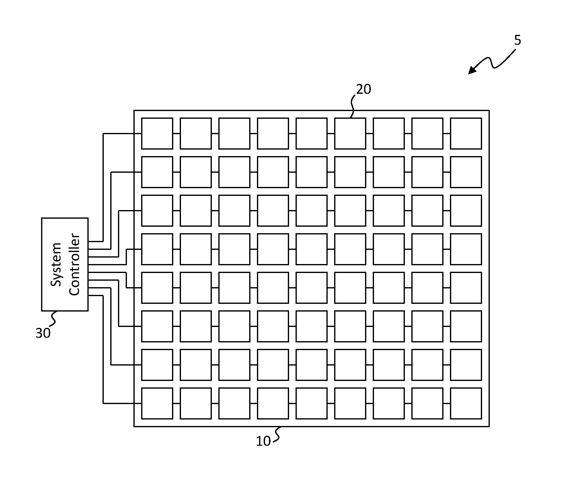
Referring to the schematic of FIG. 1, in an embodiment of the present invention an active-matrix touchscreen 5 includes a substrate 10 and a system controller 30. The system controller 30 can be located on the substrate 10 or externally to it (as shown) and can, for example, be an integrated circuit. The system controller 30 can be a touch system controller or part of a display system controller, for example also controlling pixels in a display. A plurality of spatially separated independent touch elements 20 are disposed on or over the substrate 10, for example in a two-dimensional arrangement. Referring also to FIG. 2, each touch element 20 includes a touch sensor 50 and a touch controller circuit 40 that provides one or more sensor-control signals 42 to the touch sensor 50 and receives one or more sensor-control signals 42 from the touch sensor 50, for example a sense signal 42B responsive to a drive signal 42A. Each touch sensor 50 operates independently of any other touch sensor 50 and can be electrically independent of any other touch sensor 50. Likewise, in an embodiment, each touch controller circuit 40 can operate independently of any other touch controller circuit 40.
In an embodiment and referring back to FIG. 1, the touch elements 20 are connected, for example at least to one neighboring touch element 20 in either or both a row direction or a column direction. The touch elements 20 can be connected in a daisy chain (as shown) or in a row and column matrix (not shown). The touch elements 20 can communicate with each other or through each other and can communicate with the system controller 30, for example using touch transmission circuit 70 in each touch element 20. Thus, a touch element 20 can include touch transmission circuits 70 for receiving a communication from a first touch element 20 and communicating the communication to a second, different touch element 20.
The touch elements 20 can be interconnected in a variety of ways, for example in groups such as rows (as shown in FIG. 1), columns, rows and columns, or in rectangular subsets. The groups of touch elements 20 can be connected to the system controller 30 (for example in rows as shown in FIG. 1), or directly to the system controller 30. In an embodiment, each touch element 20 can independently and simultaneously detect a touch and transmit a touch signal to the system controller 30 in response to the detected touch.
In contrast to the present invention, prior-art touch controllers for a single-sensor touch area (for example resistive or acoustic touch sensors) typically can only detect a single touch at a time and thus do not have a plurality of independent touch elements 20 that can simultaneously detect a touch. Prior-art touch controllers for a multi-sensor touch area (for example self-capacitive or mutual-capacitive touch sensors) activate a row of touch sensors at a time and then read a sense signal from each of the columns. Because rows of sensors are activated together, they are not independent, even though each column provides a separate touch signal in response to the common row activation signal (for example such as a drive signal). Furthermore, according to prior-art schemes, since only one row can be activated at a time, the touch sensors in different rows cannot be activated at the same time and therefore the touch elements in different rows cannot detect a touch at the same time. Moreover, rows are typically sequentially activated so as to detect touches over an entire touch sensor array. This sequential row activation limits the response time of the entire array and hence the size or sensed touch rate of the touch screen. (As will be appreciated by those knowledgeable in the art, rows and columns can be interchanged in the present description and the present invention is not limited by the use of row or column descriptors.)
Thus, according to embodiments of the present invention, a two-dimensional arrangement of touch elements 20 has touch sensors 50 that operate independently of any other touch sensor 50 and touch controller circuits 40 that operate independently of any other touch controller circuit 40. The touch elements 20 can simultaneously detect multiple touches at different location on the substrate 10. To independently and simultaneously detect a touch means that every one of the touch elements 20 in the two-dimensional arrangement can independently detect a touch at the same time. Each of the touch elements 20 can activate a touch sensor 50 with the touch controller circuit 40 and can sense a touch sensor 50 response with the touch controller circuit 40 independently of any other touch element 20, at the same time, or at different times. The separate touch elements 20 can operate at different times, produce different results, and use separate control signals. In one embodiment, the touch controller circuit 40 of only one of the touch elements 20 activates a touch sensor 50 or senses a touch sensor 50 response at a time. In another embodiment, the touch controller circuits 40 of some but not all of the touch elements 20 activates a touch sensor 50 or senses a touch sensor response at a time. The some but not all of the touch elements 20 can include a random selection, complete rows, complete columns, partial rows, partial columns, or rectangular subsets that include only partial rows or partial columns or complete rows or complete columns of the two-dimensional arrangement of touch elements 20. In yet another embodiment, the touch controller circuits 40 of all of the touch elements 20 activate a touch sensor 50 or senses a touch sensor 50 response at a time. Furthermore, the touch controller circuits 40 of independent touch elements 20 can activate or sense touch sensors 50 independently of the system controller, 30 for example without requiring a control, activation, drive, or sense signal from the system controller 30.
In a further embodiment of the present invention, the touch elements 20 respond to an interrogation signal from the system controller 30 with a touch signal communicated by the touch transmission circuit 70. The interrogation signal can be supplied to a single touch element 20 or to multiple touch elements 20. The system controller 30, as shown in FIG. 1, can connect to multiple touch elements 20. The interrogation signal can be supplied to row(s), column(s), or rectangular subsets of touch elements 20. The interrogation signal can be sequentially supplied to subsets of touch elements 20 and groups of touch elements 20 can respond at the same time. Alternatively, the touch elements 20 can independently respond to the interrogation signal, for example with one response at a time. In another embodiment, the touch elements 20 can independently transmit a touch signal to the system controller 30 independently of any other touch element 20 and without responding to an interrogation signal, for example whenever a touch is detected by a respective touch element 20.
In a further embodiment of the present invention, the sensor-control signals 42 include a touch sensor drive signal 42A and a touch sensor sense signal 42B.
Furthermore, each touch element 20 can include a touch analysis circuit 60 that analyzes the sense signal 42B to determine a touch. The touch controller, touch analysis, and touch transmission circuits 40, 60, 70 can include means to drive a sensor at a desired rate, can measure a sensor signal (for example an electrical sense signal from the touch sensor 50), store a measured value in a memory, and can include means to compare a measured value with a stored value (for example with a comparator), as well as including digital circuits for enabling, clearing, or serially communicating signals or stored values. Such circuitry is known in the digital and analog circuit arts and can be integrated into an integrated circuit. Thus, the circuits in the touch elements 20, for example the touch controller circuit 40, the touch analysis circuit 60, and the touch transmission circuit 70 can be made in an integrated circuit. In some embodiments, the touch sensor 50 is made in an integrated circuit, in others it is formed on the substrate 10, or on another substrate.
The touch elements 20 can be dispersed or located on or over the substrate 10 or on or over layers formed on the substrate 10 and can be located in a regular or an irregular arrangement, for example a two-dimensional regular array (as shown in FIG. 1) or in an irregular arrangement (not shown). The plurality of spatially separated independent touch elements 20 can include 10,000 or more independent touch elements 20, 50,000 or more independent touch elements 20, 100,000 or more independent touch elements 20, 500,000 or more independent touch elements 20, or 1,000,000 or more independent touch elements 20. Because the present invention includes touch elements 20 that independently and simultaneously detect a touch, unlike prior-art touch systems, there is no logical limitation on the number of touch elements 20 that can be incorporated onto the substrate 10.
In various embodiments of the present invention, the touch sensor 50 is a capacitive touch sensor, an optical touch sensor, an acoustic touch sensor, an inductive touch sensor, a piezo-electric sensor, or a resistive touch sensor. In an embodiment, the touch sensor 50 is a capacitive touch sensor 50 and includes one or more capacitors, each of which is connected to the touch controller circuit 40. In one embodiment of the present invention, the touch sensor 50 is a self-capacitive touch sensor. In another embodiment, the touch sensor 50 is a mutual-capacitive touch sensor having at least two electrical conductors that can be interdigitated as shown in FIG. 2 with first and second electrical conductors 52, 54 both electrically connected to a common touch controller circuit 40 of the plurality of touch controller circuits 40 with drive and sense signals 42A, 42B. In an alternative arrangement, shown in FIG. 3, the two electrical conductors include a first electrical conductor 52B electrically connected to a first touch controller circuit 40B in a touch element 20B having touch sensor 50B and a second electrical conductor 54B different from the first electrical conductor 52B electrically connected to a second touch controller circuit 40C different from the first touch controller circuit 40B in a touch element 20C having a different touch sensor 50C. Similarly, in touch element 20A, touch controller circuit 40A is connected to first electrical conductor 52A in touch sensor 40A and second electrical conductor 54A is connected to touch controller circuit 40B in touch element 20B. Thus, the first touch controller circuit 40B is connected to a first touch sensor 50B and to a second touch sensor 50A different from the first touch sensor 50B. In this embodiment, the first and second touch sensors 50B, 50A are arranged on opposite sides of the first touch controller circuit 40B.
Referring next to FIG. 4 in an alternative embodiment, the touch sensor 50 is an optical touch sensor 50 that includes a light-sensitive semiconductor diode 80 sensitive to light 82. In such an embodiment, a touch is detected by noting changes in the ambient light level resulting from obscuring light incident on the light-sensitive semiconductor diode 80.
The present invention can be constructed in a variety of ways. In a first way, the touch elements 20 are formed in or on the substrate 10 using photolithographic methods. In a second way, the substrate 10 is a backplane substrate 10 and the touch elements 20 are disposed on one or more touch substrates 14 separate and distinct from the backplane substrate 10. In such an embodiment, for example, the backplane substrate 10 can be glass, plastic, or metal and the touch substrate 14 can be a semiconductor substrate in which the touch controller circuit 40, the touch analysis circuit 60, and the touch transmission circuit 70 are formed and electrically interconnected for example using integrated circuit technologies and materials. The touch substrate 14 can be a crystalline semiconductor substrate having a much higher circuit performance than thin-film semiconductor layers formed on a glass, plastic or metal backplane substrate 10. In a third way, any of the touch controller circuit 40, the touch analysis circuit 60, and the touch transmission circuit 70 are formed in separate semiconductor substrates that are then individually located and interconnected on the backplane substrate 10, for example with photolithographically deposited and patterned metal traces. In a fourth way, each of the touch controller circuit 40, the touch analysis circuit 60, and the touch transmission circuit 70 are formed in two or more semiconductor substrates that are then individually located and interconnected on a separate touch substrate 14, for example made of the same material as the backplane substrate 10. The touch substrate 14 is then mounted and interconnected on the backplane substrate 10. Printed circuit board methods and materials (for example soldering) are useful in mounting and interconnecting multiple substrates on a backplane substrate 10. In any of these embodiments, the substrate 10 can consist of or include one or more of a polymer, plastic, resin, polyimide, PEN, PET, metal, metal foil, glass, a semiconductor, or sapphire. The substrate 10 can have a transparency greater than or equal to 50%, 80%, 90%, or 95% for visible light. The substrate 10 can have a thickness from 5 to 10 microns, 10 to 50 microns, 50 to 100 microns, 100 to 200 microns, 200 to 500 microns, 500 microns to 0.5 mm, 0.5 to 1 mm, 1 mm to 5 mm, 5 mm to 10 mm, or 10 mm to 20 mm and the active-matrix touchscreen 5 can have a thickness from 5 to 10 microns, 10 to 50 microns, 50 to 100 microns, 100 to 200 microns, 200 to 500 microns, 500 microns to 0.5 mm, 0.5 to 1 mm, 1 mm to 5 mm, 5 mm to 10 mm, or 10 mm to 20 mm.
In any of these ways, the touch sensor 50 can be formed on the backplane substrate 10 and connected to the touch controller circuit 40, whether the touch controller circuit 40 is formed in or on the backplane substrate 10 or on a separate touch substrate 14. For example, in an active-matrix touchscreen 5 having touch sensors 50 using capacitors, the capacitors can be constructed on the substrate 10 and have a size that is larger than the various control, analysis, and communication circuits. Alternatively, the touch sensor 50 is formed on a touch substrate 14 separate and distinct from the backplane substrate 10 and located and interconnected on the backplane substrate 10. The touch sensor 50 touch substrate 14 can be independent of any or all of the touch controller circuit 40, the touch analysis circuit 60, and the touch transmission circuit 70 or can be on a common substrate with any one, any combination of, or all of the touch controller circuit 40, the touch analysis circuit 60, and the touch transmission circuit 70. The use of a separate touch substrate 14 and any semiconductor substrates to form any of the touch controller circuit 40, the touch analysis circuit 60, or the touch transmission circuit 70 enhances performance and reduces circuit size because the semiconductor substrates can have a higher performance and denser circuitry than is available in thin-film semiconductor layers such as amorphous silicon layers or low-temperature polysilicon layers formed on, for example, glass substrates or photolithographic methods available for large substrates. The various elements and substrates can be provided using photolithographic methods and located on the backplane substrate 10 using, for example, micro-transfer printing or compound micro-transfer printing.
In yet another embodiment shown in FIG. 5, the active-matrix touch screen includes one or more light emitters 94, for example a red light emitter 94R emitting red light, a green light emitter 94G emitting green light, and a blue light emitter 94B emitting blue light to form a full-color pixel 90. In an embodiment, the light emitters 94 are micro-LEDs and can have at least one of a length, width, or height from 2 to 5 .mu.m, 4 to 10 .mu.m, 10 to 20 .mu.m, or 20 to 50 .mu.m. A pixel controller 92 can control the light emitters 94 under the control of a display controller (not shown). As with the touch elements 20, the light emitters 94 or pixel controller 92 can be formed on the substrate 10 or provided in separate pixel substrates 16 (FIG. 6C) separate and distinct from the backplane substrate 10 and mounted on the backplane substrate 10. The light emitters 94 can each be formed in separate LED substrates that are each also separate and distinct from the pixel substrates 16, touch substrates 14, or backplane substrate 10 and mounted on or disposed on the pixel substrates 16 or backplane substrate 10. The pixel controller 92, and red, green, and blue light emitters 94R, 94G, 94B can each be provided in a separate pixel substrate 16 or in common with each other in various arrangements. Moreover, any of the pixel substrates 16 or touch substrates 14 can be common in various combinations. In particular, the pixel controller 92 can share a substrate with any of the touch controller circuit 40, the touch analysis circuit 60, and the touch transmission circuit 70.
In an example embodiment of an active-matrix touchscreen 5 illustrated in FIG. 6A, a system controller 30 is mounted on a display substrate 10. Touch sensors 50 are formed or otherwise disposed on the display substrate 10. Pixel/touch substrates 12 separate and distinct from the display substrate 10 are disposed on the display substrate 10 and electrically interconnected with the touch sensors 50 (and power and ground signals, not shown). Each of a red, green, and blue micro-LED forming a full-color pixel 90 is formed in a separate LED substrate and disposed adjacent to the pixel/touch substrate 12 on the substrate 10 and electrically connected to the pixel/touch substrate 12. Each pixel/touch substrate 12 is interconnected with a neighboring pixel/touch substrate 12 and includes a touch controller circuit 40 and a pixel controller 92 to control the touch sensor 50 and the LEDs. (Touch analysis and touch transmission circuits 60, 70 can be included in the touch/pixel substrate 12 but, for clarity, are not shown). In an alternative embodiment, the touch controller circuit 40 and the pixel controller 92 are formed in or on a separate touch substrate 14 and pixel substrate 16, respectively, as illustrated in FIG. 6B. In yet another embodiment shown in FIG. 6C, the red, green, and blue micro-LEDs are mounted on the pixel substrate 16. Such a display structure can be formed using micro-transfer techniques, for example using a multi-step transfer or assembly process. By employing such a multi-step transfer or assembly process, increased yields are achieved and thus reduced costs for the active-matrix touchscreen 5 of the present invention. A discussion of compound micro-assembly structures and methods is provided in U.S. Patent Application Ser. No. 62/055,472 filed Sep. 25, 2014, entitled Compound Micro-Assembly Strategies and Devices.
The embodiments illustrated in FIGS. 5 and 6A-6C can be used to construct a display by disposing a plurality of the illustrated touch elements 20 and light emitters 94 together with pixel controllers 92 over the substrate 10. The light emitters 94 can be bottom emitters and the substrate 10 transparent to the light emitted by the light emitters 94. Alternatively, the light emitters 94 can be top emitters and the substrate 10 opaque. The light emitters 94 and pixel controllers 92 can be interspersed between the touch elements 20. In one embodiment, the same number of touch elements 20 and full-color pixels 90 are provided; in another embodiment fewer touch elements 20 than full-color pixels 90 are provided.
Thus, in an embodiment of the present invention, a display incorporating an active-matrix touchscreen 5 includes a substrate 10, a system controller 30, and a plurality of spatially separated independent light-emitters disposed on or over the substrate 10, for example arranged in a two-dimensional array. A plurality of spatially separated independent touch elements 20 is also disposed on or over the substrate 10. The touch elements 20 can be interspersed between the light-emitting full-color pixels 90 over the substrate 10. Each touch element 20 includes a touch sensor 50 and a touch controller circuit 40 that provides one or more sensor-control signals 42 such as a drive signal 42A to the touch sensor 50 and receives a sense signal 42B responsive to the sensor-control signals 42 from the touch sensor 50. As described, each touch sensor 50 operates independently of any other touch sensor 50 to provide a multi-touch active-matrix touchscreen-and-display system.
In an embodiment, any of the light emitters 94, a pixel controller 92, or any portion of the touch elements 20 are formed directly on the substrate 10. In a further embodiment, the substrate 10 is a backplane substrate 10 and the light emitters 94 or pixel controller 92 are provided on a pixel substrate 16 separate and distinct from the backplane substrate 10. In another embodiment, portions of the touch element 20 such as the touch controller circuit 40, the touch analysis circuit 60, the transmission circuit 70, or the touch sensor 50 are provided on a touch substrate 14 separate and distinct from the pixel substrate 16 or the backplane substrate 10. In another embodiment, portions of the touch element 20 such as the touch controller circuit 40, the touch analysis circuit 60, the transmission circuit 70, or the touch sensor 50 are provided on the touch substrate 14, the pixel substrate 16 or a combined pixel/touch substrate 12. Additional details useful in understanding and performing aspects of the present invention are described in U.S. patent application Ser. No. 14/754,573 filed Jun. 29, 2015, entitled Small Aperture Ratio Display with Electrical Component and U.S. patent application Ser. No. 14/743,981 filed Jun. 18, 2015 and entitled Micro-Assembled Micro LED Displays and Lighting Elements.
Thus, in an embodiment of the present invention, an integrated display includes a substrate 10, a plurality of light emitters 94 disposed on the substrate 10 and a plurality of touch sensors 50 disposed exclusively on the substrate 10. By exclusively disposed on the substrate 10 is meant that none of the light emitters 94 or touch sensors 50 are located or formed on another substrate that extends over the entire display area (where the display area is the contiguous area of the substrate 10 that includes all of the light emitters 94). LEDs or touch sensors formed on a native substrate different from the display substrate 10 and transferred, for example by micro-transfer printing, onto the non-native display substrate 10 are disposed on the substrate 10.
In certain embodiments, the LEDs are formed on or in a native substrate different from the display substrate 10 and then integrated on an intermediate pixel, touch, or combined pixel/touch substrate 16, 14, 12 and then transferred as part of the intermediate substrate, for example by micro-transfer printing, onto the non-native display substrate 10 are also disposed on the substrate 10. A discussion of compound micro-assembly structures and methods is provided in U.S. Patent Application Ser. No. 62/055,472 filed Sep. 25, 2014, entitled Compound Micro-Assembly Strategies and Devices.
In certain embodiments, touch sensors 50 formed on the substrate 10 are also disposed exclusively on the substrate 10. Thus, in an embodiment, the touch sensors 50 are in or on a common plane with the light emitters 94 so that the touch sensors 50 do not absorb light emitted by the light emitters 94 and are not located between the light emitters 94 and a touchscreen user or display viewer, for example as illustrated in FIGS. 6A-6C. Such an arrangement of touch sensors 50 and light emitters 94 improves the light output of the display by preventing the touchscreen from absorbing light emitted by the light emitters 94.
In a further embodiment of the present invention, one or more of the touch sensors 50 are interspersed between the light emitters 94 over the substrate 10 in the display area. Furthermore, an array of touch controller circuits 40 can be disposed over the substrate 10. Each touch controller circuit 40 is associated with, connected to, and controls one or more of the touch sensors 40.
In operation, external power and ground signals (not shown) are provided to the array of touch elements 20. Each touch controller circuit 40 repeatedly and independently provides drive signals 42A to a corresponding touch sensor 50 and receives or detects sense signals 42B in response that indicate a touch or no-touch. The sensor-control signals 42 are analyzed, for example using the touch analysis circuit 60. Such a circuit can store sensed signals either as an analog value or as a digitized value, and then compare the stored sense signals to sense signals obtained at a later moment in time to detect changes in the touch sensor 50 sensor signals 42B indicative of a touch, for example changes in an electrical sense signal representing capacitance or ambient light. If a meaningful change is noted, the touch transmission circuit 70 communicates the touch to the system controller 30.
Thus, in an embodiment of the present invention and referring to FIG. 9, a method of operating an active-matrix touchscreen 5 includes providing power and ground signals to an array of spatially separated independent touch elements disposed over a substrate in step 100. In certain embodiments, each touch element includes a touch sensor and a touch controller circuit. As discussed above, each touch sensor can operate independently of any other touch sensor of the array of touch elements. In step 110, each of the touch controller circuits 40 independently provides one or more sensor-control signals to the touch sensors 50. Thereafter, in step 120 each of the touch controller circuits 40 independently receives a sense signal responsive to the one or more sensor-control signals from the touch sensor 50. The sense signal, or a determined touch signal, is transmitted to the system controller 30 in step 150.
In optional step 130, the touch elements analyze sense signals to determine whether a touch has taken place and, if a touch is determined to have taken place, a touch signal is generated and transmitted to the system controller 30 in step 150. In optional step 140, an interrogation signal is received from the system controller 30 and, if a touch has taken place, the touch signal is transmitted to the system controller 30 in step 150.
In one embodiment, the system controller 30 interrogates each of the touch elements 20 in turn, for example by interconnecting them with a row-column matrix electrode structure. Referring to FIG. 7, if the touch transmission circuit 70 of a touch element 20 receives a high signal from both a row and a column electrode and a touch is present at the touch element 20, a touch signal is returned. If any of the three signals are not present, no touch signal is returned. The system controller 30 receives the touch signal, or not, and then interrogates another touch element 20. The interrogation of each touch element 20 is completely independent of any other touch element 20 and the touch elements 20 can be interrogated in any order or frequency, for example touch elements 20 in the center of the two-dimensional array of touch elements 20 can be interrogated more frequently than other touch elements 20 on the periphery of the two-dimensional array of touch elements 20. The touch signal at the touch element 20 can be left valid until the touch is removed so that the touch element 20 can be repeatedly interrogated and transmits a touch signal. Alternatively, the combination of the row and column electrode interrogation signals (the AND combination of the row and column signals) can be used to clear the touch signal at the touch element 20. Alternatively, the system controller 30 can use any interrogation signal desired, including a direct connection to each individual touch element 20 or multiple groups of matrix-addressed subsets of touch elements 20, obviating the need for row and column matrix-addressed interrogation signals. The system controller 30 can include multiple circuits or connections to enable multiple touch elements 20 to report simultaneously, for example by subsets such as rows or columns.
Referring to FIG. 8, in another embodiment the system controller 30 does not interrogate the touch elements 20 but rather receives and responds to touch signals independently provided by the touch elements 20. For example, the touch controller circuit 40 of each touch element 20 independently and separately drives each touch sensor 50 with the drive signal 42A and receives a sense signal 42B that is analyzed by the touch analysis circuit 60. When a touch is detected the touch transmission circuit 70 of each independent touch element 20 receives a touch signal that is stored in a latch, for example using a local store signal (e.g., derived from a locally generated clock or a clock that is broadcast to all of the touch elements 20 in the array of touch elements 20) and a local enable signal brought high to indicate that a touch is present. A control signal from the system controller 30 indicates whether another touch element 20 is communicating (for example using an OR function of the row and column touch signals). If another touch element 20 is communicating, the output AND gate is not enabled and the touch transmission circuit 70 does not indicate a touch on the row and column address lines. If another touch element 20 is not communicating, the control line is low and the touch output enabled if a touch is present and stored in the latch. The system controller 30 will receive the row and column signals that indicate the address of the touch in the array and raise the control flag. When the row and column signals are properly stored in the system controller 30, the control signal is brought low again and in response a local clear signal is brought high to clear the latch and reset the local touch element 20 system.
Although the FIG. 8 circuit provides an address with a row and column signal, other schemes are possible. For example a direct connection can be provided to the system controller 30, obviating the need for the control signal. Alternatively, multiple control signals could be unique to a subset of touch elements 20 (for example a row or column) enabling a touch element 20 in each subset to report at the same instant. The system controller 30 can include multiple circuits or connections to enable multiple touch elements 20 to report simultaneously, for example by subsets such as rows or columns.
In another embodiment, referring back to FIG. 1, the touch elements 20 are connected in rows of daisy-chained touch elements 20. Each chain of touch elements 20 can simultaneously and serially communicate down the respective row and the touch transmission circuits 70 in each touch element 20 receives and transmits signals from its neighbors in the row, eventually passing the information to the system controller 30. Thus, the system controller 30 can receive touch information from every row at the same time. Chains can include single rows or columns or multiple rows or columns, increasing the data rate (or reducing response time) and reducing the connections required. Digital logic circuits suitable for the embodiments of FIGS. 7 and 8 or for daisy-chained control and communications as shown in FIG. 1 can be made in integrated circuits using photolithographic methods known in the art. Small integrated circuits can be micro transfer printed to the substrate 10 to provide the desired functionality disposed over the substrate 10. For example, the spatially separated independent touch elements 20 can be disposed on the substrate 10 via micro transfer printing. Known methods of patterning substrates 10 with electrical conductors (for example using micro-wires) are available.
Because the touch elements 20 of the present invention include active elements such as transistors, storage, or control elements, an active-matrix touchscreen 5 of the present invention is not limited to a data rate limited by sequential scanning rates, since all of the touch elements are operating simultaneously and independently. This attribute of present invention enables larger touchscreens or touchscreens with greater resolution, or both. In an embodiment of the present invention, the plurality of touch elements 20 have a resolution of greater than or equal to 10 touch sensors per inch, greater than or equal to 20 touch sensors per inch, greater than or equal to 50 touch sensors per inch, greater than or equal to 75 touch sensors per inch, greater than or equal to 100 touch sensors per inch, greater than or equal to 200 touch sensors per inch, or greater than or equal to 400 touch sensors per inch and least one dimension of the touch sensors 50 over the substrate 10 is less than or equal to 0.1 inches, 0.08 inches, 0.06 inches, 0.05 inches, 0.033 inches, 0.025, 0.020, 0.015, or 0.01 inches. Alternatively, at least two orthogonal dimensions of the touch sensors are both less than or equal to 0.1 inches, 0.08 inches, 0.06 inches, 0.05 inches, 0.033 inches, 0.025, 0.020, 0.015, or 0.01 inches. Likewise, at least one dimension of the substrate area over which the touch sensors 50 are disposed is greater than or equal to 10 inches, 12 inches, 15 inches, 20 inches, 24 inches, 32 inches, 44 inches, 55 inches, 65 inches, 72 inches, 80 inches, 100 inches, or 110 inches.
In a further embodiment of the present invention, the touch elements 20 include storage elements that provide double-buffered circuitry to communicate a touch to the system controller 30 and simultaneously sense a second touch at the same time with the touch controller circuit 40 and the touch sensor 50. Thus, the touch elements 20 are continuously available to both sense touches and communicate touches.
The circuit diagrams provided in FIGS. 6 and 7 are illustrative. Other circuit designs accomplishing the same tasks are readily apparent to skilled circuit designers and can include more sophisticated communication and control functions.
As is understood by those skilled in the art, the terms "over", "under", "above", "below", "beneath", and "on" are relative terms and can be interchanged in reference to different orientations of the layers, elements, and substrates included in the present invention. For example, a first layer on a second layer, in some embodiments means a first layer directly on and in contact with a second layer. In other embodiments, a first layer on a second layer can include another layer there between.
Having described certain embodiments, it will now become apparent to one of skill in the art that other embodiments incorporating the concepts of the disclosure may be used. Therefore, the invention should not be limited to the described embodiments, but rather should be limited only by the spirit and scope of the following claims.
Throughout the description, where apparatus and systems are described as having, including, or comprising specific components, or where processes and methods are described as having, including, or comprising specific steps, it is contemplated that, additionally, there are apparatus, and systems of the disclosed technology that consist essentially of, or consist of, the recited components, and that there are processes and methods according to the disclosed technology that consist essentially of, or consist of, the recited processing steps.
It should be understood that the order of steps or order for performing certain action is immaterial so long as the disclosed technology remains operable. Moreover, two or more steps or actions in some circumstances can be conducted simultaneously. The invention has been described in detail with particular reference to certain embodiments thereof, but it will be understood that variations and modifications can be effected within the spirit and scope of the invention.
PARTS LIST
5 active-matrix touchscreen 10 substrate/display substrate/backplane substrate 12 pixel/touch substrate 14 touch substrate 16 pixel substrate 20, 20A, 20B, 20C touch element 30 system controller 40, 40A, 40B, 40C touch controller circuit 42 sensor-control signals 42A drive signal 42B sense signal 50, 50A, 50B, 50C touch sensor 52, 52A, 52B, 52C first electrical conductor 54, 54A, 54B, 54C second electrical conductor 60 touch analysis circuit 70 touch transmission circuit 80 light-sensitive semiconductor diode 82 light 90 full-color pixel 92 pixel controller 94 light emitters 94R red light emitter 94G green light emitter 94B blue light emitter 100 provide power and ground signals to substrate and touch elements step 110 touch controller circuits send sensor-control signals to touch sensors step 120 touch controller circuits receive sense signals from touch sensors step 130 touch elements analyze sense signals to determine touch step 140 touch elements receive interrogation signal from system controller step 150 touch elements transmit touch so system controller step
* * * * *
D00000
D00001
D00002
D00003
D00004
D00005
D00006
D00007
D00008
D00009
D00010
XML
uspto.report is an independent third-party trademark research tool that is not affiliated, endorsed, or sponsored by the United States Patent and Trademark Office (USPTO) or any other governmental organization. The information provided by uspto.report is based on publicly available data at the time of writing and is intended for informational purposes only.
While we strive to provide accurate and up-to-date information, we do not guarantee the accuracy, completeness, reliability, or suitability of the information displayed on this site. The use of this site is at your own risk. Any reliance you place on such information is therefore strictly at your own risk.
All official trademark data, including owner information, should be verified by visiting the official USPTO website at www.uspto.gov. This site is not intended to replace professional legal advice and should not be used as a substitute for consulting with a legal professional who is knowledgeable about trademark law.