Light-emitting Device And An Electronic Apparatus Including The Same
PARK; Myoungjin ; et al.
U.S. patent application number 17/508480 was filed with the patent office on 2022-04-28 for light-emitting device and an electronic apparatus including the same. The applicant listed for this patent is Samsung Display Co., Ltd. Invention is credited to Jingoo Kang, Changhee Lee, Jaeyong Lee, Jaehong Park, Myoungjin PARK, Seokgyu Yoon.
| Application Number | 20220131108 17/508480 |
| Document ID | / |
| Family ID | |
| Filed Date | 2022-04-28 |


View All Diagrams
| United States Patent Application | 20220131108 |
| Kind Code | A1 |
| PARK; Myoungjin ; et al. | April 28, 2022 |
LIGHT-EMITTING DEVICE AND AN ELECTRONIC APPARATUS INCLUDING THE SAME
Abstract
A light-emitting device includes: a first electrode; a second electrode; an interlayer between the first electrode and the second electrode and including an emission layer; a hole transport region between the first electrode and the emission layer; and an electron transport region between the second electrode and the emission layer, wherein the first electrode is a multi-layered electrode including: a first layer including a first material, a second layer disposed on the first layer and including a second material, and a third layer between the second layer and the hole transport region and including a third material, wherein a first surface of the third layer contacts the second layer, and a second surface of the third layer facing the first surface directly contacts the hole transport region, and the third material has a work function of greater than about 4.8 eV and less than or equal to about 6.8 eV.
| Inventors: | PARK; Myoungjin; (Yongin-si, KR) ; Lee; Changhee; (Yongin-si, KR) ; Park; Jaehong; (Yongin-si, KR) ; Kang; Jingoo; (Yongin-si, KR) ; Yoon; Seokgyu; (Yongin-si, KR) ; Lee; Jaeyong; (Yongin-si, KR) | ||||||||||
| Applicant: |
|
||||||||||
|---|---|---|---|---|---|---|---|---|---|---|---|
| Appl. No.: | 17/508480 | ||||||||||
| Filed: | October 22, 2021 |
| International Class: | H01L 51/52 20060101 H01L051/52; H01L 51/50 20060101 H01L051/50 |
Foreign Application Data
| Date | Code | Application Number |
|---|---|---|
| Oct 23, 2020 | KR | 10-2020-0138585 |
Claims
1. A light-emitting device comprising: a first electrode; a second electrode; an interlayer between the first electrode and the second electrode and comprising an emission layer; a hole transport region between the first electrode and the emission layer; and an electron transport region between the second electrode and the emission layer, wherein the first electrode is a multi-layered electrode comprising: a first layer comprising a first material, a second layer disposed on the first layer and comprising a second material, and a third layer between the second layer and the hole transport region and comprising a third material, wherein a first surface of the third layer contacts the second layer, and a second surface of the third layer facing the first surface directly contacts the hole transport region, and the third material has a work function of greater than about 4.8 eV and less than or equal to about 6.8 eV.
2. The light-emitting device of claim 1, wherein the hole transport region comprises an organic compound, an inorganic compound, or a combination thereof, the electron transport region comprises an inorganic compound, and the emission layer comprises quantum dots.
3. The light-emitting device of claim 1, wherein the hole transport region comprises a hole injection layer, a hole transport layer, an emission auxiliary layer, an electron blocking layer, or any combination thereof, the electron transport region comprises a hole blocking layer, an electron transport layer, an electron injection layer, or any combination thereof, and the second surface of the third layer directly contacts any one of the hole injection layer and the hole transport layer.
4. The light-emitting device of claim 3, wherein the second surface of the third layer and the hole injection layer directly contact each other to form a continuous interface between the third layer and the hole injection layer.
5. The light-emitting device of claim 1, wherein the hole transport region does not comprise a crystalline carbon layer.
6. The light-emitting device of claim 1, wherein the first material comprises a transparent conductive material.
7. The light-emitting device of claim 6, wherein the transparent conductive material comprises an indium tin oxide, an indium zinc oxide, a tin oxide, a zinc oxide, or any combination thereof.
8. The light-emitting device of claim 1, wherein the second material comprises a reflective conductive material.
9. The light-emitting device of claim 8, wherein the second material comprises silver, aluminum, an aluminum alloy, or any combination thereof.
10. The light-emitting device of claim 1, wherein the third material comprises a semi-transparent conductive material.
11. The light-emitting device of claim 10, wherein the semi-transparent conductive material comprises one or more oxides of at least one metal of W, Ni, V, Cr, Ti, Mo, Cu, Ta, or Co.
12. The light-emitting device of claim 1, wherein the first material comprises an indium tin oxide, the second material comprises Ag, Al, an Al alloy, or a combination thereof, and the third material comprises WO.sub.3, NiO, V.sub.2O.sub.5, CrO.sub.3-x wherein x defined by 0.ltoreq.x.ltoreq.1, TiO.sub.2, MoO.sub.3, MoO.sub.2, CuO, Ta.sub.2O.sub.5, Co.sub.3O.sub.4, or a combination thereof.
13. The light-emitting device of claim 1, wherein the emission layer comprises a quantum dot having a core-shell structure including a core and a shell, the core including a first semiconductor material, and the shell including a second semiconductor material.
14. The light-emitting device of claim 13, wherein the first semiconductor material and the second semiconductor material each, independently from one another, comprise a Group 12-Group 16-based compound, a Group 13-Group 15-based compound, a Group 14-Group 16-based compound, a Group 11-Group 13-Group 16-based compound, a Group 11-Group 12-Group 13-Group 16-based compound, or any combination thereof.
15. The light-emitting device of claim 13, wherein the first semiconductor material and the second semiconductor material each, independently from one another, comprise InP, InN, InSb, InAs, InAsP, InGaAs, InGaP, ZnS, ZnSe, ZnSeS, ZnTe, ZnTeSe, GaP, GaN, GaSb, GaAs, CuInS, CuInZnS, AgInS.sub.2, CdSe, CdS, CdTe, HgSe, HgTe, CdZnSe, CdSeTe, ZnCdSe, In.sub.2S.sub.3, Ga.sub.2S.sub.3, PbS, PbSe, PbTe, or any combination thereof.
16. The light-emitting device of claim 13, wherein the first semiconductor material comprises InP, InN, InSb, InAs, InAsP, InGaAs, InGaP, ZnS, ZnSe, ZnSeS, ZnTe, ZnTeSe, GaP, GaN, GaSb, GaAs, CuInS, CuInZnS, AgInS.sub.2, CdSe, CdS, CdTe, HgSe, HgTe, CdZnSe, CdSeTe, ZnCdSe, or any combination thereof, and the second semiconductor material comprises ZnSe, ZnS, In.sub.2S.sub.3, Ga.sub.2S.sub.3, or any combination thereof.
17. The light-emitting device of claim 1, wherein the electron transport region comprises an electron transport layer, and the electron transport layer comprises ZnO, TiO.sub.2, WO.sub.3, SnO.sub.2, Mg-doped ZnO, Al-doped ZnO, Ga-doped ZnO, In-doped ZnO, ZnSiO.sub.x wherein x defined by 0<x<5, Al-doped TiO.sub.2, Ga-doped TiO.sub.2, In-doped TiO.sub.2, Al-doped WO.sub.3, Ga-doped WO.sub.3, In-doped WO.sub.3, Al-doped SnO.sub.2, Ga-doped SnO.sub.2, In-doped SnO.sub.2, or any combination thereof.
18. The light-emitting device of claim 1, wherein the light-emitting device comprises a top-emission light-emitting device to pass outgoing light through the second electrode, wherein the outgoing light comprises a first reflected light emitted from the emission layer and reflected by the third layer, second reflected light passed through the third layer and reflected by the second layer, and amplified light formed by constructive interference between the first reflected light and the second reflected light.
19. An electronic apparatus comprising the light-emitting device of claim 1.
20. A flat panel display apparatus comprising: a thin-film transistor including a source electrode, a drain electrode, and an activation layer; and the light-emitting device of claim 1, wherein the first electrode of the light-emitting device is electrically connected with one of the source electrode and the drain electrode of the thin-film transistor.
Description
CROSS-REFERENCE TO RELATED APPLICATION
[0001] This application claims priority from and the benefit of Korean Patent Application No. 10-2020-0138585, filed on Oct. 23, 2020, which is hereby incorporated by reference for all purposes as if fully set forth herein.
BACKGROUND
[0002] Embodiments of the invention relate generally to light-emitting devices and, more particularly, to light-emitting devices having a multi-layered electrode.
DISCUSSION OF THE BACKGROUND
[0003] A light-emitting device includes an anode, a cathode, and an emission layer formed therebetween. Holes injected from the anode combine with electrons injected from the cathode in the emission layer to form excitons, which transition from an excited state to a ground state, thereby generating light.
[0004] Light-emitting devices may be driven at a low voltage and formed as a light-weight thin film, and may have excellent characteristics in terms of viewing angles, contrast, and response speed. Accordingly, they may be used in a personal portable device such as an MP3 player or a mobile phone to a television (TV).
[0005] The above information disclosed in this Background section is only for understanding of the background of the inventive concepts, and, therefore, it may contain information that does not constitute prior art.
SUMMARY
[0006] Light-emitting devices constructed according to the principles and illustrative implementations of the invention are capable of increasing resonance efficiency by using an electrode, such as an anode, having a novel structure and a low driving voltage obtained according to a decrease in the thickness of a hole transport region. For example, when a multi-layered electrode including a third layer is disposed between a second layer and a hole transport region and includes a third material having a work function of greater than about 4.8 eV and less than or equal to about 6.8 eV, an increase in light efficiency due to constructive interference of a light emission wavelength according to the generation of secondary resonance and a decrease in driving voltage according to the thickness of a hole transport region may be obtained, thereby resulting in a low driving voltage and high efficiency.
[0007] Additional features of the inventive concepts will be set forth in the description which follows, and in part will be apparent from the description, or may be learned by practice of the inventive concepts.
[0008] According to one aspect of the invention, a light-emitting device includes: a first electrode; a second electrode; an interlayer between the first electrode and the second electrode and including an emission layer; a hole transport region between the first electrode and the emission layer; and an electron transport region between the second electrode and the emission layer, wherein the first electrode is a multi-layered electrode including: a first layer including a first material, a second layer disposed on the first layer and including a second material, and a third layer between the second layer and the hole transport region and including a third material, wherein a first surface of the third layer contacts the second layer, and a second surface of the third layer facing the first surface directly contacts the hole transport region, and the third material has a work function of greater than about 4.8 eV and less than or equal to about 6.8 eV.
[0009] The hole transport region may include an organic compound, an inorganic compound, or a combination thereof, the electron transport region may include an inorganic compound, and the emission layer may include quantum dots.
[0010] The hole transport region may include a hole injection layer, a hole transport layer, an emission auxiliary layer, an electron blocking layer, or any combination thereof, the electron transport region may include a hole blocking layer, an electron transport layer, an electron injection layer, or any combination thereof, and the second surface of the third layer may directly contact at least one of the hole injection layer and the hole transport layer.
[0011] The second surface of the third layer and the hole injection layer may directly contact each other to form a continuous interface between the third layer and the hole injection layer.
[0012] The hole transport region may not include a crystalline carbon layer.
[0013] The first material may include a transparent conductive material.
[0014] The transparent conductive material may include an indium tin oxide, an indium zinc oxide, a tin oxide, a zinc oxide, or any combination thereof.
[0015] The second material may include a reflective conductive material.
[0016] The second material may include silver, aluminum, an aluminum alloy, or a combination thereof.
[0017] The third material may include a semi-transparent conductive material.
[0018] The semi-transparent conductive material may include one or more oxides of at least one metal of W, Ni, V, Cr, Ti, Mo, Cu, Ta, or Co.
[0019] The first material may include an indium tin oxide, the second material may include Ag, Al, an Al alloy, or a combination thereof, and the third material may include WO.sub.3, NiO, V.sub.2O.sub.5, CrO.sub.3-x wherein x defined by 0.ltoreq.x.ltoreq.1, TiO.sub.2, MoO.sub.3, MoO.sub.2, CuO, Ta.sub.2O.sub.5, Co.sub.3O.sub.4, or a combination thereof.
[0020] The emission layer may include a quantum dot having a core-shell structure including a core and a shell, the core including a first semiconductor material, and the shell including a second semiconductor material.
[0021] The first semiconductor material and the second semiconductor material each, independently from one another, may include a Group 12-Group 16-based compound, a Group 13-Group 15-based compound, a Group 14-Group 16-based compound, a Group 11-Group 13-Group 16-based compound, a Group 11-Group 12-Group 13-Group 16-based compound, or any combination thereof.
[0022] The first semiconductor material and the second semiconductor material each, independently from one another, may include InP, InN, InSb, InAs, InAsP, InGaAs, InGaP, ZnS, ZnSe, ZnSeS, ZnTe, ZnTeSe, GaP, GaN, GaSb, GaAs, CuInS, CuInZnS, AgInS.sub.2, CdSe, CdS, CdTe, HgSe, HgTe, CdZnSe, CdSeTe, ZnCdSe, In.sub.2S.sub.3, Ga.sub.2S.sub.3, PbS, PbSe, PbTe, or any combination thereof.
[0023] The first semiconductor material may include InP, InN, InSb, InAs, InAsP, InGaAs, InGaP, ZnS, ZnSe, ZnSeS, ZnTe, ZnTeSe, GaP, GaN, GaSb, GaAs, CuInS, CuInZnS, AgInS.sub.2, CdSe, CdS, CdTe, HgSe, HgTe, CdZnSe, CdSeTe, ZnCdSe, or any combination thereof, and the second semiconductor material may include ZnSe, ZnS, In.sub.2S.sub.3, Ga.sub.2S.sub.3, or any combination thereof.
[0024] The electron transport region may include an electron transport layer, and the electron transport layer may include ZnO, TiO.sub.2, WO.sub.3, SnO.sub.2, Mg-doped ZnO, Al-doped ZnO, Ga-doped ZnO, In-doped ZnO, ZnSiO.sub.x wherein x defined by 0<x<5, Al-doped TiO.sub.2, Ga-doped TiO.sub.2, In-doped TiO.sub.2, Al-doped WO.sub.3, Ga-doped WO.sub.3, In-doped WO.sub.3, Al-doped SnO.sub.2, Ga-doped SnO.sub.2, In-doped SnO.sub.2, or any combination thereof.
[0025] The light-emitting device may include a top-emission light-emitting device to pass outgoing light through the second electrode, wherein the outgoing light may include a first reflected light emitted from the emission layer and reflected by the third layer, second reflected light passed through the third layer and reflected by the second layer, and amplified light formed by constructive interference between the first reflected light and the second reflected light.
[0026] An electronic apparatus may include the light-emitting device as described above.
[0027] A flat panel display apparatus may include: a thin-film transistor including a source electrode, a drain electrode, and an activation layer; and the light-emitting device, as described above, wherein the first electrode of the light-emitting device may be electrically connected with one of the source electrode and the drain electrode of the thin-film transistor.
[0028] According to another aspect of the invention, a light-emitting device includes: a first electrode; a second electrode; an interlayer between the first electrode and the second electrode and including an emission layer; a hole transport region between the first electrode and the emission layer; and an electron transport region between the second electrode and the emission layer, wherein the first electrode is a multi-layered electrode including a first layer including a first material, a second layer disposed on the first layer and including a second material, and a third layer between the second layer and the hole transport region and including a third material, wherein a first surface of the third layer contacts the second layer, and a second surface of the third layer facing the first surface directly contacts the hole transport region, and the third material has a work function of greater than about 4.8 eV and less than or equal to about 6.8 eV.
[0029] The hole transport region may include an organic compound, an inorganic compound, or a combination thereof, the electron transport region may include an inorganic compound, and the emission layer may include quantum dots.
[0030] The hole transport region may include a hole injection layer, a hole transport layer, an emission auxiliary layer, an electron blocking layer, or any combination thereof, the electron transport region may include a hole blocking layer, an electron transport layer, an electron injection layer, or any combination thereof, and the second surface of the third layer may directly contact any one of the hole injection layer and the hole transport layer.
[0031] The second surface of the third layer and the hole injection layer may directly contact each other to form a continuous interface between the third layer and the hole injection layer.
[0032] The hole transport region may not include a crystalline carbon layer.
[0033] The first material may include a transparent conductive material.
[0034] The transparent conductive material may include an indium tin oxide, an indium zinc oxide, a tin oxide, a zinc oxide, or any combination thereof.
[0035] The second material may include a reflective conductive material.
[0036] The second material may include silver, aluminum, an aluminum alloy, or a combination thereof.
[0037] The third material may include a semi-transparent conductive material.
[0038] The semi-transparent conductive material may include one or more oxides of at least one metal of W, Ni, V, Cr, Ti, Mo, Cu, Ta, or Co.
[0039] The first material may include an indium tin oxide, the second material may include Ag, Al, an Al alloy, or a combination thereof, and the third material may include WO.sub.3, NiO, V.sub.2O.sub.5, CrO.sub.3-x wherein x defined by 0.ltoreq.x.ltoreq..sub.1, TiO.sub.2, MoO.sub.3, MoO.sub.2, CuO, Ta.sub.2O.sub.5, Co.sub.3O.sub.4, or a combination thereof.
[0040] The emission layer may include a quantum dot having a core-shell structure including a core and a shell, the core including a first semiconductor material, and the shell including a second semiconductor material.
[0041] The first semiconductor material and the second semiconductor material each, independently from one another, may include a compound having one or more elements of Groups 12-16, a compound having one or more elements of Groups 13-15, a compound having one or more elements of Groups 14-16, a compound having one or more elements of Group 11, and Groups 13-16, a Group 11-12-13-16 compound, or a combination thereof.
[0042] The first semiconductor material and the second semiconductor material each, independently from one another, may include InP, InN, InSb, InAs, InAsP, InGaAs, InGaP, ZnS, ZnSe, ZnSeS, ZnTe, ZnTeSe, GaP, GaN, GaSb, GaAs, CuInS, CuInZnS, AgInS.sub.2, CdSe, CdS, CdTe, HgSe, HgTe, CdZnSe, CdSeTe, ZnCdSe, In.sub.2S.sub.3, Ga.sub.2S.sub.3, PbS, PbSe, PbTe, or any combination thereof.
[0043] The first semiconductor material may include InP, InN, InSb, InAs, InAsP, InGaAs, InGaP, ZnS, ZnSe, ZnSeS, ZnTe, ZnTeSe, GaP, GaN, GaSb, GaAs, CuInS, CuInZnS, AgInS.sub.2, CdSe, CdS, CdTe, HgSe, HgTe, CdZnSe, CdSeTe, ZnCdSe, or any combination thereof, and the second semiconductor material may include ZnSe, ZnS, In.sub.2S.sub.3, Ga.sub.2S.sub.3, or any combination thereof.
[0044] The electron transport region may include an electron transport layer, and the electron transport layer may include ZnO, TiO.sub.2, WO.sub.3, SnO.sub.2, Mg-doped ZnO, Al-doped ZnO, Ga-doped ZnO, In-doped ZnO, ZnSiO.sub.x wherein x defined by 0<x<5, Al-doped TiO.sub.2, Ga-doped TiO.sub.2, In-doped TiO.sub.2, Al-doped WO.sub.3, Ga-doped WO.sub.3, In-doped WO.sub.3, Al-doped SnO.sub.2, Ga-doped SnO.sub.2, In-doped SnO.sub.2, or any combination thereof.
[0045] The light-emitting device may include a top-emission light-emitting device to pass outgoing light through the second electrode, wherein the outgoing light may include a first reflected light emitted from the emission layer and reflected by the third layer, second reflected light passed through the third layer and reflected by the second layer, and amplified light formed by constructive interference between the first reflected light and the second reflected light.
[0046] An electronic apparatus may include the light-emitting device as described above.
[0047] A flat panel display apparatus may include: a thin-film transistor including a source electrode, a drain electrode, and an activation layer; and the light-emitting device, as described above, wherein the first electrode of the light-emitting device may be electrically connected with one of the source electrode and the drain electrode of the thin-film transistor.
[0048] It is to be understood that both the foregoing general description and the following detailed description are exemplary and explanatory and are intended to provide further explanation of the invention as claimed.
BRIEF DESCRIPTION OF THE DRAWINGS
[0049] The accompanying drawings, which are included to provide a further understanding of the invention and are incorporated in and constitute a part of this specification, illustrate exemplary embodiments of the invention, and together with the description serve to explain the inventive concepts.
[0050] FIG. 1 is a schematic view of an embodiment of a light-emitting device constructed according to the principles of the invention.
[0051] FIG. 2 is a schematic view of another embodiment of a light-emitting device constructed according to the principles of the invention.
[0052] FIG. 3 is a cross-sectional view of an embodiment of a light-emitting device constructed according to the principles of the invention.
[0053] FIG. 4 is a cross-sectional view of another embodiment of a light-emitting device constructed according to the principles of the invention.
[0054] FIG. 5 is a diagram depicting the correlation between the thickness of a hole transport region and a third layer of an embodiment of a light-emitting device constructed according to the principles of the invention.
[0055] FIG. 6A is a graph depicting the refractive index of each of ITO and WO.sub.3 layers with respect to wavelength in a comparative example and an embodiment of the invention.
[0056] FIG. 6B is a graph depicting the light absorption coefficient of each of ITO and WO.sub.3 layers with respect to wavelength in a comparative example and an embodiment of the invention.
[0057] FIG. 7 is a graph depicting a change in luminance according to thickness of a hole injection layer of a blue light-emitting device including a multi-layered electrode constructed according to an embodiment of the invention.
[0058] FIG. 8 is a graph depicting a change in luminance according to thickness of a hole injection layer of a green light-emitting device including a multi-layered electrode constructed according to an embodiment of the invention.
[0059] FIG. 9 is a graph showing a change in luminance according to thickness of a hole injection layer of a red light-emitting device including a multi-layered electrode constructed according to an embodiment of the invention.
DETAILED DESCRIPTION
[0060] In the following description, for the purposes of explanation, numerous specific details are set forth in order to provide a thorough understanding of various exemplary embodiments or implementations of the invention. As used herein "embodiments" and "implementations" are interchangeable words that are non-limiting examples of devices or methods employing one or more of the inventive concepts disclosed herein. It is apparent, however, that various exemplary embodiments may be practiced without these specific details or with one or more equivalent arrangements. In other instances, well-known structures and devices are shown in block diagram form in order to avoid unnecessarily obscuring various exemplary embodiments. Further, various exemplary embodiments may be different, but do not have to be exclusive. For example, specific shapes, configurations, and characteristics of an exemplary embodiment may be used or implemented in another exemplary embodiment without departing from the inventive concepts.
[0061] Unless otherwise specified, the illustrated exemplary embodiments are to be understood as providing exemplary features of varying detail of some ways in which the inventive concepts may be implemented in practice. Therefore, unless otherwise specified, the features, components, modules, layers, films, panels, regions, plates, and/or aspects, etc. (hereinafter individually or collectively referred to as "elements"), of the various embodiments may be otherwise combined, separated, interchanged, and/or rearranged without departing from the inventive concepts.
[0062] The use of cross-hatching and/or shading in the accompanying drawings is generally provided to clarify boundaries between adjacent elements. As such, neither the presence nor the absence of cross-hatching or shading conveys or indicates any preference or requirement for particular materials, material properties, dimensions, proportions, commonalities between illustrated elements, and/or any other characteristic, attribute, property, etc., of the elements, unless specified. Further, in the accompanying drawings, the size and relative sizes of elements may be exaggerated for clarity and/or descriptive purposes. When an exemplary embodiment may be implemented differently, a specific process order may be performed differently from the described order. For example, two consecutively described processes may be performed substantially at the same time or performed in an order opposite to the described order. Also, like reference numerals denote like elements.
[0063] When an element, such as a layer, is referred to as being "on," "connected to," or "coupled to" another element or layer, it may be directly on, connected to, or coupled to the other element or layer or intervening elements or layers may be present. When, however, an element or layer is referred to as being "directly on," "directly connected to," or "directly coupled to" another element or layer, there are no intervening elements or layers present. To this end, the term "connected" may refer to physical, electrical, and/or fluid connection, with or without intervening elements. Further, the D1-axis, the D2-axis, and the D3-axis are not limited to three axes of a rectangular coordinate system, such as the x, y, and z-axes, and may be interpreted in a broader sense. For example, the D1-axis, the D2-axis, and the D3-axis may be perpendicular to one another, or may represent different directions that are not perpendicular to one another. For the purposes of this disclosure, "at least one of X, Y, and Z" and "at least one selected from the group consisting of X, Y, and Z" may be construed as X only, Y only, Z only, or any combination of two or more of X, Y, and Z, such as, for instance, XYZ, XYY, YZ, and ZZ. As used herein, the term "and/or" includes any and all combinations of one or more of the associated listed items.
[0064] Although the terms "first," "second," etc. may be used herein to describe various types of elements, these elements should not be limited by these terms. These terms are used to distinguish one element from another element. Thus, a first element discussed below could be termed a second element without departing from the teachings of the disclosure.
[0065] Spatially relative terms, such as "beneath," "below," "under," "lower," "above," "upper," "over," "higher," "side" (e.g., as in "sidewall"), and the like, may be used herein for descriptive purposes, and, thereby, to describe one elements relationship to another element(s) as illustrated in the drawings. Spatially relative terms are intended to encompass different orientations of an apparatus in use, operation, and/or manufacture in addition to the orientation depicted in the drawings. For example, if the apparatus in the drawings is turned over, elements described as "below" or "beneath" other elements or features would then be oriented "above" the other elements or features. Thus, the exemplary term "below" can encompass both an orientation of above and below. Furthermore, the apparatus may be otherwise oriented (e.g., rotated 90 degrees or at other orientations), and, as such, the spatially relative descriptors used herein interpreted accordingly.
[0066] The terminology used herein is for the purpose of describing particular embodiments and is not intended to be limiting. As used herein, the singular forms, "a," "an," and "the" are intended to include the plural forms as well, unless the context clearly indicates otherwise. Moreover, the terms "comprises," "comprising," "includes," and/or "including," when used in this specification, specify the presence of stated features, integers, steps, operations, elements, components, and/or groups thereof, but do not preclude the presence or addition of one or more other features, integers, steps, operations, elements, components, and/or groups thereof. It is also noted that, as used herein, the terms "substantially," "about," and other similar terms, are used as terms of approximation and not as terms of degree, and, as such, are utilized to account for inherent deviations in measured, calculated, and/or provided values that would be recognized by one of ordinary skill in the art.
[0067] Various exemplary embodiments are described herein with reference to sectional and/or exploded illustrations that are schematic illustrations of idealized exemplary embodiments and/or intermediate structures. As such, variations from the shapes of the illustrations as a result, for example, of manufacturing techniques and/or tolerances, are to be expected. Thus, exemplary embodiments disclosed herein should not necessarily be construed as limited to the particular illustrated shapes of regions, but are to include deviations in shapes that result from, for instance, manufacturing. In this manner, regions illustrated in the drawings may be schematic in nature and the shapes of these regions may not reflect actual shapes of regions of a device and, as such, are not necessarily intended to be limiting.
[0068] Unless otherwise defined, all terms (including technical and scientific terms) used herein have the same meaning as commonly understood by one of ordinary skill in the art to which this disclosure is a part. Terms, such as those defined in commonly used dictionaries, should be interpreted as having a meaning that is consistent with their meaning in the context of the relevant art and should not be interpreted in an idealized or overly formal sense, unless expressly so defined herein.
Description of FIG. 1
[0069] FIG. 1 is a schematic view of an embodiment of a light-emitting device constructed according to the principles of the invention.
[0070] Hereinafter, the structure of the light-emitting device 10 according to an embodiment and a method of manufacturing the light-emitting device 10 will be described in connection with FIG. 1.
[0071] Referring to FIG. 1, the light-emitting device 10 includes: a first electrode 110; a second electrode 150 facing the first electrode 110; an interlayer 130 located between the first electrode 110 and the second electrode 150 and including an emission layer 131; a hole transport region 120 located between the first electrode 110 and the emission layer 131; and an electron transport region 140 located between the second electrode 150 and the emission layer 131; and the first electrode 110 is a multi-layered electrode including a first layer 111 including a first material, a second layer 112 located on the first layer 111 and including a second material, and a third layer 113 located between the second layer 112 and the hole transport region 120 and including a third material, and a first surface S1 of the third layer 113 may be in contact with the second layer 112 and a second surface S2 of the third layer 113 facing the first surface S1 thereof may be in direct contact with the hole transport region 120, and the third material may have a work function of greater than about 4.8 eV and less than or equal to about 6.8 eV.
[0072] The light-emitting device 10 is a top emission type light-emitting device 10, and the outgoing light passing through the second electrode 150 may include first reflected light that is emitted from the emission layer 131 and is reflected by the third layer 113, second reflected light that passes through the third layer 113 and is reflected by the second layer 112, and amplified light that is formed by constructive interference between the first reflected light and the second reflected light.
[0073] For constructive interference of outgoing light from the first electrode 110, the light-emitting device 10 may be modified with respect to the thicknesses of the first electrode 110 and the hole transport region 120, for example, the thicknesses of the third layer 113 and the hole transport region 120.
[0074] After repeated experiments, the inventors discovered a significant and unexpected correlation of the thicknesses of the third layer 113 and the hole transport region 120. Namely, they discovered that these thicknesses cause constructive interference by making the wavelength of the outgoing light having passed through the third layer 113 and reflected by the second layer 112 to have substantially the same phase as the wavelength of outgoing light reflected from the third layer 113. Due to the formation of the third layer 113 with a third material whose work function is greater than about 4.8 eV and less than or equal to about 6.8 eV, Equation 1 is derived.
Y = - A X + B Equation .times. .times. 1 ##EQU00001##
[0075] FIG. 5 is a diagram depicting the correlation between the thickness of a hole transport region and a third layer of an embodiment of a light-emitting device constructed according to the principles of the invention.
[0076] In this regard, Y is the thickness of the hole transport region (hole injection layer and hole transport layer); X is the thickness of the third layer; A is a natural number from 1 to 1.3; B is the correction value according to the emission wavelength. In this regard, the correlation between the third layer and hole transport region thickness is shown as a graph in FIG. 5.
[0077] Hereinafter, the structure of the light-emitting device 10 according to an embodiment and a method of manufacturing the light-emitting device 10 will be described in connection with FIG. 1.
First Electrode 110
[0078] In FIG. 1, a substrate may be additionally located under the first electrode 110 or above the second electrode 150. As the substrate, a glass substrate or a plastic substrate may be used. In an embodiment, the substrate may be a flexible substrate, and may include plastics with excellent heat resistance and durability, such as a polyimide, a polyethylene terephthalate (PET), a polycarbonate, a polyethylene naphthalate, a polyarylate (PAR), a polyetherimide, or any combination thereof.
[0079] The first electrode 110 may be formed by, for example, depositing or sputtering a material for forming the first electrode 110 on the substrate. When the first electrode 110 is an anode, a material for forming the first electrode 110 may be a high work function material that facilitates injection of holes. The first electrode 110 may include the first layer 111, the second layer 112, and the third layer 113.
[0080] The first layer 111 may be provided on the substrate, and, to be formed as a transparent electrode, an indium tin oxide (ITO), an indium zinc oxide (IZO), a tin oxide (SnO.sub.2), zinc oxide (ZnO), or any combination thereof, may be used as the first material.
[0081] The second layer 112 may be provided on the first layer, and, to be formed as a reflective electrode, silver (Ag), aluminum (Al), an aluminum alloy (an Al alloy), or any combination thereof may be used as the second material.
[0082] The third layer 113 may be provided on the second layer, and, to be formed as a semi-transparent electrode, at least one oxide of metal selected from W, Ni, V, Cr, Ti, Mo, Cu, Ta and Co may be used as the third material. The first layer, the second layer, and the third layer may include different materials. In an embodiment, the first layer and the third layer may include different materials.
[0083] In an embodiment, the first material may include the ITO, the second material may include Ag, Al, an Al alloy, or a combination thereof, and the third material may include WO.sub.3, NiO, V.sub.2O.sub.5, CrO.sub.3-x (wherein x is defined by 0.ltoreq.x.ltoreq.1), TiO.sub.2, MoO.sub.3, MoO.sub.2, CuO, Ta.sub.2O.sub.5, Co.sub.3O.sub.4, or a combination thereof.
[0084] The ITO has a work function value of 4.8 electron volt (eV), and the work functions of these third materials are measured using ultraviolet photoelectron spectroscopy (UPS) measuring equipment, and all of them exceed 4.8 eV as shown in Table 1 below.
TABLE-US-00001 TABLE 1 Work Material function (eV) TiO.sub.2 5.4 MoO.sub.3 6.8 MoO.sub.2 5.9 CuO 5.9 Ta.sub.2O.sub.5 5.2 NiO 6.3 WO.sub.3 6.8 V.sub.2O.sub.5 6.8 CrO.sub.3-x, (0 .ltoreq. x .ltoreq. 1) 6.8 Co.sub.3O.sub.4 6.3
[0085] In the first electrode having a composite multi-layer structure manufactured using different materials, some of incident light from the emission layer may reach the second layer through the third layer, and the light reaching the second layer may be reflected by the reflective electrode and emitted to the outside, and the remaining light may be reflected by the third layer and emitted to the outside. In this case, as the thickness of the third layer is adjusted, phases of wavelengths of the reflected lights coincide with each other, and thus, optical amplification is generated by constructive interference, and as a result, luminance and efficiency may be increased.
Interlayer 130
[0086] The interlayer 130 may be located on the first electrode 110. The interlayer 130 may include an emission layer 131. The interlayer 130 may further include a hole transport region 120 located between the first electrode 110 and the emission layer 131, and an electron transport region 140 located between the emission layer 131 and the second electrode 150.
[0087] The interlayer 130 may further include metal element-containing compounds such as organometallic compounds, inorganic materials such as quantum dots, and the like, in addition to various organic materials.
[0088] In one or more embodiments, the interlayer 130 may include, i) two or more emitting units sequentially stacked between the first electrode 110 and the second electrode 150 and ii) a charge generation layer located between the two emitting units. When the interlayer 130 includes the emitting unit and the charge generation layer as described above, the light-emitting device 10 may be a tandem light-emitting device.
Hole Transport Region in Interlayer 130
[0089] The hole transport region may have: i) a single-layered structure consisting of a single layer consisting of a single material, ii) a single-layered structure consisting of a single layer consisting of a plurality of different materials, or iii) a multi-layered structure including a plurality of layers including different materials. The hole transport region may include a hole injection layer, a hole transport layer, an emission auxiliary layer, an electron blocking layer, or any combination thereof.
[0090] For example, the hole transport region may have a multi-layered structure including a hole injection layer/hole transport layer structure, a hole injection layer/hole transport layer/emission auxiliary layer structure, a hole injection layer/emission auxiliary layer structure, a hole transport layer/emission auxiliary layer structure, or a hole injection layer/hole transport layer/electron blocking layer structure, wherein, in each structure, layers are stacked sequentially from the first electrode 110.
[0091] The hole transport region 120 may be arranged such that the second surface S2 of the third layer 113 of the first electrode 110 directly contacts the hole injection layer. Thus, the hole transport region 120 may have a continuous interface between the third layer and the hole injection layer. The hole transport region 120 may not include a crystalline carbon layer. In an embodiment, the crystalline carbon layer includes one or more of carbon nanoplates, carbon nanotubes, and the like.
[0092] The hole transport region 120 may include a compound represented by Formula 201, a compound represented by Formula 202, or any combination thereof:
##STR00001##
[0093] wherein, in Formulae 201 and 202,
[0094] L.sub.201 to L.sub.204 may each independently be a C.sub.3-C.sub.60 carbocyclic group unsubstituted or substituted with at least one R.sub.10a or a C.sub.1-C.sub.60 heterocyclic group unsubstituted or substituted with at least one R10a,
[0095] L.sub.205 may be *--O--*', *--S--*', *--N(Q.sub.201)-*', a C.sub.1-C.sub.20 alkylene group unsubstituted or substituted with at least one R.sub.10a, a C.sub.2-C.sub.20 alkenylene group unsubstituted or substituted with at least one R.sub.10a, a C.sub.3-C.sub.60 carbocyclic group unsubstituted or substituted with at least one R.sub.10a, or a C.sub.1-C.sub.60 heterocyclic group unsubstituted or substituted with at least one R.sub.10a,
[0096] xa1 to xa4 may each independently an integer from 0 to 5,
[0097] xa5 may be an integer from 1 to 10,
[0098] R.sub.201 to R.sub.204 and Q.sub.201 may each independently be a C.sub.3-C.sub.60 carbocyclic group unsubstituted or substituted with at least one R.sub.10a or a C.sub.1-C.sub.60 heterocyclic group unsubstituted or substituted with at least one R.sub.10a,
[0099] R.sub.201 and R.sub.202 may optionally be linked to each other, via a single bond, to form a C.sub.1-C.sub.5 alkylene group unsubstituted or substituted with at least one R.sub.10a, or a C.sub.2-C.sub.5 alkenylene group unsubstituted or substituted with at least one R.sub.10a, to form a C.sub.8-C.sub.60 polycyclic group (for example, a carbazole group or the like) unsubstituted or substituted with at least one R.sub.10a (see Compound HT16 or the like),
[0100] R.sub.203 and R.sub.204 may optionally be linked to each other, via a single bond, a C.sub.1-C.sub.5 alkylene group unsubstituted or substituted with at least one R.sub.10a, or a C.sub.2-C.sub.5 alkenylene group unsubstituted or substituted with at least one R.sub.10a, to form a C.sub.8-C.sub.60 polycyclic group unsubstituted or substituted with at least one R.sub.10a, and
[0101] na1 is an integer from 1 to 4.
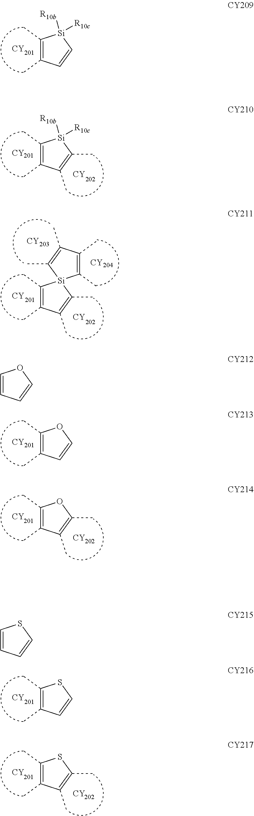
[0102] In one or more embodiments, each of Formulae 201 and 202 may include at least one of groups represented by Formulae CY201 to CY217.
##STR00002## ##STR00003##
[0103] The variables R.sub.10b and R.sub.10c in Formulae CY201 to CY217 are the same as described in connection with R.sub.10a, and ring CY.sub.201 to ring CY.sub.204 may each independently be a C.sub.3-C.sub.20 carbocyclic group or a C.sub.1-C.sub.20 heterocyclic group, and at least one hydrogen in Formulae CY201 to CY217 may be unsubstituted or substituted with at least one R.sub.10a.
[0104] In an embodiment, ring CY.sub.201 to ring CY.sub.204 in Formulae CY201 to CY217 may each independently be a benzene group, a naphthalene group, a phenanthrene group, or an anthracene group. In one or more embodiments, each of Formulae 201 and 202 may include at least one of groups represented by Formulae CY201 to CY203. In one or more embodiments, Formula 201 may include at least one of groups represented by Formulae CY201 to CY203 and at least one of groups represented by Formulae CY204 to CY217.
[0105] In one or more embodiments, xa1 in Formula 201 is 1, R.sub.201 is a group represented by one of Formulae CY201 to CY203, xa2 may be 0, and R.sub.202 may be a group represented by one of Formulae CY204 to CY207. In one or more embodiments, each of Formulae 201 and 202 may not include a group represented by one of Formulae CY201 to CY203.
[0106] In one or more embodiments, each of Formulae 201 and 202 may not include a group represented by one of Formulae CY201 to CY203, and may include at least one of groups represented by Formulae CY204 to CY217. In an embodiment, each of Formulae 201 and 202 may not include a group represented by one of Formulae CY201 to CY217.
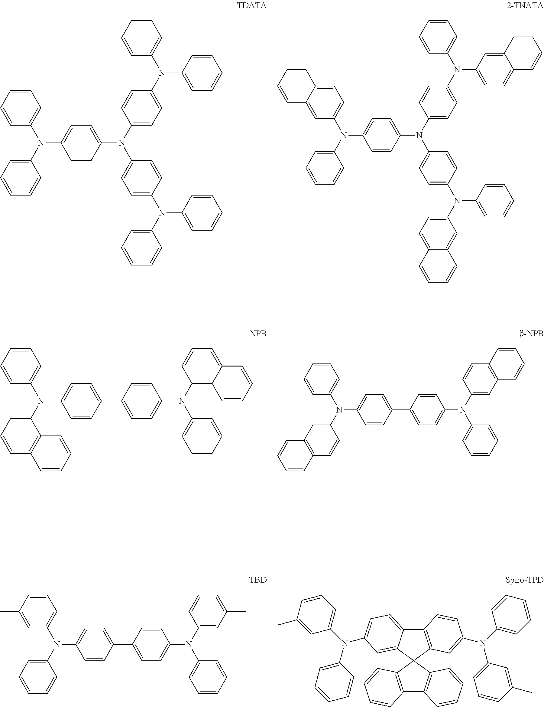
[0107] In an embodiment, the hole transport region may include one of Compounds HT1 to HT44, 4,4',4''-tris[phenyl(m-tolyl)amino]triphenylamine (m-MTDATA), 1-N,1-N-bis[4-(diphenylamino)phenyl]-4-N,4-N-diphenylbenzene-1,4-diamine (TDATA), 4,4', 4''-tris[2-naphthyl(phenyl)amino]triphenylamine (2-TNATA), N,N'-di(1-naphthyl)-N,N'-diphenyl-(1,1'-biphenyl)-4,4'-diamine (NPB or NPD), N4,N4'-di(naphthalen-2-yl)-N4,N4'-diphenyl-[1,1'-biphenyl]-4,4'-dia- mine (.beta.-NPB), N,N'-bis(3-methylphenyl)-N,N'-diphenylbenzidine (TPD), N,N'-bis(3-methylphenyl)-N,N'-diphenyl-9,9-spirobifluorene-2,7-diamine (Spiro-TPD), N2,N7-di(1-naphthalenyl)-N2,N7-diphenyl-9,9'-spirobi[9H-fluorene]-2,7-dia- mine (Spiro-NPB), N, N,N'-di(1-naphthyl)-N,N'-2,2'-dimethyldiphenyl-(1,1'-biphenyl)-4,4'-diami- ne (methylated-NPB), 4,4'-cyclohexylidenebis[N,N-bis(4-methylphenyl)benzenamine] (TAPC), N,N,N',N'-tetrakis(3-methylphenyl)-3,3'-dimethylbenzidine (HMTPD), 4,4', 4''-tris(N-carbazolyl)triphenylamine (TCTA), polyaniline/dodecylbenzenesulfonic acid (PANI/DBSA), poly(3,4-ethylenedioxythiophene)/poly(4-styrenesulfonate) (PEDOT/PSS), polyaniline/camphor sulfonic acid (PANI/CSA), polyaniline/poly(4-styrenesulfonate) (PANI/PSS), or any combination thereof:
##STR00004## ##STR00005## ##STR00006## ##STR00007## ##STR00008## ##STR00009## ##STR00010## ##STR00011## ##STR00012## ##STR00013##
[0108] The thickness of the hole transport region may be in a range of about 50 .ANG. to about 10,000 .ANG., for example, about 100 .ANG. to about 4,000 .ANG.. When the hole transport region includes a hole injection layer, a hole transport layer, or any combination thereof, the thickness of the hole injection layer may be in a range of about 100 .ANG. to about 9,000 .ANG., for example, about 100 .ANG. to about 1,000 .ANG., and the thickness of the hole transport layer may be in a range of about 50 .ANG. to about 2,000 .ANG., for example, about 100 .ANG. to about 1,500 .ANG.. When the thicknesses of the hole transport region, the hole injection layer and the hole transport layer are within these ranges, satisfactory hole transporting characteristics may be obtained without a substantial increase in driving voltage.
[0109] The emission auxiliary layer may increase light-emission efficiency by compensating for an optical resonance distance according to the wavelength of light emitted by an emission layer, and the electron-blocking layer may block the flow of electrons from an electron transport region. The emission auxiliary layer and the electron-blocking layer may include the materials as described above.
P-Dopant
[0110] The hole transport region may further include, in addition to these materials, a charge-generation material for the improvement of conductive properties. The charge-generation material may be uniformly or non-uniformly dispersed in the hole transport region (for example, in the form of a single layer consisting of a charge-generation material).
[0111] The charge-generation material may be, for example, a p-dopant. In one embodiment, the lowest unoccupied molecular orbital (LUMO) energy level of the p-dopant may be about -3.5 eV or less.
[0112] In an embodiment, the p-dopant may include a quinone derivative, a cyano group-containing compound, a compound containing element EL1 and element EL2, or any combination thereof. Examples of the quinone derivative are tetracyanoquinodimethane (TCNQ), 2,3,5,6-tetrafluoro-7,7,8,8-tetracyanoquinodimethane (F4-TCNQ), etc.
[0113] Examples of the cyano group-containing compound are 1,4,5,8,9,12-hexaazatriphenylene-hexacarbonitrile (HAT-CN), and a compound represented by Formula 221 below.
##STR00014##
[0114] In Formula 221,
[0115] R.sub.221 to R.sub.223 may each independently be a C.sub.3-C.sub.60 carbocyclic group unsubstituted or substituted with at least one R.sub.10a or a C.sub.1-C.sub.60 heterocyclic group unsubstituted or substituted with at least one R.sub.10a, and
[0116] at least one of R.sub.221 to R.sub.223 may each independently be a C.sub.3-C.sub.60 carbocyclic group or a C.sub.1-C.sub.60 heterocyclic group, each substituted with a cyano group; --F; --Cl; --Br; --I; a C.sub.1-C.sub.20 alkyl group substituted with a cyano group, --F, --Cl, --Br, --I, or any combination thereof; or any combination thereof.
[0117] In the compound containing element EL1 and element EL2, element EL1 may be metal, metalloid, or a combination thereof, and element EL2 may be non-metal, metalloid, or a combination thereof.
[0118] Examples of the metal are an alkali metal (for example, lithium (Li), sodium (Na), potassium (K), rubidium (Rb), cesium (Cs), etc.); alkaline earth metal (for example, beryllium (Be), magnesium (Mg), calcium (Ca), strontium (Sr), barium (Ba), etc.); transition metal (for example, titanium (Ti), zirconium (Zr), hafnium (Hf), vanadium (V), niobium (Nb), tantalum (Ta), chromium (Cr), molybdenum (Mo), tungsten (W), manganese (Mn), technetium (Tc), rhenium (Re), iron (Fe), ruthenium (Ru), osmium (Os), cobalt (Co), rhodium (Rh), iridium (Ir), nickel (Ni), palladium (Pd), platinum (Pt), copper (Cu), silver (Ag), gold (Au), etc.); post-transition metal (for example, zinc (Zn), indium (In), tin (Sn), etc.); and lanthanide metal (for example, lanthanum (La), cerium (Ce), praseodymium (Pr), neodymium (Nd), promethium (Pm), samarium (Sm), europium (Eu), gadolinium (Gd), terbium (Tb), dysprosium (Dy), holmium (Ho), erbium (Er), thulium (Tm), ytterbium (Yb), lutetium (Lu), etc.).
[0119] Examples of the metalloid are silicon (Si), antimony (Sb), and tellurium (Te). Examples of the non-metal are oxygen (O) and halogen (for example, F, Cl, Br, I, etc.).
[0120] In an embodiment, examples of the compound containing element EL1 and element EL2 are metal oxide, metal halide (for example, metal fluoride, metal chloride, metal bromide, or metal iodide), metalloid halide (for example, metalloid fluoride, metalloid chloride, metalloid bromide, or metalloid iodide), metal telluride, or any combination thereof.
[0121] Examples of the metal oxide are tungsten oxide (for example, WO, W.sub.2O.sub.3, WO.sub.2, WO.sub.3, W.sub.2O.sub.5, etc.), vanadium oxide (for example, VO, V.sub.2O.sub.3, VO.sub.2, V.sub.2O.sub.5, etc.), molybdenum oxide (MoO, Mo.sub.2O.sub.3, MoO.sub.2, MoO.sub.3, Mo.sub.2O.sub.5, etc.), and rhenium oxide (for example, ReO.sub.3, etc.).
[0122] Examples of the metal halide are alkali metal halide, alkaline earth metal halide, transition metal halide, post-transition metal halide, and lanthanide metal halide. Examples of the alkali metal halide are LiF, NaF, KF, RbF, CsF, LiCl, NaCl, KCl, RbCl, CsCl, LiBr, NaBr, KBr, RbBr, CsBr, LiI, NaI, KI, RbI, and CsI. Examples of the alkaline earth metal halide are BeF.sub.2, MgF.sub.2, CaF.sub.2, SrF.sub.2, BaF.sub.2, BeCl.sub.2, MgCl.sub.2, CaCl.sub.2, SrCl.sub.2, BaCl.sub.2, BeBr.sub.2, MgBr.sub.2, CaBr.sub.2, SrBr.sub.2, BaBr.sub.2, BeI.sub.2, MgI.sub.2, CaI.sub.2, SrI.sub.2, and BaI.sub.2.
[0123] Examples of the transition metal halide are titanium halide (for example, TiF.sub.4, TiCl.sub.4, TiBr.sub.4, TiI.sub.4, etc.), zirconium halide (for example, ZrF.sub.4, ZrCl.sub.4, ZrBr.sub.4, ZrI.sub.4, etc.), hafnium halide (for example, HfF.sub.4, HfCl.sub.4, HfBr.sub.4, HfI.sub.4, etc.), vanadium halide (for example, VF.sub.3, VCl.sub.3, VBr.sub.3, VI.sub.3, etc.), niobium halide (for example, NbF.sub.3, NbCl.sub.3, NbBr.sub.3, NbI.sub.3, etc.), tantalum halide (for example, TaF.sub.3, TaCl.sub.3, TaBr.sub.3, TaI.sub.3, etc.), chromium halide (for example, CrF.sub.3, CrCl.sub.3, CrBr.sub.3, CrI.sub.3, etc.), molybdenum halide (for example, MoF.sub.3, MoCl.sub.3, MoBr.sub.3, MoI.sub.3, etc.), tungsten halide (for example, WF.sub.3, WCl.sub.3, WBr.sub.3, WI.sub.3, etc.), manganese halide (for example, MnF.sub.2, MnCl.sub.2, MnBr.sub.2, MnI.sub.2, etc.), technetium halide (for example, TcF.sub.2, TcCl.sub.2, TcBr.sub.2, TcI.sub.2, etc.), rhenium halide (for example, ReF.sub.2, ReCl.sub.2, ReBr.sub.2, ReI.sub.2, etc.), iron halide (for example, FeF.sub.2, FeCl.sub.2, FeBr.sub.2, FeI.sub.2, etc.), ruthenium halide (for example, RuF.sub.2, RuCl.sub.2, RuBr.sub.2, RuI.sub.2, etc.), osmium halide (for example, OsF.sub.2, OsCl.sub.2, OsBr.sub.2, OsI.sub.2, etc.), cobalt halide (for example, CoF.sub.2, CoCl.sub.2, CoBr.sub.2, CoI.sub.2, etc.), rhodium halide (for example, RhF.sub.2, RhCl.sub.2, RhBr.sub.2, RhI.sub.2, etc.), iridium halide (for example, IrF.sub.2, IrCl.sub.2, IrBr.sub.2, IrI.sub.2, etc.), nickel halide (for example, NiF.sub.2, NiCl.sub.2, NiBr.sub.2, NiI.sub.2, etc.), palladium halide (for example, PdF.sub.2, PdCl.sub.2, PdBr.sub.2, PdI.sub.2, etc.), platinum halide (for example, PtF.sub.2, PtCl.sub.2, PtBr.sub.2, PtI.sub.2, etc.), copper halide (for example, CuF, CuCl, CuBr, CuI, etc.), silver halide (for example, AgF, AgCl, AgBr, AgI, etc.), and gold halide (for example, AuF, AuCl, AuBr, AuI, etc.).
[0124] Examples of the post-transition metal halide are zinc halide (for example, ZnF.sub.2, ZnCl.sub.2, ZnBr.sub.2, ZnI.sub.2, etc.), indium halide (for example, InI.sub.3, etc.), and tin halide (for example, SnI.sub.2, etc.). Examples of the lanthanide metal halide are YbF, YbF.sub.2, YbF.sub.3, SmF.sub.3, YbCl, YbCl.sub.2, YbCl.sub.3, SmCl.sub.3, YbBr, YbBr.sub.2, YbBr.sub.3, SmBr.sub.3, YbI, YbI.sub.2, YbI.sub.3, and SmI.sub.3. An example of the metalloid halide is antimony halide (for example, SbCls, etc.).
[0125] Examples of the metal telluride are alkali metal telluride (for example, Li.sub.2Te, Na.sub.2Te, K.sub.2Te, Rb.sub.2Te, Cs.sub.2Te, etc.), alkaline earth metal telluride (for example, BeTe, MgTe, CaTe, SrTe, BaTe, etc.), transition metal telluride (for example, TiTe.sub.2, ZrTe.sub.2, HfTe.sub.2, V.sub.2Te.sub.3, Nb.sub.2Te.sub.3, Ta.sub.2Te.sub.3, Cr.sub.2Te.sub.3, Mo.sub.2Te.sub.3, W.sub.2Te.sub.3, MnTe, TcTe, ReTe, FeTe, RuTe, OsTe, CoTe, RhTe, IrTe, NiTe, PdTe, PtTe, Cu.sub.2Te, CuTe, Ag.sub.2Te, AgTe, Au.sub.2Te, etc.), post-transition metal telluride (for example, ZnTe, etc.), and lanthanide metal telluride (for example, LaTe, CeTe, PrTe, NdTe, PmTe, EuTe, GdTe, TbTe, DyTe, HoTe, ErTe, TmTe, YbTe, LuTe, etc.).
Emission Layer 131 in Interlayer 130
[0126] The emission layer 131 may be a single layer or may have a structure in which two or more layers are stacked. In an embodiment, the emission layer 131 may have a single-layered structure or a structure in which two to ten layers are stacked.
[0127] The emission layer 131 may be an inorganic emission layer including at least one selected from quantum dots and perovskite. Quantum dots are a spherical semiconductor nanomaterial having a size of several to several hundreds of nanometer, and may include a core including a material having a small band gap and a shell located to surround the core.
[0128] The quantum dots may have a core-shell structure including a core including a first semiconductor crystal and a shell including a second semiconductor crystal. The first semiconductor and the second semiconductor may each independently include a Group 12-Group 16-based compound, a Group 13-Group 15-based compound, a Group 14-Group 16-based compound, a Group 11-Group 13-Group 16-based compound, a Group 11-Group 12-Group 13-Group 16-based compound, or any combination thereof.
[0129] For example, the first semiconductor and the second semiconductor may each independently include InP, InN, InSb, InAs, InAsP, InGaAs, InGaP, ZnS, ZnSe, ZnSeS, ZnTe, ZnTeSe, GaP, GaN, GaSb, GaAs, CuInS, CuInZnS, AgInS.sub.2, CdSe, CdS, CdTe, HgSe, HgTe, CdZnSe, CdSeTe, ZnCdSe, In.sub.2S.sub.3, Ga.sub.2S.sub.3, PbS, PbSe, PbTe, or any combination thereof.
[0130] In an embodiment, the first semiconductor may include InP, InN, InSb, InAs, InAsP, InGaAs, InGaP, ZnS, ZnSe, ZnSeS, ZnTe, ZnTeSe, GaP, GaN, GaSb, GaAs, CuInS, CuInZnS, AgInS.sub.2, CdSe, CdS, CdTe, HgSe, HgTe, CdZnSe, CdSeTe, ZnCdSe, or any combination thereof, and the second semiconductor may include ZnSe, ZnS, In.sub.2S.sub.3, Ga.sub.2S.sub.3, or any combination thereof.
[0131] In an embodiment, the quantum dots may include more ligands bound to the shell. For example, the ligand may be an oleic acid, an octylamine, a decylamine, a mercaptopropionic acid, a dodecanethiol, an 1-octanethiol, a thionyl chloride, and any combination thereof. Quantum dots are dispersed in a naturally coordinated form in a dispersion medium such as an organic solvent or a polymer resin, and the dispersion medium may be any transparent medium that does not affect the wavelength conversion performance of the quantum dots, does not change by light or reflect light, and does not cause absorption of light. For example, the organic solvent may include at least one of a toluene, a chloroform, and an ethanol, and the polymer resin may include at least one of an epoxy, a silicone, a polystylene, and an acrylate.
[0132] Unlike a bulky material, quantum dots have a discontinuous band gap energy due to the quantum confinement effect. In addition, regarding a quantum dot, a gap between energy bands varies according to the size of the quantum dot, and even when the same quantum dot is used, light with different wavelengths may be emitted when the size thereof is different. The smaller the size of the quantum dot, the greater the band gap energy. Accordingly, light having a shorter wavelength may be emitted. Using these characteristics, the size of the quantum dot is adjusted by appropriately changing the growth condition of the nanocrystal to obtain light of the desired wavelength range. Therefore, by introducing such a quantum dot into a light-emitting device, a light-emitting device having high light efficiency and color purity may be implemented.
Electron Transport Region 140
[0133] The electron transport region may have: i) a single-layered structure consisting of a single layer consisting of a single material, ii) a single-layered structure consisting of a single layer consisting of a plurality of different materials, or iii) a multi-layered structure including a plurality of layers including different materials.
[0134] The electron transport region may include a buffer layer, a hole blocking layer, an electron control layer, an electron transport layer, an electron injection layer, or any combination thereof.
[0135] In an embodiment, the electron transport region may have an electron transport layer/electron injection layer structure, a hole blocking layer/electron transport layer/electron injection layer structure, an electron control layer/electron transport layer/electron injection layer structure, or a buffer layer/electron transport layer/electron injection layer structure, wherein, for each structure, constituting layers are sequentially stacked from an emission layer.
[0136] In an embodiment, the electron transport region (for example, the buffer layer, the hole blocking layer, the electron control layer, or the electron transport layer in the electron transport region) may include a metal-free compound including at least one .pi. electron-deficient nitrogen-containing C.sub.1-C.sub.60 cyclic group.
[0137] In an embodiment, the electron transport region may include a compound represented by Formula 601 below:
[Ar.sub.601].sub.xe11-[(L.sub.601).sub.xe1-R.sub.601].sub.ex21 Formula 601
[0138] wherein, in Formula 601,
[0139] Ar.sub.601 and L.sub.601 may each independently be a C.sub.3-C.sub.60 carbocyclic group unsubstituted or substituted with at least one R.sub.10a or a C.sub.1-C.sub.60 heterocyclic group unsubstituted or substituted with at least one R.sub.10a,
[0140] xe11 may be 1, 2, or 3,
[0141] xe1 may be 0, 1, 2, 3, 4, or 5,
[0142] R.sub.601 may be a C.sub.3-C.sub.60 carbocyclic group unsubstituted or substituted with at least one R.sub.10a, a C.sub.1-C.sub.60 heterocyclic group unsubstituted or substituted with at least one R.sub.10a, --Si(Q.sub.601)(Q.sub.602)(Q.sub.603), --C(.dbd.O)(Q.sub.601), --S(.dbd.O).sub.2(Q.sub.601), or --P(.dbd.O)(Q.sub.601)(Q.sub.602),
[0143] Q.sub.601 to Q.sub.603 are the same as described in connection with Q.sub.11,
[0144] xe21 may be 1, 2, 3, 4, or 5,
[0145] at least one of Ar.sub.601, L.sub.601, and R.sub.601 may each independently be a .pi. electron-deficient nitrogen-containing C.sub.1-C.sub.60 cyclic group unsubstituted or substituted with at least one R.sub.10a.
[0146] For example, when xe11 in Formula 601 is 2 or more, two or more of Ar.sub.601(s) may be linked via a single bond. In an embodiment, Ar.sub.601 in Formula 601 may be a substituted or unsubstituted anthracene group.
[0147] In an embodiment, the electron transport region may include a compound represented by Formula 601-1:
##STR00015##
[0148] In Formula 601-1,
[0149] X.sub.614 may be N or C(R.sub.614), X.sub.615 may be N or C(R.sub.615), X.sub.616 may be N or C(R.sub.616), at least one of X.sub.614 to X.sub.616 may be N,
[0150] L.sub.611 to L.sub.613 are the same as described in connection with L.sub.601,
[0151] xe611 to xe613 are the same as described in connection with xe1,
[0152] R.sub.611 to R.sub.613 are the same as described in connection with R.sub.601,
[0153] R.sub.614 to R.sub.616 may each independently be hydrogen, deuterium, --F, --Cl, --Br, --I, a hydroxyl group, a cyano group, a nitro group, a C.sub.1-C.sub.20 alkyl group, a C.sub.1-C.sub.20 alkoxy group, a C.sub.3-C.sub.60 carbocyclic group unsubstituted or substituted with at least one R.sub.10a, or a C.sub.1-C.sub.60 heterocyclic group substituted or unsubstituted with at least one R.sub.10a.
[0154] For example, xe1 and xe611 to xe613 in Formulae 601 and 601-1 may each independently be 0, 1, or 2.
[0155] The electron transport region may include one of Compounds ET1 to ET45, 2,9-dimethyl-4,7-diphenyl-1,10-phenanthroline (BCP), 4,7-diphenyl-1,10-phenanthroline (Bphen), tris-(8-hydroxyquinoline)aluminum (Alq.sub.3), bis(2-methyl-8-quinolinolato-N1,08)-(1,1'-biphenyl-4-olato)aluminum (BAlq), 3-(biphenyl-4-yl)-5-(4-tert-butylphenyl)-4-phenyl-4H-1,2,4-triazo- le (TAZ), 4-(naphthalen-1-yl)-3,5-diphenyl-4H-1,2,4-triazole (NTAZ), or any combination thereof:
##STR00016## ##STR00017## ##STR00018## ##STR00019## ##STR00020## ##STR00021## ##STR00022## ##STR00023## ##STR00024## ##STR00025## ##STR00026## ##STR00027## ##STR00028## ##STR00029## ##STR00030##
[0156] The thickness of the electron transport region may be from about 100 .ANG. to about 5,000 .ANG., for example, from about 160 .ANG. to about 4,000 .ANG.. When the electron transport region includes a buffer layer, a hole blocking layer, an electron control layer, an electron transport layer, or any combination thereof, the thickness of the buffer layer, the hole blocking layer, or the electron control layer may each independently be from about 20 .ANG. to about 1000 .ANG., for example, about 30 .ANG. to about 300 .ANG., and the thickness of the electron transport layer may be from about 100 .ANG. to about 1000 .ANG., for example, about 150 .ANG. to about 500 .ANG.. When the thicknesses of the buffer layer, hole blocking layer, electron control layer, electron transport layer and/or electron transport layer are within these ranges, satisfactory hole transporting characteristics may be obtained without a substantial increase in driving voltage.
[0157] The electron transport region (for example, the electron transport layer in the electron transport region) may further include, in addition to the materials described above, a metal element-containing material.
[0158] The metal element-containing material may include an alkali metal complex, alkaline earth metal complex, or any combination thereof. The metal ion of an alkali metal complex may be a Li ion, a Na ion, a K ion, a Rb ion, or a Cs ion, and the metal ion of alkaline earth metal complex may be a Be ion, a Mg ion, a Ca ion, a Sr ion, or a Ba ion. A ligand coordinated with the metal ion of the alkali metal complex or the alkaline earth-metal complex may include a hydroxyquinoline, a hydroxyisoquinoline, a hydroxybenzoquinoline, a hydroxyacridine, a hydroxyphenanthridine, a hydroxyphenyloxazole, a hydroxyphenylthiazole, a hydroxydiphenyloxadiazole, a hydroxydiphenylthiadiazole, a hydroxyphenylpyridine, a hydroxyphenylbenzimidazole, a hydroxyphenylbenzothiazole, a bipyridine, a phenanthroline, a cyclopentadiene, or any combination thereof.
[0159] For example, the metal element-containing material may include a Li complex. The Li complex may include, for example, Compound ET-D1 (lithium quinolate, LiQ) or ET-D2:
##STR00031##
[0160] The electron transport region may include an electron injection layer that facilitates the injection of electrons from the second electrode 150. The electron injection layer may directly contact the second electrode 150.
[0161] The electron injection layer may have: i) a single-layered structure consisting of a single layer consisting of a single material, ii) a single-layered structure consisting of a single layer consisting of a plurality of different materials, or iii) a multi-layered structure including a plurality of layers including different materials.
[0162] The electron injection layer may include an alkali metal, alkaline earth metal, a rare earth metal, an alkali metal-containing compound, alkaline earth metal-containing compound, a rare earth metal-containing compound, an alkali metal complex, alkaline earth metal complex, a rare earth metal complex, or any combination thereof.
[0163] The alkali metal may include Li, Na, K, Rb, Cs, or any combination thereof. The alkaline earth metal may include Mg, Ca, Sr, Ba, or any combination thereof. The rare earth metal may include Sc, Y, Ce, Tb, Yb, Gd, or any combination thereof.
[0164] The alkali metal-containing compound, the alkaline earth metal-containing compound, and the rare earth metal-containing compound may be oxides, halides (for example, fluorides, chlorides, bromides, or iodides), or tellurides of the alkali metal, the alkaline earth metal, and the rare earth metal, or any combination thereof.
[0165] The alkali metal-containing compound may include alkali metal oxides, such as Li.sub.2O, Cs.sub.2O, or K.sub.2O, alkali metal halides, such as LiF, NaF, CsF, KF, LiI, NaI, CsI, or KI, or any combination thereof. The alkaline earth metal-containing compound may include an alkaline earth metal compound, such as BaO, SrO, CaO, Ba.sub.xSr.sub.1-xO (x is a real number satisfying the condition of 0<x<1), Ba.sub.xCa.sub.1-xO (x is a real number satisfying the condition of 0<x<1), or the like. The rare earth metal-containing compound may include YbF.sub.3, ScF.sub.3, Sc.sub.2O.sub.3, Y.sub.2O.sub.3, Ce.sub.2O.sub.3, GdF.sub.3, TbF.sub.3, YbI.sub.3, ScI.sub.3, TbI.sub.3, or any combination thereof. In an embodiment, the rare earth metal-containing compound may include lanthanide metal telluride. Examples of the lanthanide metal telluride are LaTe, CeTe, PrTe, NdTe, PmTe, SmTe, EuTe, GdTe, TbTe, DyTe, HoTe, ErTe, TmTe, YbTe, LuTe, La.sub.2Te.sub.3, Ce.sub.2Te.sub.3, Pr.sub.2Te.sub.3, Nd.sub.2Te.sub.3, Pm.sub.2Te.sub.3, Sm.sub.2Te.sub.3, Eu.sub.2Te.sub.3, Gd.sub.2Te.sub.3, Tb.sub.2Te.sub.3, Dy.sub.2Te.sub.3, Ho.sub.2Te.sub.3, Er.sub.2Te.sub.3, Tm.sub.2Te.sub.3, Yb.sub.2Te.sub.3, and Lu.sub.2Te.sub.3.
[0166] The alkali metal complex, the alkaline earth-metal complex, and the rare earth metal complex may include i) one of ions of the alkali metal, the alkaline earth metal, and the rare earth metal and ii), as a ligand bonded to the metal ion, for example, hydroxyquinoline, hydroxyisoquinoline, hydroxybenzoquinoline, hydroxyacridine, hydroxyphenanthridine, hydroxyphenyloxazole, hydroxyphenylthiazole, hydroxydiphenyloxadiazole, hydroxydiphenylthiadiazole, hydroxyphenylpyridine, hydroxyphenyl benzimidazole, hydroxyphenylbenzothiazole, bipyridine, phenanthroline, cyclopentadiene, or any combination thereof.
[0167] The electron injection layer may consist of an alkali metal, an alkaline earth metal, a rare earth metal, an alkali metal-containing compound, an alkaline earth metal-containing compound, a rare earth metal-containing compound, an alkali metal complex, an alkaline earth metal complex, a rare earth metal complex, or any combination thereof, as described above. In an embodiment, the electron injection layer may further include an organic material (for example, a compound represented by Formula 601).
[0168] In an embodiment, the electron injection layer may consist of i) an alkali metal-containing compound (for example, an alkali metal halide), ii) a) an alkali metal-containing compound (for example, an alkali metal halide); and b) an alkali metal, an alkaline earth metal, a rare earth metal, or any combination thereof. In an embodiment, the electron injection layer may be a KI:Yb co-deposited layer, an RbI:Yb co-deposited layer, or the like.
[0169] When the electron injection layer further includes an organic material, alkali metal, alkaline earth metal, rare earth metal, an alkali metal-containing compound, an alkaline earth metal-containing compound, a rare earth metal-containing compound, alkali metal complex, alkaline earth-metal complex, rare earth metal complex, or any combination thereof may be homogeneously or non-homogeneously dispersed in a matrix including the organic material.
[0170] The thickness of the electron injection layer may be in a range of about 1 .ANG. to about 100 .ANG., and, for example, about 3 .ANG. to about 90 .ANG.. When the thickness of the electron injection layer is within the range described above, the electron injection layer may have satisfactory electron injection characteristics without a substantial increase in driving voltage.
Second Electrode 150
[0171] As described above, the light-emitting device 100 includes a second electrode 150 facing the first electrode 110. The second electrode 150 is the same as described above. For example, the second electrode 150 may be a cathode, may be of a transmissive type, and may include InSnO.sub.x (ITO), Ga-doped ZnO (GZO), In-doped ZnO (IZO), Al-doped ZnO (AZO), InZnSnO.sub.x (IZTO), ZnSnO.sub.x (ZTO), or any combination thereof.
[0172] For example, the second electrode 150 may include a lower electrode and an upper electrode, and the lower electrode and the upper electrode may include InSnO.sub.x (ITO), Ga-doped ZnO (GZO), In-doped ZnO (IZO), Al-doped ZnO (AZO), InZnSnO.sub.x (IZTO), ZnSnOx (ZTO), and any combination thereof.
Capping Layer
[0173] A first capping layer may be outside the first electrode 110, and/or a second capping layer may be outside the second electrode 150. In detail, the light-emitting device 10 may have a structure in which the first capping layer, the first electrode 110, the interlayer 130, and the second electrode 150 are sequentially stacked in this stated order, a structure in which the first electrode 110, the interlayer 130, the second electrode 150, and the second capping layer are sequentially stacked in this stated order, or a structure in which the first capping layer, the first electrode 110, the interlayer 130, the second electrode 150, and the second capping layer are sequentially stacked in this stated order.
[0174] Light generated in an emission layer of the interlayer 130 of the light-emitting device 10 may be extracted toward the outside through the first electrode 110, which is a semi-transmissive electrode or a transmissive electrode, and the first capping layer or light generated in an emission layer of the interlayer 130 of the light-emitting device 10 may be extracted toward the outside through the second electrode 150, which is a semi-transmissive electrode or a transmissive electrode, and the second capping layer.
[0175] The first capping layer and the second capping layer may increase external emission efficiency according to the principle of constructive interference. Accordingly, the light extraction efficiency of the light-emitting device 10 is increased, so that the emission efficiency of the light-emitting device 10 may be improved. Each of the first capping layer and second capping layer may include a material having a refractive index (at 589 nm) of about 1.6 or more.
[0176] The first capping layer and the second capping layer may each independently be an organic capping layer including an organic material, an inorganic capping layer including an inorganic material, or a composite capping layer including an organic material and an inorganic material.
[0177] At least one selected from the first capping layer and the second capping layer may each independently include carbocyclic compounds, heterocyclic compounds, an amine group-containing compounds, porphyrine derivatives, phthalocyanine derivatives, a naphthalocyanine derivatives, alkali metal complexes, alkaline earth metal complexes, or any combination thereof. The carbocyclic compound, the heterocyclic compound, and the amine group-containing compound may be optionally substituted with a substituent containing O, N, S, Se, Si, F, Cl, Br, I, or any combination thereof. In an embodiment, at least one of the first capping layer and the second capping layer may each independently include an amine group-containing compound.
[0178] In an embodiment, at least one of the first capping layer and the second capping layer may each independently include a compound represented by Formula 201, a compound represented by Formula 202, or any combination thereof.
[0179] In one or more embodiments, at least one of the first capping layer and the second capping layer may each independently include a compound selected from Compounds HT28 to HT33, Compounds CP1 to CP6, N4,N4'-di(naphthalen-2-yl)-N4,N4'-diphenyl-[1,1'-biphenyl]-4,4'-diamine (.beta.-NPB), or any combination thereof, but embodiments are not limited thereto:
##STR00032## ##STR00033##
Description of FIG. 2
[0180] FIG. 2 is a schematic view of another embodiment of a light-emitting device constructed according to the principles of the invention.
[0181] Referring to FIG. 2, a light-emitting device 20 includes: a first electrode 110; a second electrode 150 facing the first electrode 110; an interlayer 130 located between the first electrode 110 and the second electrode 150 and including an emission layer 131-1; a hole transport region 120 located between the first electrode 110 and the emission layer 131-1; and an electron transport region 140 located between the second electrode 150 and the emission layer 131-1; and the first electrode 110 is a multi-layered electrode including a first layer 111 including a first material, a second layer 112 located on the first layer 111 and including a second material, and a third layer 113 located between the second layer 112 and the hole transport region 120 and including a third material, and a first surface S1 of the third layer 113 may be in contact with the second layer 112 and a second surface S2 of the third layer 113 facing the first surface thereof may be in direct contact with the hole transport region 120, and the third material may have a work function of greater than about 4.8 eV and less than or equal to about 6.8 eV.
[0182] The other layers except for the emission layer 131-1 are the same as described above. In an embodiment, the emission layer 131-1 may be an organic emission layer. The emission layer 131-1, which is an organic emission layer, will be described below in detail.
Emission Layer 131-1
[0183] When the light-emitting device 20 is a full-color light-emitting device, the emission layer may be patterned into a red emission layer, a green emission layer, or a blue emission layer, according to a sub-pixel. In one or more embodiments, the emission layer 131-1 may have a stacked structure of two or more layers selected from a red emission layer, a green emission layer, and a blue emission layer, in which the two or more layers contact each other or are separated from each other. In one or more embodiments, the emission layer 131-1 may include two or more materials selected from a red light-emitting material, a green light-emitting material, and a blue light-emitting material, in which the two or more materials are mixed with each other in a single layer to emit white light.
[0184] The emission layer 131-1 may include a host and a dopant. The dopant may include at least one selected from a phosphorescent dopant and a fluorescent dopant. The amount of the dopant in the emission layer 131-1 may be in a range of about 0.01 parts by weight to about 15 parts by weight based on 100 parts by weight of the host, but the embodiments are not limited thereto.
[0185] The thickness of the emission layer 131-1 may be in a range of about 100 .ANG. to about 1,000 .ANG., for example, about 200 .ANG. to about 600 .ANG.. When the thickness of the emission layer 131-1 is within these ranges, excellent luminescence characteristics may be obtained without a substantial increase in driving voltage.
Host in Emission Layer 131-1
[0186] In one or more embodiments, the host may include a compound represented by Formula 301 below.
[Ar.sub.301].sub.xb11-[(L.sub.301).sub.xb1-R.sub.301].sub.xb21 Formula 301
[0187] In Formula 301,
[0188] Ar.sub.301 may be a substituted or unsubstituted C.sub.5-C.sub.60 carbocyclic group or a substituted or unsubstituted C.sub.1-C.sub.60 heterocyclic group,
[0189] xb11 may be 1, 2, or 3,
[0190] L.sub.301 may be selected from a substituted or unsubstituted C.sub.3-C.sub.10 cycloalkylene group, a substituted or unsubstituted C.sub.1-C.sub.10 heterocycloalkylene group, a substituted or unsubstituted C.sub.3-C.sub.10 cycloalkenylene group, a substituted or unsubstituted C.sub.1-C.sub.10 heterocycloalkenylene group, a substituted or unsubstituted C.sub.6-C.sub.60 arylene group, a substituted or unsubstituted C.sub.1-C.sub.60 heteroarylene group, a substituted or unsubstituted divalent non-aromatic condensed polycyclic group, and a substituted or unsubstituted divalent non-aromatic condensed heteropolycyclic group,
[0191] xb1 may be an integer from 0 to 5,
[0192] R.sub.301 may be selected from hydrogen, deuterium, --F, --Cl, --Br, --I, a hydroxyl group, a cyano group, a nitro group, an amidino group, a hydrazino group, a hydrazono group, a substituted or unsubstituted C.sub.1-C.sub.60 alkyl group, a substituted or unsubstituted C.sub.2-C.sub.60 alkenyl group, a substituted or unsubstituted C.sub.2-C.sub.60 alkynyl group, a substituted or unsubstituted C.sub.1-C.sub.60 alkoxy group, a substituted or unsubstituted C.sub.3-C.sub.10 cycloalkyl group, a substituted or unsubstituted heterocycloalkyl group, a substituted or unsubstituted C.sub.3-C.sub.10 cycloalkenyl group, a substituted or unsubstituted heterocycloalkenyl group, a substituted or unsubstituted C.sub.6-C.sub.60 aryl group, a substituted or unsubstituted C.sub.6-C.sub.60 aryloxy group, a substituted or unsubstituted C.sub.6-C.sub.60 arylthio group, a substituted or unsubstituted C.sub.1-C.sub.60 heteroaryl group, a substituted or unsubstituted monovalent non-aromatic condensed polycyclic group, a substituted or unsubstituted monovalent non-aromatic condensed heteropolycyclic group, --Si(Q.sub.301)(Q.sub.302)(Q.sub.303), --N(Q.sub.301)(Q.sub.302), --B(Q.sub.301)(Q.sub.302), --C(--O)(Q.sub.301), --S(.dbd.O).sub.2(Q.sub.301), and --P(.dbd.O)(Q.sub.301)(Q.sub.302), and
[0193] xb21 may be an integer from 1 to 5,
[0194] wherein Q.sub.301 to Q.sub.303 may each independently be selected from a C.sub.1-C.sub.10 alkyl group, a C.sub.1-C.sub.10 alkoxy group, a phenyl group, a biphenyl group, a terphenyl group, and a naphthyl group, but embodiments are not limited thereto.
[0195] In an embodiment, Ar.sub.301 in Formula 301 may be selected from:
[0196] a naphthalene group, a fluorene group, a spiro-bifluorene group, a benzofluorene group, a dibenzofluorene group, a phenalene group, a phenanthrene group, an anthracene group, a fluoranthene group, a triphenylene group, a pyrene group, a chrysene group, a naphthacene group, a picene group, a perylene group, a pentaphene group, an indenoanthracene group, a dibenzofuran group, and a dibenzothiophene group; and
[0197] a naphthalene group, a fluorene group, a spiro-bifluorene group, a benzofluorene group, a dibenzofluorene group, a phenalene group, a phenanthrene group, an anthracene group, a fluoranthene group, a triphenylene group, a pyrene group, a chrysene group, a naphthacene group, a picene group, a perylene group, a pentaphene group, an indenoanthracene group, a dibenzofuran group, and a dibenzothiophene group, each substituted with at least one selected from deuterium, --F, --Cl, --Br, --I, a hydroxyl group, a cyano group, a nitro group, an amidino group, a hydrazino group, a hydrazono group, a C.sub.1-C.sub.20 alkyl group, a C.sub.1-C.sub.20 alkoxy group, a phenyl group, a biphenyl group, a terphenyl group, a naphthyl group, --Si(Q.sub.31)(Q.sub.32)(Q.sub.33), --N(Q.sub.31)(Q.sub.32), --B(Q.sub.31)(Q.sub.32), --C(.dbd.O)(Q.sub.31), --S(.dbd.O).sub.2(Q.sub.31), and --P(.dbd.O)(Q.sub.31)(Q.sub.32),
[0198] wherein Q.sub.31 to Q.sub.33 may each independently be selected from a C.sub.1-C.sub.10 alkyl group, a C.sub.1-C.sub.10 alkoxy group, a phenyl group, a biphenyl group, a terphenyl group, and a naphthyl group, but embodiments are not limited thereto.
[0199] When xb11 in Formula 301 is two or more, two or more of Ar.sub.301(s) may be linked via a single bond.
[0200] In one or more embodiments, the compound represented by Formula 301 may be represented by one of Formula 301-1 and Formula 301-2:
##STR00034##
[0201] In Formulae 301-1 and 301-2
[0202] A.sub.301 to A.sub.304 may each independently be selected from a benzene ring, a naphthalene ring, a phenanthrene ring, a fluoranthene ring, a triphenylene ring, a pyrene ring, a chrysene ring, a pyridine ring, a pyrimidine ring, an indene ring, a fluorene ring, a spiro-bifluorene ring, a benzofluorene ring, a dibenzofluorene ring, an indole ring, a carbazole ring, a benzocarbazole ring, a dibenzocarbazole ring, a furan ring, a benzofuran ring, a dibenzofuran ring, a naphthofuran ring, a benzonaphthofuran ring, a dinaphthofuran ring, a thiophene ring, a benzothiophene ring, a dibenzothiophene ring, a naphthothiophene ring, a benzonaphthothiophene ring, and a dinaphthothiophene ring,
[0203] X.sub.301 is O, S, or N-[(L.sub.304).sub.xb4-R.sub.304],
[0204] R.sub.311 to R.sub.314 may each independently be selected from hydrogen, deuterium, --F, --Cl, --Br, --I, a hydroxyl group, a cyano group, a nitro group, an amidino group, a hydrazino group, a hydrazono group, a C.sub.1-C.sub.20 alkyl group, a C.sub.1-C.sub.20 alkoxy group, a phenyl group, a biphenyl group, a terphenyl group, a naphthyl group, --Si(Q.sub.31)(Q.sub.32)(Q.sub.33), --N(Q.sub.31)(Q.sub.32), --B(Q.sub.31)(Q.sub.32), --C(.dbd.O)(Q.sub.31), --S(.dbd.O).sub.2(Q.sub.31), and --P(.dbd.O)(Q.sub.31)(Q.sub.32),
[0205] xb22 and xb23 may each independently be 0, 1, or 2,
[0206] L.sub.301, xb1, R.sub.301 and Q.sub.31 to Q.sub.33 are the same as described above,
[0207] L.sub.302 to L.sub.304 may each independently be the same as described in connection with L.sub.301,
[0208] xb2 to xb4 may each independently be the same as described in connection with xb1, and
[0209] R.sub.302 to R.sub.304 are each independently the same as described in connection with R.sub.301.
[0210] In an embodiment, L.sub.301 to L.sub.304 in Formulae 301, 301-1, and 301-2 may each independently be selected from:
[0211] a phenylene group, a naphthylene group, a fluorenylene group, a spiro-bifluorenylene group, a benzofluorenylene group, a dibenzofluorenylene group, a phenanthrenylene group, an anthracenylene group, a fluoranthenylene group, a triphenylenylene group, a pyrenylene group, a chrysenylene group, a perylenylene group, a pentaphenylene group, a hexacenylene group, a pentacenylene group, a thiophenylene group, a furanylene group, a carbazolylene group, an indolylene group, an isoindolylene group, a benzofuranylene group, a benzothiophenylene group, a dibenzofuranylene group, a dibenzothiophenylene group, a benzocarbazolylene group, a dibenzocarbazolylene group, a dibenzosilolylene group, a pyridinylene group, an imidazolylene group, a pyrazolylene group, a thiazolylene group, an isothiazolylene group, an oxazolylene group, an isoxazolylene group, a thiadiazolylene group, an oxadiazolylene group, a pyrazinylene group, a pyrimidinylene group, a pyridazinylene group, a triazinylene group, a quinolinylene group, an isoquinolinylene group, a benzoquinolinylene group, a phthalazinylene group, a naphthyridinylene group, a quinoxalinylene group, a quinazolinylene group, a cinnolinylene group, a phenanthridinylene group, an acridinylene group, a phenanthrolinylene group, a phenazinylene group, a benzimidazolylene group, an isobenzothiazolylene group, a benzoxazolylene group, an isobenzoxazolylene group, a triazolylene group, a tetrazolylene group, an imidazopyridinylene group, an imidazopyrimidinylene group, and an azacarbazolylene group; and
[0212] a phenylene group, a naphthylene group, a fluorenylene group, a spiro-bifluorenylene group, a benzofluorenylene group, a dibenzofluorenylene group, a phenanthrenylene group, an anthracenylene group, a fluoranthenylene group, a triphenylenylene group, a pyrenylene group, a chrysenylene group, a perylenylene group, a pentaphenylene group, a hexacenylene group, a pentacenylene group, a thiophenylene group, a furanylene group, a carbazolylene group, an indolylene group, an isoindolylene group, a benzofuranylene group, a benzothiophenylene group, a dibenzofuranylene group, a dibenzothiophenylene group, a benzocarbazolylene group, a dibenzocarbazolylene group, a dibenzosilolylene group, a pyridinylene group, an imidazolylene group, a pyrazolylene group, a thiazolylene group, an isothiazolylene group, an oxazolylene group, an isoxazolylene group, a thiadiazolylene group, an oxadiazolylene group, a pyrazinylene group, a pyrimidinylene group, a pyridazinylene group, a triazinylene group, a quinolinylene group, an isoquinolinylene group, a benzoquinolinylene group, a phthalazinylene group, a naphthyridinylene group, a quinoxalinylene group, a quinazolinylene group, a cinnolinylene group, a phenanthridinylene group, an acridinylene group, a phenanthrolinylene group, a phenazinylene group, a benzimidazolylene group, an isobenzothiazolylene group, a benzoxazolylene group, an isobenzoxazolylene group, a triazolylene group, a tetrazolylene group, an imidazopyridinylene group, an imidazopyrimidinylene group, and an azacarbazolylene group, each substituted with at least one selected from deuterium, --F, --Cl, --Br, --I, a hydroxyl group, a cyano group, a nitro group, an amidino group, a hydrazino group, a hydrazono group, a C.sub.1-C.sub.20 alkyl group, a C.sub.1-C.sub.20 alkoxy group, a phenyl group, a biphenyl group, a terphenyl group, a naphthyl group, a fluorenyl group, a spiro-bifluorenyl group, a benzofluorenyl group, a dibenzofluorenyl group, a phenanthrenyl group, an anthracenyl group, a fluoranthenyl group, a triphenylenyl group, a pyrenyl group, a chrysenyl group, a perylenyl group, a pentaphenyl group, a hexacenyl group, a pentacenyl group, a thiophenyl group, a furanyl group, a carbazolyl group, an indolyl group, an isoindolyl group, a benzofuranyl group, a benzothiophenyl group, a dibenzofuranyl group, a dibenzothiophenyl group, a benzocarbazolyl group, a dibenzocarbazolyl group, a dibenzosilolyl group, a pyridinyl group, an imidazolyl group, a pyrazolyl group, a thiazolyl group, an isothiazolyl group, an oxazolyl group, an isoxazolyl group, a thiadiazolyl group, an oxadiazolyl group, a pyrazinyl group, a pyrimidinyl group, a pyridazinyl group, a triazinyl group, a quinolinyl group, an isoquinolinyl group, a benzoquinolinyl group, a phthalazinyl group, a naphthyridinyl group, a quinoxalinyl group, a quinazolinyl group, a cinnolinyl group, a phenanthridinyl group, an acridinyl group, a phenanthrolinyl group, a phenazinyl group, a benzimidazolyl group, an isobenzothiazolyl group, a benzoxazolyl group, an isobenzoxazolyl group, a triazolyl group, a tetrazolyl group, an imidazopyridinyl group, an imidazopyrimidinyl group, an azacarbazolyl group, --Si(Q.sub.31)(Q.sub.32)(Q.sub.33), --N(Q.sub.31)(Q.sub.32), --B(Q.sub.31)(Q.sub.32), --C(.dbd.O)(Q.sub.31), --S(.dbd.O).sub.2(Q.sub.31), and --P(.dbd.O)(Q.sub.31)(Q.sub.32),
[0213] wherein Q.sub.31 to Q.sub.33 are the same as described above.
[0214] In an embodiment, R.sub.301 to R.sub.304 in Formulae 301, 301-1, and 301-2 may each independently be selected from:
[0215] a phenyl group, a biphenyl group, a terphenyl group, a naphthyl group, a fluorenyl group, a spiro-bifluorenyl group, a benzofluorenyl group, a dibenzofluorenyl group, a phenanthrenyl group, an anthracenyl group, a fluoranthenyl group, a triphenylenyl group, a pyrenyl group, a chrysenyl group, a perylenyl group, a pentaphenyl group, a hexacenyl group, a pentacenyl group, a thiophenyl group, a furanyl group, a carbazolyl group, an indolyl group, an isoindolyl group, a benzofuranyl group, a benzothiophenyl group, a dibenzofuranyl group, a dibenzothiophenyl group, a benzocarbazolyl group, a dibenzocarbazolyl group, a dibenzosilolyl group, a pyridinyl group, an imidazolyl group, a pyrazolyl group, a thiazolyl group, an isothiazolyl group, an oxazolyl group, an isoxazolyl group, a thiadiazolyl group, an oxadiazolyl group, a pyrazinyl group, a pyrimidinyl group, a pyridazinyl group, a triazinyl group, a quinolinyl group, an isoquinolinyl group, a benzoquinolinyl group, a phthalazinyl group, a naphthyridinyl group, a quinoxalinyl group, a quinazolinyl group, a cinnolinyl group, a phenanthridinyl group, an acridinyl group, a phenanthrolinyl group, a phenazinyl group, a benzimidazolyl group, an isobenzothiazolyl group, a benzoxazolyl group, an isobenzoxazolyl group, a triazolyl group, a tetrazolyl group, an imidazopyridinyl group, an imidazopyrimidinyl group, and an azacarbazolyl group; and
[0216] a phenyl group, a biphenyl group, a terphenyl group, a naphthyl group, a fluorenyl group, a spiro-bifluorenyl group, a benzofluorenyl group, a dibenzofluorenyl group, a phenanthrenyl group, an anthracenyl group, a fluoranthenyl group, a triphenylenyl group, a pyrenyl group, a chrysenyl group, a perylenyl group, a pentaphenyl group, a hexacenyl group, a pentacenyl group, a thiophenyl group, a furanyl group, a carbazolyl group, an indolyl group, an isoindolyl group, a benzofuranyl group, a benzothiophenyl group, a dibenzofuranyl group, a dibenzothiophenyl group, a benzocarbazolyl group, a dibenzocarbazolyl group, a dibenzosilolyl group, a pyridinyl group, an imidazolyl group, a pyrazolyl group, a thiazolyl group, an isothiazolyl group, an oxazolyl group, an isoxazolyl group, a thiadiazolyl group, an oxadiazolyl group, a pyrazinyl group, a pyrimidinyl group, a pyridazinyl group, a triazinyl group, a quinolinyl group, an isoquinolinyl group, a benzoquinolinyl group, a phthalazinyl group, a naphthyridinyl group, a quinoxalinyl group, a quinazolinyl group, a cinnolinyl group, a phenanthridinyl group, an acridinyl group, a phenanthrolinyl group, a phenazinyl group, a benzimidazolyl group, an isobenzothiazolyl group, a benzoxazolyl group, an isobenzoxazolyl group, a triazolyl group, a tetrazolyl group, an imidazopyridinyl group, an imidazopyrimidinyl group, and an azacarbazolyl group, each substituted with at least one selected from deuterium, --F, --Cl, --Br, --I, a hydroxyl group, a cyano group, a nitro group, an amidino group, a hydrazino group, a hydrazono group, a C.sub.1-C.sub.20 alkyl group, a C.sub.1-C.sub.20 alkoxy group, a phenyl group, a biphenyl group, a terphenyl group, a naphthyl group, a fluorenyl group, a spiro-bifluorenyl group, a benzofluorenyl group, a dibenzofluorenyl group, a phenanthrenyl group, an anthracenyl group, a fluoranthenyl group, a triphenylenyl group, a pyrenyl group, a chrysenyl group, a perylenyl group, a pentaphenyl group, a hexacenyl group, a pentacenyl group, a thiophenyl group, a furanyl group, a carbazolyl group, an indolyl group, an isoindolyl group, a benzofuranyl group, a benzothiophenyl group, a dibenzofuranyl group, a dibenzothiophenyl group, a benzocarbazolyl group, a dibenzocarbazolyl group, a dibenzosilolyl group, a pyridinyl group, an imidazolyl group, a pyrazolyl group, a thiazolyl group, an isothiazolyl group, an oxazolyl group, an isoxazolyl group, a thiadiazolyl group, an oxadiazolyl group, a pyrazinyl group, a pyrimidinyl group, a pyridazinyl group, a triazinyl group, a quinolinyl group, an isoquinolinyl group, a benzoquinolinyl group, a phthalazinyl group, a naphthyridinyl group, a quinoxalinyl group, a quinazolinyl group, a cinnolinyl group, a phenanthridinyl group, an acridinyl group, a phenanthrolinyl group, a phenazinyl group, a benzimidazolyl group, an isobenzothiazolyl group, a benzoxazolyl group, an isobenzoxazolyl group, a triazolyl group, a tetrazolyl group, an imidazopyridinyl group, an imidazopyrimidinyl group, an azacarbazolyl group, --Si(Q.sub.31)(Q.sub.32)(Q.sub.33), --N(Q.sub.31)(Q.sub.32), --B(Q.sub.31)(Q.sub.32), --C(.dbd.O)(Q.sub.31), --S(.dbd.O).sub.2(Q.sub.31), and --P(.dbd.O)(Q.sub.31)(Q.sub.32),
[0217] wherein Q.sub.31 to Q.sub.33 are the same as described above.
[0218] In one embodiment, the host may include an alkaline earth-metal complex. In an embodiment, the host may be selected from a Be complex (for example, Compound H55), an Mg complex, and a Zn complex.
[0219] The host may include at least one selected from 9,10-di(2-naphthyl)anthracene (ADN), 2-methyl-9,10-bis(naphthalen-2-yl)anthracene (MADN), 9,10-di-(2-naphthyl)-2-t-butyl-anthracene (TBADN), 4,4'-bis(N-carbazolyl)-1,1'-biphenyl (CBP), 1,3-di(9-carbazolyl)benzene (mCP), 1,3,5-tri(carbazol-9-yl)benzene (TCP), and at least one selected from Compounds H1 to H55, but embodiments are not limited thereto:
##STR00035## ##STR00036## ##STR00037## ##STR00038## ##STR00039## ##STR00040## ##STR00041## ##STR00042## ##STR00043## ##STR00044## ##STR00045## ##STR00046## ##STR00047## ##STR00048##
Phosphorescent Dopant in Emission Layer 131-1
[0220] The phosphorescent dopant may include an organometallic complex represented by Formula 401 below:
M(L.sub.401).sub.xc1(L.sub.402).sub.xc2 Formula 401
##STR00049##
[0221] In Formulae 401 and 402,
[0222] M may be selected from iridium (Ir), platinum (Pt), palladium (Pd), osmium (Os), titanium (Ti), zirconium (Zr), hafnium (Hf), europium (Eu), a terbium (Tb), rhodium (Rh), and thulium (Tm),
[0223] L.sub.401 may be a ligand represented by Formula 402, and xc1 may be 1, 2, or 3, wherein when xc1 is two or more, two or more of L.sub.401(s) may be identical to or different from each other,
[0224] L.sub.402 may be an organic ligand, and xc2 may be an integer from 0 to 4, wherein when xc2 is two or more, two or more of L.sub.402(s) may be identical to or different from each other,
[0225] X.sub.401 to X.sub.404 may each independently be nitrogen or carbon,
[0226] X.sub.401 and X.sub.403 may be linked via a single bond or a double bond, and X.sub.402 and X.sub.404 may be linked via a single bond or a double bond,
[0227] A.sub.401 and A.sub.402 may each independently be a C.sub.5-C.sub.60 carbocyclic group or a C.sub.1-C.sub.60 heterocyclic group,
[0228] X.sub.405 may be a single bond, *--O--*', *--S--*', *--C(.dbd.O)--*', *--N(Q.sub.411)-*', *--C(Q.sub.411)(Q.sub.412)-*', *--C(Q.sub.411).dbd.C(Q.sub.412)-*', *--C(Q.sub.411)=*', or *.dbd.C=*', wherein Q.sub.411 and Q.sub.412 may be hydrogen, deuterium, a C.sub.1-C.sub.20 alkyl group, a C.sub.1-C.sub.20 alkoxy group, a phenyl group, a biphenyl group, a terphenyl group, or a naphthyl group,
[0229] X.sub.406 may be a single bond, O, or S,
[0230] R.sub.401 and R.sub.402 may each independently be selected from hydrogen, deuterium, --F, --Cl, --Br, --I, a hydroxyl group, a cyano group, a nitro group, an amidino group, a hydrazino group, a hydrazono group, a substituted or unsubstituted C.sub.1-C.sub.20 alkyl group, a substituted or unsubstituted C.sub.1-C.sub.20 alkoxy group, a substituted or unsubstituted C.sub.3-C.sub.10 cycloalkyl group, a substituted or unsubstituted C.sub.1-C.sub.10 heterocycloalkyl group, a substituted or unsubstituted C.sub.3-C.sub.10 cycloalkenyl group, a substituted or unsubstituted C.sub.1-C.sub.10 heterocycloalkenyl group, a substituted or unsubstituted C.sub.6-C.sub.60 aryl group, a substituted or unsubstituted C.sub.6-C.sub.60 aryloxy group, a substituted or unsubstituted C.sub.6-C.sub.60 arylthio group, a substituted or unsubstituted C.sub.1-C.sub.60 heteroaryl group, a substituted or unsubstituted monovalent non-aromatic condensed polycyclic group, and a substituted or unsubstituted monovalent non-aromatic condensed heteropolycyclic group, --Si(Q.sub.401)(Q.sub.402)(Q.sub.403), --N(Q.sub.401)(Q.sub.402), --B(Q.sub.401)(Q.sub.402), --C(.dbd.O)(Q.sub.401), --S(.dbd.O).sub.2(Q.sub.401), and --P(.dbd.O)(Q.sub.401)(Q.sub.402), and Q.sub.401 to Q.sub.403 may each independently be selected from a C.sub.1-C.sub.10 alkyl group, a C.sub.1-C.sub.10 alkoxy group, a C.sub.6-C.sub.20 aryl group, and a C.sub.1-C.sub.20 heteroaryl group,
[0231] xc11 and xc12 may each independently be an integer from 0 to 10, and
[0232] * and *' in Formula 402 each indicate a binding site to a M in Formula 401.
[0233] In an embodiment, A.sub.401 and A.sub.402 in Formula 402 may each independently be selected from a benzene group, a naphthalene group, a fluorene group, a spiro-bifluorene group, an indene group, a pyrrole group, a thiophene group, a furan group, an imidazole group, a pyrazole group, a thiazole group, an isothiazole group, an oxazole group, an isoxazole group, a pyridine group, a pyrazine group, a pyrimidine group, a pyridazine group, a quinoline group, an isoquinoline group, a benzoquinoline group, a quinoxaline group, a quinazoline group, a carbazole group, a benzimidazole group, a benzofuran group, a benzothiophene group, an isobenzothiophene group, a benzoxazole group, an isobenzoxazole group, a triazole group, a tetrazole group, an oxadiazole group, a triazine group, a dibenzofuran group, and a dibenzothiophene group.
[0234] In one or more embodiments, in Formula 402, i) X.sub.401 may be nitrogen and X.sub.402 may be carbon, or ii) X.sub.401 and X.sub.402 are each nitrogen at the same time.
[0235] In one or more embodiments, R.sub.401 and R.sub.402 in Formula 402 may each independently be selected from:
[0236] hydrogen, deuterium, --F, --Cl, --Br, --I, a hydroxyl group, a cyano group, a nitro group, an amidino group, a hydrazino group, a hydrazono group, a C.sub.1-C.sub.20 alkyl group, and a C.sub.1-C.sub.20 alkoxy group;
[0237] a C.sub.1-C.sub.20 alkyl group, and a C.sub.1-C.sub.20 alkoxy group, each substituted with at least one selected from deuterium, --F, --Cl, --Br, --I, a hydroxyl group, a cyano group, a nitro group, an amidino group, a hydrazino group, a hydrazono group, a phenyl group, a naphthyl group, a cyclopentyl group, a cyclohexyl group, an adamantanyl group, a norbornanyl group, and a norbornenyl group;
[0238] a cyclopentyl group, a cyclohexyl group, an adamantanyl group, a norbornanyl group, a norbornenyl group, a phenyl group, a biphenyl group, a terphenyl group, a naphthyl group, a fluorenyl group, a pyridinyl group, a pyrazinyl group, a pyrimidinyl group, a pyridazinyl group, a triazinyl group, a quinolinyl group, an isoquinolinyl group, a quinoxalinyl group, a quinazolinyl group, a carbazolyl group, a dibenzofuranyl group, and a dibenzothiophenyl group;
[0239] a cyclopentyl group, a cyclohexyl group, an adamantanyl group, a norbornanyl group, a norbornenyl group a phenyl group, a biphenyl group, a terphenyl group, a naphthyl group, a fluorenyl group, a pyridinyl group, a pyrazinyl group, a pyrimidinyl group, a pyridazinyl group, a triazinyl group, a quinolinyl group, an isoquinolinyl group, a quinoxalinyl group, a quinazolinyl group, a carbazolyl group, a dibenzofuranyl group, and a dibenzothiophenyl group, each substituted with at least one selected from deuterium, --F, --Cl, --Br, --I, a hydroxyl group, a cyano group, a nitro group, an amidino group, a hydrazino group, a hydrazono group, a C.sub.1-C.sub.20 alkyl group, a C.sub.1-C.sub.20 alkoxy group, a cyclopentyl group, a cyclohexyl group, an adamantanyl group, a norbornanyl group, a norbornenyl group, a phenyl group, a biphenyl group, a terphenyl group, a naphthyl group, a fluorenyl group, a pyridinyl group, a pyrazinyl group, a pyrimidinyl group, a pyridazinyl group, a triazinyl group, a quinolinyl group, an isoquinolinyl group, a quinoxalinyl group, a quinazolinyl group, a carbazolyl group, a dibenzofuranyl group, and a dibenzothiophenyl group; and
[0240] --Si(Q.sub.401)(Q.sub.402)(Q.sub.403), --N(Q.sub.401)(Q.sub.402), --B(Q.sub.401)(Q.sub.402), --C(.dbd.O)(Q.sub.401), --S(.dbd.O).sub.2(Q.sub.401), and --P(.dbd.O)(Q.sub.401)(Q.sub.402),
[0241] wherein Q.sub.401 to Q.sub.403 may each independently be selected from a C.sub.1-C.sub.10 alkyl group, a C.sub.1-C.sub.10 alkoxy group, a phenyl group, a biphenyl group, and a naphthyl group, but embodiments are not limited thereto.
[0242] In one or more embodiments, when xc1 in Formula 401 is two or more, two A.sub.401(s) in two or more L.sub.401(s) may optionally be linked to each other via X.sub.407, which is a linking group, two A.sub.402(s) may optionally be linked to each other via X.sub.408, which is a linking group (see Compounds PD1 to PD4 and PD7). X.sub.407 and X.sub.408 may each independently be a single bond, *--O--*', *--S--*', *--C(.dbd.O)--*', *--N(Q.sub.413)-*', *--C(Q.sub.413)(Q.sub.414)-*' or *--C(Q.sub.413).dbd.C(Q.sub.414)-*' (where Q.sub.413 and Q.sub.414 may each independently be hydrogen, deuterium, a C.sub.1-C.sub.20 alkyl group, a C.sub.1-C.sub.20 alkoxy group, a phenyl group, a biphenyl group, a terphenyl group, or a naphthyl group), but embodiments are not limited thereto.
[0243] L.sub.402 in Formula 401 may be a monovalent, divalent, or trivalent organic ligand. For example, L.sub.402 may be selected from halogen, diketone (for example, acetylacetonate), carboxylic acid (for example, picolinate), --C(.dbd.O), isonitrile, --CN, and a phosphorus-containing material (for example, phosphine, or phosphite), but embodiments are not limited thereto.
[0244] In one or more embodiments, the phosphorescent dopant may be selected from, for example, Compounds PD1 to PD25, but embodiments are not limited thereto:
##STR00050## ##STR00051## ##STR00052## ##STR00053## ##STR00054## ##STR00055##
Fluorescent Dopant in Emission Layer 131-1
[0245] The fluorescent dopant may include an arylamine compound or a styrylamine compound. The fluorescent dopant may include a compound represented by Formula 501 or Formula 502:
##STR00056##
[0246] wherein, in Formula 501,
[0247] Ar.sub.501 may be a substituted or unsubstituted C.sub.5-C.sub.60 carbocyclic group or a substituted or unsubstituted C.sub.1-C.sub.60 heterocyclic group,
[0248] L.sub.501 to L.sub.503 may each independently be selected from a substituted or unsubstituted C.sub.3-C.sub.10 cycloalkylene group, a substituted or unsubstituted C.sub.1-C.sub.10 heterocycloalkylene group, a substituted or unsubstituted C.sub.3-C.sub.10 cycloalkenylene group, a substituted or unsubstituted C.sub.1-C.sub.10 heterocycloalkenylene group, a substituted or unsubstituted C.sub.6-C.sub.60 arylene group, a substituted or unsubstituted C.sub.1-C.sub.60 heteroarylene group, a substituted or unsubstituted divalent non-aromatic condensed polycyclic group, and a substituted or unsubstituted divalent non-aromatic condensed heteropolycyclic group,
[0249] xd1 to xd3 may each independently be an integer from 0 to 3,
[0250] R.sub.501 and R.sub.502 may each independently be selected from a substituted or unsubstituted C.sub.3-C.sub.10 cycloalkyl group, a substituted or unsubstituted C.sub.1-C.sub.10 heterocycloalkyl group, a substituted or unsubstituted C.sub.3-C.sub.10 cycloalkenyl group, a substituted or unsubstituted C.sub.1-C.sub.10 heterocycloalkenyl group, a substituted or unsubstituted C.sub.6-C.sub.60 aryl group, a substituted or unsubstituted C.sub.6-C.sub.60 aryloxy group, a substituted or unsubstituted C.sub.6-C.sub.60 arylthio group, a substituted or unsubstituted C.sub.1-C.sub.60 heteroaryl group, a substituted or unsubstituted monovalent non-aromatic condensed polycyclic group, and a substituted or unsubstituted monovalent non-aromatic condensed heteropolycyclic group, and
[0251] xd4 may be an integer from 1 to 6.
##STR00057##
[0252] wherein, in Formula 502,
[0253] X.sub.501 to X.sub.503 may each independently be B or N,
[0254] A.sub.501 to A.sub.505 may each independently be a substituted or unsubstituted C.sub.5-C.sub.60 carbocyclic group or a substituted or unsubstituted C.sub.1-C.sub.60 heterocyclic group,
[0255] R.sub.501 to R.sub.505 may each independently be selected from a substituted or unsubstituted C.sub.3-C.sub.10 cycloalkyl group, a substituted or unsubstituted C.sub.1-C.sub.10 heterocycloalkyl group, a substituted or unsubstituted C.sub.3-C.sub.10 cycloalkenyl group, a substituted or unsubstituted C.sub.1-C.sub.10 heterocycloalkenyl group, a substituted or unsubstituted C.sub.6-C.sub.60 aryl group, a substituted or unsubstituted C.sub.6-C.sub.60 aryloxy group, a substituted or unsubstituted C.sub.6-C.sub.60 arylthio group, a substituted or unsubstituted C.sub.1-C.sub.60 heteroaryl group, a substituted or unsubstituted monovalent non-aromatic condensed polycyclic group, and a substituted or unsubstituted monovalent non-aromatic condensed heteropolycyclic group, and
[0256] a501 to a505 may each independently be an integer from 1 to 6.
[0257] In an embodiment, Ar.sub.501 and A.sub.501 to A.sub.505 in Formula 501 and Formula 502 may each independently selected from
[0258] a naphthalene group, a heptalene group, a fluorene group, a spiro-bifluorene group, a benzofluorene group, a dibenzofluorene group, a phenalene group, a phenanthrene group, an anthracene group, a fluoranthene group, a triphenylene group, a pyrene group, a chrysene group, a naphthacene group, a picene group, a perylene group, a pentaphene group, an indenoanthracene group, and an indenophenanthrene group; and
[0259] a naphthalene group, a heptalene group, a fluorene group, a spiro-bifluorene group, a benzofluorene group, a dibenzofluorene group, a phenalene group, a phenanthrene group, an anthracene group, a fluoranthene group, a triphenylene group, a pyrene group, a chrysene group, a naphthacene group, a picene group, a perylene group, a pentaphene group, an indenoanthracene group, and an indenophenanthrene group, each substituted with at least one selected from deuterium, --F, --Cl, --Br, --I, a hydroxyl group, a cyano group, a nitro group, an amidino group, a hydrazino group, a hydrazono group, a C.sub.1-C.sub.20 alkyl group, a C.sub.1-C.sub.20 alkoxy group, a phenyl group, a biphenyl group, a terphenyl group, and a naphthyl group.
[0260] In one or more embodiments, L.sub.501 to L.sub.503 in Formula 501 may each independently be selected from:
[0261] a phenylene group, a naphthylene group, a fluorenylene group, a spiro-bifluorenylene group, a benzofluorenylene group, a dibenzofluorenylene group, a phenanthrenylene group, an anthracenylene group, a fluoranthenylene group, a triphenylenylene group, a pyrenylene group, a chrysenylene group, a perylenylene group, a pentaphenylene group, a hexacenylene group, a pentacenylene group, a thiophenylene group, a furanylene group, a carbazolylene group, an indolylene group, an isoindolylene group, a benzofuranylene group, a benzothiophenylene group, a dibenzofuranylene group, a dibenzothiophenylene group, a benzocarbazolylene group, a dibenzocarbazolylene group, a dibenzosilolylene group, and a pyridinylene group; and
[0262] a phenylene group, a naphthylene group, a fluorenylene group, a spiro-bifluorenylene group, a benzofluorenylene group, a dibenzofluorenylene group, a phenanthrenylene group, an anthracenylene group, a fluoranthenylene group, a triphenylenylene group, a pyrenylene group, a chrysenylene group, a perylenylene group, a pentaphenylene group, a hexacenylene group, a pentacenylene group, a thiophenylene group, a furanylene group, a carbazolylene group, an indolylene group, an isoindolylene group, a benzofuranylene group, a benzothiophenylene group, a dibenzofuranylene group, a dibenzothiophenylene group, a benzocarbazolylene group, a dibenzocarbazolylene group, a dibenzosilolylene group, and a pyridinylene group, each substituted with at least one selected from deuterium, --F, --Cl, --Br, --I, a hydroxyl group, a cyano group, a nitro group, an amidino group, a hydrazino group, a hydrazono group, a C.sub.1-C.sub.20 alkyl group, a C.sub.1-C.sub.20 alkoxy group, a phenyl group, a biphenyl group, a terphenyl group, a naphthyl group, a fluorenyl group, a spiro-bifluorenyl group, a benzofluorenyl group, a dibenzofluorenyl group, a phenanthrenyl group, an anthracenyl group, a fluoranthenyl group, a triphenylenyl group, a pyrenyl group, a chrysenyl group, a perylenyl group, a pentaphenyl group, a hexacenyl group, a pentacenyl group, a thiophenyl group, a furanyl group, a carbazolyl group, an indolyl group, an isoindolyl group, a benzofuranyl group, a benzothiophenyl group, a dibenzofuranyl group, a dibenzothiophenyl group, a benzocarbazolyl group, a dibenzocarbazolyl group, a dibenzosilolyl group, and a pyridinyl group.
[0263] In one or more embodiments, R.sub.501 to R.sub.505 in Formula 501 and Formula 502 may each independently be selected from
[0264] a phenyl group, a biphenyl group, a terphenyl group, a naphthyl group, a fluorenyl group, a spiro-bifluorenyl group, a benzofluorenyl group, a dibenzofluorenyl group, a phenanthrenyl group, an anthracenyl group, a fluoranthenyl group, a triphenylenyl group, a pyrenyl group, a chrysenyl group, a perylenyl group, a pentaphenyl group, a hexacenyl group, a pentacenyl group, a thiophenyl group, a furanyl group, a carbazolyl group, an indolyl group, an isoindolyl group, a benzofuranyl group, a benzothiophenyl group, a dibenzofuranyl group, a dibenzothiophenyl group, a benzocarbazolyl group, a dibenzocarbazolyl group, a dibenzosilolyl group, and a pyridinyl group; and
[0265] a phenyl group, a biphenyl group, a terphenyl group, a naphthyl group, a fluorenyl group, a spiro-bifluorenyl group, a benzofluorenyl group, a dibenzofluorenyl group, a phenanthrenyl group, an anthracenyl group, a fluoranthenyl group, a triphenylenyl group, a pyrenyl group, a chrysenyl group, a perylenyl group, a pentaphenyl group, a hexacenyl group, a pentacenyl group, a thiophenyl group, a furanyl group, a carbazolyl group, an indolyl group, an isoindolyl group, a benzofuranyl group, a benzothiophenyl group, a dibenzofuranyl group, a dibenzothiophenyl group, a benzocarbazolyl group, a dibenzocarbazolyl group, a dibenzosilolyl group, and a pyridinyl group, each substituted with at least one selected from deuterium, --F, --Cl, --Br, --I, a hydroxyl group, a cyano group, a nitro group, an amidino group, a hydrazino group, a hydrazono group, a C.sub.1-C.sub.20 alkyl group, a C.sub.1-C.sub.20 alkoxy group, a phenyl group, a biphenyl group, a terphenyl group, a naphthyl group, a fluorenyl group, a spiro-bifluorenyl group, a benzofluorenyl group, a dibenzofluorenyl group, a phenanthrenyl group, an anthracenyl group, a fluoranthenyl group, a triphenylenyl group, a pyrenyl group, a chrysenyl group, a perylenyl group, a pentaphenyl group, a hexacenyl group, a pentacenyl group, a thiophenyl group, a furanyl group, a carbazolyl group, an indolyl group, an isoindolyl group, a benzofuranyl group, a benzothiophenyl group, a dibenzofuranyl group, a dibenzothiophenyl group, a benzocarbazolyl group, a dibenzocarbazolyl group, a dibenzosilolyl group, a pyridinyl group, and --Si(Q.sub.31)(Q.sub.32)(Q.sub.33),
[0266] wherein Q.sub.31 to Q.sub.33 may be selected from a C.sub.1-C.sub.10 alkyl group, a C.sub.1-C.sub.10 alkoxy group, a phenyl group, a biphenyl group, a terphenyl group, and a naphthyl group.
[0267] In one or more embodiments, xd4 in Formula 501 may be 2, but embodiments are not limited thereto.
[0268] In an embodiment, the fluorescent dopant may be selected from Compounds FD1 to FD36:
##STR00058## ##STR00059## ##STR00060## ##STR00061## ##STR00062## ##STR00063## ##STR00064## ##STR00065## ##STR00066## ##STR00067## ##STR00068## ##STR00069##
[0269] In one or more embodiments, the fluorescent dopant may be selected from the following compounds 4, 4'-bis(2,2'-diphenylethenyl)-biphenyl (DPVBi); 4,4'-bis[4-(di-p-tolylamino)styryl]biphenyl (DPAVBi), 2,5,8,11-Tetrakis(1,1-dimethylethyl)perylene (TBPe), 4-(dicyanomethylene)-2-methyl-6-(julolidyl-9-enyl)-4H-pyran (DCJ), 4-(Dicyanomethylene)-2-tert-butyl-6-(1,1,7,7-tetramethyljulolidin-4-yl-vi- nyl)-4H-pyran (DCJTB), 3-(2-Benzothiazolyl)-7-(diethylamino)coumarin (Coumarin 6), 10-(2-Benzothiazolyl)-2,3,6,7-tetrahydro-1,1,7,7-tetramethyl-1H,5H,11H-be- nzopyropyrano(6,7-8-I,j)quinolizin-11-one (C545T), and (t-DABNA) but embodiments are not limited thereto.
##STR00070## ##STR00071##
Delayed Fluorescence Material
[0270] The emission layer may include a delayed fluorescence material. The delayed fluorescence material may be selected from compounds capable of emitting delayed fluorescence based on a delayed fluorescence emission mechanism.
[0271] The delayed fluorescent material included in the emission layer may act as a host or a dopant depending on the type of other materials included in the emission layer.
[0272] In an embodiment, the difference between the triplet energy level in electron volt (eV) of the delayed fluorescence material and the singlet energy level (eV) of the delayed fluorescence material may be greater than or equal to 0 eV and less than or equal to about 0.5 eV. When the difference between the triplet energy level (eV) of the delayed fluorescent material and the singlet energy level (eV) of the delayed fluorescent material satisfies the above-described range, up-conversion from the triplet state to the singlet state of the delayed fluorescent materials may effectively occur, and thus, the emission efficiency of the light-emitting device 10 or 20 may be improved.
[0273] In an embodiment, the delayed fluorescence material may include i) a material including at least one electron donor (for example, a .pi. electron-rich C.sub.3-C.sub.60 cyclic group, such as a carbazole group) and at least one electron acceptor (for example, a sulfoxide group, a cyano group, or a .pi. electron-deficient nitrogen-containing C.sub.1-C.sub.60 cyclic group), and ii) a material including a C.sub.8-C.sub.60 polycyclic group in which two or more cyclic groups are condensed while sharing boron (B).
[0274] In an embodiment, the delayed fluorescence material may include at least one of 10,10'-(4,4'-Sulfonylbis(4,1-phenylene))bis(9,9-dimethyl-9,10-dihydroacri- dine (DMAC-DPS), 10-phenyl-10Hspiro[acridine-9,9-fluorene]-2,7-dicarbonitrile (ACR-FLCN), 10-phenyl-10H,10'' H-spiro[acridine-9,9''-anthracen]-10''-one (ACRSA), 2,4-bis{f3-(9H-carbazol-9-yl)-9H-carbazol-9-yl}-6-phenyl-1,3,5-triazine (CC2TA), 2-biphenyl-4,6-bis(12-phenylindolo[2,3-a]carbazole-11-yl)-1,3,5-- triazine (PIC-TRZ), 12-(4,6-Diphenyl-1,3,5-triazin-2-yl)-5-phenyl-5,12-dihydroindolo[3,2-a]ca- rbazole (PIC-TRZ2), 10-(4-(4,6-Diphenyl-1,3,5-triazin-2-yl)phenyl)-10H-phenoxazine (PXZ-TRZ), (DABNA-1), and (DABNA-2), depicted as the following compounds DF1 to DF9:
##STR00072## ##STR00073## ##STR00074##
Quantum Dot
[0275] The emission layer may include a quantum dot. The quantum dot refers to a crystal of a semiconductor compound, and may include any material capable of emitting light of various emission wavelengths according to the size of the crystal. The diameter of the quantum dot may be, for example, in a range of about 1 nm to about 10 nm. The quantum dot may be synthesized by a wet chemical process, a metal organic chemical vapor deposition process, a molecular beam epitaxy process, or any process similar thereto.
[0276] According to the wet chemical process, a precursor material is mixed with an organic solvent to grow a quantum dot particle crystal. When the crystal grows, the organic solvent naturally acts as a dispersant coordinated on the surface of the quantum dot crystal and controls the growth of the crystal so that the growth of quantum dot particles can be controlled through a process which is more easily performed than vapor deposition methods, such as metal organic chemical vapor deposition (MOCVD) or molecular beam epitaxy (MBE), and which requires low costs.
[0277] The quantum dot may include a semiconductor compound of Groups II-VI; a semiconductor compound of Groups III-V; a semiconductor compound of Groups III-VI; a semiconductor compound of Groups I, III, and VI; a semiconductor compound of Groups IV-VI; an element or a compound of Group IV; or any combination thereof.
[0278] For example, the semiconductor compound of Groups II-VI are a binary compound, such as CdSe, CdTe, ZnS, ZnSe, ZnTe, ZnO, HgS, HgSe, HgTe, MgSe, or MgS; a ternary compound, such as CdSeS, CdSeTe, CdSTe, ZnSeS, ZnSeTe, ZnSTe, HgSeS, HgSeTe, HgSTe, CdZnS, CdZnSe, CdZnTe, CdHgS, CdHgSe, CdHgTe, HgZnS, HgZnSe, HgZnTe, MgZnSe, or MgZnS; a quaternary compound, such as CdZnSeS, CdZnSeTe, CdZnSTe, CdHgSeS, CdHgSeTe, CdHgSTe, HgZnSeS, HgZnSeTe, or HgZnSTe; or any combination thereof.
[0279] Examples of the semiconductor compound of Groups III-V are a binary compound, such as GaN, GaP, GaAs, GaSb, AlN, AlP, AlAs, AlSb, InN, InP, InAs, InSb, or the like; a ternary compound, such as GaNP, GaNAs, GaNSb, GaPAs, GaPSb, AlNP, AlNAs, AlNSb, AlPAs, AlPSb, InGaP, InNP, InAlP, InNAs, InNSb, InPAs, or InPSb, or the like; a quaternary compound, such as GaAlNAs, GaAlNSb, GaAlPAs, GaAlPSb, GaAlNP, GaInNP, GaInNAs, GaInNSb, GaInPAs, GaInPSb, InAlNP, InAlNAs, InAlNSb, InAlPAs, InAlPSb, or the like; or any combination thereof. The semiconductor compound of Groups III-V may further include Group II elements. Examples of the semiconductor compound of Groups III-V further including Group II elements are InZnP, InGaZnP, InAlZnP, etc.
[0280] Examples of the semiconductor compound of Groups III-VI are a binary compound, such as GaS, GaSe, Ga.sub.2Se.sub.3, GaTe, InS, InSe, In.sub.2Se.sub.3, or InTe; a ternary compound, such as AgInS, AgInS.sub.2, CuInS, CuInS.sub.2, InGaS.sub.3, or InGaSe.sub.3; and any combination thereof. Examples of the semiconductor compound of Groups I, III, and VI are a ternary compound, such as AgInS, AgInS.sub.2, CuInS, CuInS.sub.2, CuGaO.sub.2, AgGaO.sub.2, or AgAlO.sub.2; or any combination thereof.
[0281] Examples of the semiconductor compound of Groups IV-VI are a binary compound, such as SnS, SnSe, SnTe, PbS, PbSe, PbTe, or the like; a ternary compound, such as SnSeS, SnSeTe, SnSTe, PbSeS, PbSeTe, PbSTe, SnPbS, SnPbSe, SnPbTe, or the like; a quaternary compound, such as SnPbSSe, SnPbSeTe, SnPbSTe, or the like; or any combination thereof.
[0282] The element or compound of Group IV may include a single element, such as Si or Ge; a binary compound, such as SiC or SiGe; or any combination thereof. Each element included in a multi-element compound such as the binary compound, ternary compound and quaternary compound, may exist in a particle with a uniform concentration or non-uniform concentration. The quantum dot may have a single structure or a dual core-shell structure. In the case of the quantum dot having a single structure, the concentration of each element included in the corresponding quantum dot is uniform. In an embodiment, the material contained in the core and the material contained in the shell may be different from each other.
[0283] The shell of the quantum dot may act as a protective layer to prevent chemical degeneration of the core to maintain semiconductor characteristics and/or as a charging layer to impart electrophoretic characteristics to the quantum dot. The shell may be a single layer or a multi-layer. The interface between the core and the shell may have a concentration gradient that the element present decreases toward the center of the shell.
[0284] Examples of the shell of the quantum dot may be an oxide of metal, or non-metal, a semiconductor compound, and any combination thereof. Examples of the oxide of metal or non-metal are a binary compound, such as SiO.sub.2, Al.sub.2O.sub.3, TiO.sub.2, ZnO, MnO, Mn.sub.2O.sub.3, Mn.sub.3O.sub.4, CuO, FeO, Fe.sub.2O.sub.3, Fe.sub.3O.sub.4, CoO, Co.sub.3O.sub.4, or NiO; a ternary compound, such as MgAl.sub.2O.sub.4, CoFe.sub.2O.sub.4, NiFe.sub.2O.sub.4, or CoMn.sub.2O.sub.4; and any combination thereof. Examples of the semiconductor compound are, as described herein, the semiconductor compounds of Groups III-VI; the semiconductor compounds of Groups II-VI; the semiconductor compounds of Groups III-V; the semiconductor compounds of Groups III-VI; the semiconductor compounds of Groups I, III, and VI; semiconductor compounds of the Groups IV-VI; and any combination thereof. In addition, the semiconductor compound may include CdS, CdSe, CdTe, ZnS, ZnSe, ZnTe, ZnSeS, ZnTeS, GaAs, GaP, GaSb, HgS, HgSe, HgTe, InAs, InP, InGaP, InSb, AlAs, AlP, AlSb, or any combination thereof.
[0285] The full width at half maximum (FWHM) of the emission wavelength spectrum of the quantum dot may be about 45 nm or less, for example, about 40 nm or less, for example, about 30 nm or less, and within these ranges, color purity or color gamut may be increased. In addition, since the light emitted through the quantum dot is emitted in all directions, the wide viewing angle can be improved.
[0286] In addition, the quantum dot may be a generally spherical nanoparticle, a generally pyramidal nanoparticle, a generally multi-armed nanoparticle, a generally cubic nanoparticle, a generally nanotube-shaped particle, a generally nanowire-shaped particle, a generally nanofiber-shaped particle, or a generally nanoplate-shaped particle.
[0287] Because the energy band gap can be adjusted by controlling the size of the quantum dot, light having various wavelength bands can be obtained from the quantum dot emission layer. Therefore, by using quantum dots of different sizes, a light-emitting device that emits light of various wavelengths may be implemented. In one embodiment, the size of the quantum dot may be selected to emit red, green and/or blue light. In addition, the size of the quantum dot may be configured to emit white light by combining light of various colors.
Electronic Apparatus
[0288] The light-emitting device may be included in various electronic apparatuses. In an embodiment, the electronic apparatus including the light-emitting device may be a light-emitting apparatus, an authentication apparatus, or the like.
[0289] The electronic apparatus (for example, light-emitting apparatus) may further include, in addition to the light-emitting device, i) a color filter, ii) a color conversion layer, or iii) a color filter and a color conversion layer. The color filter and/or the color conversion layer may be located in at least one traveling direction of light emitted from the light-emitting device. In an embodiment, the light emitted from the light-emitting device may be blue light or white light. The light-emitting device may be the same as described above. In an embodiment, the color conversion layer may include quantum dots. The quantum dot may be, for example, a quantum dot as described herein.
[0290] The electronic apparatus may include a first substrate. The first substrate may include a plurality of subpixel areas, the color filter may include a plurality of color filter areas respectively corresponding to the subpixel areas, and the color conversion layer may include a plurality of color conversion areas respectively corresponding to the subpixel areas.
[0291] A pixel-defining layer may be located among the subpixel areas to define each of the plurality of subpixel areas. The color filter may further include a plurality of color filter areas and light-blocking patterns located among the plurality of color filter areas, and the color conversion layer may include a plurality of color conversion areas and light-blocking patterns located among the plurality of color conversion areas.
[0292] The color filter areas (or the color conversion areas) may include a first area emitting first color light, a second area emitting second color light, and/or a third area emitting third color light, and the first color light, the second color light, and/or the third color light may have different maximum emission wavelengths from one another. In an embodiment, the first color light may be red light, the second color light may be green light, and the third color light may be blue light. In an embodiment, the color filter areas (or the color conversion areas) may include quantum dots. In detail, the first area may include a red quantum dot, the second area may include a green quantum dot, and the third area may not include a quantum dot. The quantum dot is the same as described herein. The first area, the second area, and/or the third area may each include a scatter.
[0293] In an embodiment, the light-emitting device may emit first light, the first area may absorb the first light to emit first first-color light, the second area may absorb the first light to emit second first-color light, and the third area may absorb the first light to emit third first-color light. In this regard, the first first-color light, the second first-color light, and the third-first color light may have different maximum emission wavelengths from one another. In detail, the first light may be blue light, the first first-color light may be red light, the second first-color light may be green light, and the third first-color light may be blue light.
[0294] The electronic apparatus may further include a thin-film transistor in addition to the light-emitting device 10 as described above. The thin-film transistor may include a source electrode, a drain electrode, and an activation layer, wherein any one of the source electrode and the drain electrode may be electrically connected to any one of the first electrode and the second electrode of the light-emitting device. The thin-film transistor may include a gate electrode, a gate insulating film, etc. The activation layer may include a crystalline silicon, an amorphous silicon, an organic semiconductor, an oxide semiconductor, or the like.
[0295] The electronic apparatus may further include a sealing portion for sealing the light-emitting device 10 or 20. The sealing portion and/or the color conversion layer may be between the color filter and the light-emitting device. The sealing portion allows light from the light-emitting device to be extracted to the outside, while simultaneously preventing ambient air and moisture from penetrating into the light-emitting device. The sealing portion may be a sealing substrate including a transparent glass or a plastic substrate. The sealing portion may be a thin-film encapsulation layer including at least one layer of an organic layer and/or an inorganic layer. When the sealing portion is a thin film encapsulation layer, the electronic apparatus may be flexible.
[0296] Various functional layers may be additionally located on the sealing portion, in addition to the color filter and/or the color conversion layer, according to the use of the electronic apparatus. The functional layers may include a touch screen layer, a polarizing layer, and the like. The touch screen layer may be a pressure-sensitive touch screen layer, a capacitive touch screen layer, or an infrared touch screen layer. The authentication apparatus may be, for example, a biometric authentication apparatus that authenticates an individual by using biometric information of a living body (for example, fingertips, pupils, etc.).
[0297] The authentication apparatus may further include, in addition to the light-emitting device, a biometric information collector. The electronic apparatus may be applied to various displays, light sources, lighting, personal computers (for example, a mobile personal computer), mobile phones, digital cameras, electronic organizers, electronic dictionaries, electronic game machines, medical instruments (for example, electronic thermometers, sphygmomanometers, blood glucose meters, pulse measurement devices, pulse wave measurement devices, electrocardiogram displays, ultrasonic diagnostic devices, or endoscope displays), fish finders, various measuring instruments, meters (for example, meters for a vehicle, an aircraft, and a vessel), projectors, and the like.
Description of FIGS. 3 and 4
[0298] FIG. 3 is a cross-sectional view of an embodiment of a light-emitting device constructed according to the principles of the invention.
[0299] The light-emitting apparatus 180 of FIG. 3 includes a substrate 100, a thin-film transistor (TFT), a light-emitting device, and an encapsulation portion 300 that seals the light-emitting device. The substrate 100 may be a flexible substrate, a glass substrate, or a metal substrate. A buffer layer 210 may be formed on the substrate 100. The buffer layer 210 may prevent penetration of impurities through the substrate 100 and may provide a flat surface on the substrate 100.
[0300] A TFT may be located on the buffer layer 210. The TFT may include an activation layer 220, a gate electrode 240, a source electrode 260, and a drain electrode 270. The activation layer 220 may include an inorganic semiconductor such as a silicon or a polysilicon, an organic semiconductor, or an oxide semiconductor, and may include a source region, a drain region and a channel region.
[0301] A gate insulating film 230 for insulating the activation layer 220 from the gate electrode 240 may be located on the activation layer 220, and the gate electrode 240 may be located on the gate insulating film 230. An interlayer insulating film 250 is located on the gate electrode 240. The interlayer insulating film 250 may be placed between the gate electrode 240 and the source electrode 260 to insulate the gate electrode 240 from the source electrode 260 and between the gate electrode 240 and the drain electrode 270 to insulate the gate electrode 240 from the drain electrode 270.
[0302] The source electrode 260 and the drain electrode 270 may be located on the interlayer insulating film 250. The interlayer insulating film 250 and the gate insulating film 230 may be formed to expose the source region and the drain region of the activation layer 220, and the source electrode 260 and the drain electrode 270 may be in contact with the exposed portions of the source region and the drain region of the activation layer 220.
[0303] The TFT is electrically connected to a light-emitting device to drive the light-emitting device, and is covered by a passivation layer 280. The passivation layer 280 may include an inorganic insulating film, an organic insulating film, or a combination thereof. A light-emitting device is provided on the passivation layer 280. The light-emitting device may include a first electrode 110, an interlayer 130, and a second electrode 150.
[0304] The first electrode 110 may be formed on the passivation layer 280. The passivation layer 280 does not completely cover the drain electrode 270 and exposes a portion of the drain electrode 270, and the first electrode 110 is connected to the exposed portion of the drain electrode 270.
[0305] A pixel defining layer 290 containing an insulating material may be located on the first electrode 110. The pixel defining layer 290 exposes a region of the first electrode 110, and an interlayer 130 may be formed in the exposed region of the first electrode 110. The pixel defining layer 290 may be a polyimide or a polyacrylic organic film. At least some layers of the interlayer 130 may extend beyond the upper portion of the pixel defining layer 290 to be located in the form of a common layer. The second electrode 150 may be located on the interlayer 130, and a capping layer 170 may be additionally formed on the second electrode 150. The capping layer 170 may be formed to cover the second electrode 150.
[0306] The encapsulation portion 300 may be located on the capping layer 170. The encapsulation portion 300 may be located on a light-emitting device to protect the light-emitting device from moisture or oxygen. The encapsulation portion 300 may include: an inorganic film including a silicon nitride (SiN.sub.x), a silicon oxide (SiO.sub.x), an indium tin oxide, an indium zinc oxide, or any combination thereof; an organic film including a polyethylene terephthalate, a polyethylene naphthalate, a polycarbonate, a polyimide, a polyethylene sulfonate, a polyoxymethylene, a polyarylate, a hexamethyldisiloxane, an acrylic resin (for example, a polymethyl methacrylate, a polyacrylic acid, or the like), an epoxy-based resin (for example, an aliphatic glycidyl ether (AGE), or the like), or a combination thereof; or a combination of the inorganic film and the organic film.
[0307] FIG. 4 is a cross-sectional view of another embodiment of a light-emitting device constructed according to the principles of the invention.
[0308] The light-emitting apparatus 190 of FIG. 4 is substantially the same as the light-emitting apparatus 180 of FIG. 3, except that a light-blocking pattern 500 and a functional region 400 are additionally located on the encapsulation portion 300. As such, elements depicted in FIG. 3 will not be discussed to avoid redundancy. The functional region 400 may be a combination of i) a color filter area, ii) a color conversion area, or iii) a combination of the color filter area and the color conversion area. In an embodiment, the light-emitting device included in the light-emitting apparatus of FIG. 3 may be a tandem light-emitting device.
Display Apparatus
[0309] The light-emitting device may be included in a display apparatus including a thin-film transistor. The thin-film transistor may include a source electrode, a drain electrode, and an activation layer, wherein any one of the source electrode and the drain electrode may be electrically connected to the first electrode of the light-emitting device.
[0310] The thin-film transistor may include a gate electrode, a gate insulating film, etc. The active layer may include a crystalline silicon, an amorphous silicon, an organic semiconductor, an oxide semiconductor, or the like, but the embodiments are not limited thereto.
[0311] The display apparatus may further include a sealing portion for sealing the light-emitting device. The sealing portion may allow an image from the light-emitting device to be implemented and may block outside air and moisture from penetrating into the light-emitting device. The sealing portion may be a sealing substrate including a transparent glass or a plastic substrate. The sealing portion may be a thin film encapsulation layer including a plurality of organic layers and/or a plurality of inorganic layers. When the sealing part is a thin-film encapsulation layer, the entire flat display apparatus may be flexible.
Illustrative Manufacture Method
[0312] Respective layers included in the hole transport region, the emission layer, and respective layers included in the electron transport region may be formed in a certain region by using one or more suitable methods selected from vacuum deposition, spin coating, casting, Langmuir-Blodgett (LB) deposition, ink-jet printing, laser-printing, and laser-induced thermal imaging.
[0313] When layers constituting the hole transport region, the emission layer, and layers constituting the electron transport region are formed by vacuum deposition, the deposition may be performed at a deposition temperature of about 100.degree. C. to about 500.degree. C., a vacuum degree of about 10.sup.-8 torr to about 10.sup.-3 torr, and a deposition speed of about 0.01 .ANG./sec to about 100 .ANG./sec, depending on a material to be included in a layer to be formed and the structure of a layer to be formed.
Definition of Terms
[0314] As used herein, the term "atom" may mean an element or its corresponding radical bonded to one or more other atoms.
[0315] As used herein, the term "energy level" may be expressed in "electron volts" and "energy level" and "electron volt" may be abbreviated, independently, as "eV".
[0316] As used herein, a substituent for a monovalent group, e.g., alkyl, may also be, independently, a substituent for a corresponding divalent group, e.g., alkylene.
[0317] The term "C.sub.3-C.sub.60 carbocyclic group" as used herein refers to a cyclic group consisting of carbon only and having three to sixty carbon atoms, and the term "C.sub.1-C.sub.60 heterocyclic group" as used herein refers to a cyclic group that has one to sixty carbon atoms and further has, in addition to carbon, a heteroatom. The C.sub.3-C.sub.60 carbocyclic group and the C.sub.1-C.sub.60 heterocyclic group may each be a monocyclic group consisting of one ring or a polycyclic group in which two or more rings are fused with each other. For example, the number of ring-forming atoms of the C.sub.1-C.sub.60 heterocyclic group may be from 3 to 61.
[0318] The "cyclic group" as used herein may include the C.sub.3-C.sub.60 carbocyclic group, and the C.sub.1-C.sub.60 heterocyclic group.
[0319] The term ".pi. electron-rich C.sub.3-C.sub.60 cyclic group" as used herein refers to a cyclic group that has three to sixty carbon atoms and does not include *--N.dbd.*' as a ring-forming moiety, and the term ".pi. electron-deficient nitrogen-containing C.sub.1-C.sub.60 cyclic group" as used herein refers to a heterocyclic group that has one to sixty carbon atoms and includes *--N.dbd.*' as a ring-forming moiety. For example, the C.sub.3-C.sub.60 carbocyclic group may be i) a group T1 or ii) a fused cyclic group in which two or more groups T1 are fused with each other (for example, a cyclopentadiene group, an adamantane group, a norbornane group, a benzene group, a pentalene group, a naphthalene group, an azulene group, an indacene group, acenaphthene group, a phenalene group, a phenanthrene group, an anthracene group, a fluoranthene group, a triphenylene group, a pyrene group, a chrysene group, a perylene group, a pentaphene group, a heptalene group, a naphthacene group, a picene group, a hexacene group, a pentacene group, a rubicene group, a coronene group, an ovalene group, an indene group, a fluorene group, a spiro-bifluorene group, a benzofluorene group, an indenophenanthrene group, or an indenoanthracene group).
[0320] The C.sub.1-C.sub.60 heterocyclic group may be i) a group T2, ii) a fused cyclic group in which two or more groups T2 are fused with each other, or iii) a fused cyclic group in which at least one group T2 and at least one group T1 are fused with each other (for example, a pyrrole group, a thiophene group, a furan group, an indole group, a benzoindole group, a naphthoindole group, an isoindole group, a benzoisoindole group, a naphthoisoindole group, a benzosilole group, a benzothiophene group, a benzofuran group, a carbazole group, a dibenzosilole group, a dibenzothiophene group, a dibenzofuran group, an indenocarbazole group, an indolocarbazole group, a benzofurocarbazole group, a benzothienocarbazole group, a benzosilolocarbazole group, a benzoindolocarbazole group, a benzocarbazole group, a benzonaphthofuran group, a benzonaphthothiophene group, a benzonaphthosilole group, a benzofurodibenzofuran group, a benzofurodibenzothiophene group, a benzothienodibenzothiophene group, a pyrazole group, an imidazole group, a triazole group, an oxazole group, an isoxazole group, an oxadiazole group, a thiazole group, an isothiazole group, a thiadiazole group, a benzopyrazole group, a benzimidazole group, a benzoxazole group, a benzoisoxazole group, a benzothiazole group, a benzoisothiazole group, a pyridine group, a pyrimidine group, a pyrazine group, a pyridazine group, a triazine group, a quinoline group, an isoquinoline group, a benzoquinoline group, a benzoisoquinoline group, a quinoxaline group, a benzoquinoxaline group, a quinazoline group, a benzoquinazoline group, a phenanthroline group, a cinnoline group, a phthalazine group, a naphthyridine group, an imidazopyridine group, an imidazopyrimidine group, an imidazotriazine group, an imidazopyrazine group, an imidazopyridazine group, an azacarbazole group, an azafluorene group, an azadibenzosilole group, an azadibenzothiophene group, an azadibenzofuran group, etc.).
[0321] The .pi. electron-rich C.sub.3-C.sub.60 cyclic group may be i) a group T1, ii) a fused cyclic group in which two or more groups T1 are fused with each other, iii) a group T3, iv) a fused cyclic group in which two or more groups T3 are fused with each other, or v) a fused cyclic group in which at least one group T3 and at least one group T1 are fused with each other (for example, the C.sub.3-C.sub.60 carbocyclic group, a pyrrole group, a thiophene group, a furan group, an indole group, a benzoindole group, a naphthoindole group, an isoindole group, a benzoisoindole group, a naphthoisoindole group, a benzosilole group, a benzothiophene group, a benzofuran group, a carbazole group, a dibenzosilole group, a dibenzothiophene group, a dibenzofuran group, an indenocarbazole group, an indolocarbazole group, a benzofurocarbazole group, a benzothienocarbazole group, a benzosilolocarbazole group, a benzoindolocarbazole group, a benzocarbazole group, a benzonaphthofuran group, a benzonaphthothiophene group, a benzonaphthosilole group, a benzofurodibenzofuran group, a benzofurodibenzothiophene group, a benzothienodibenzothiophene group, etc.).
[0322] The .pi. electron-deficient nitrogen-containing C.sub.1-C.sub.60 cyclic group may be i) a group T4, ii) a fused cyclic group in which two or more group T4 are fused with each other, iii) a fused cyclic group in which at least one group T4 and at least one group T1 are fused with each other, iv) a fused cyclic group in which at least one group T4 and at least one group T3 are fused with each other, or v) a fused cyclic group in which at least one group T4, at least one group T1, and at least one group T3 are fused with one another (for example, a pyrazole group, an imidazole group, a triazole group, an oxazole group, an isoxazole group, an oxadiazole group, a thiazole group, an isothiazole group, a thiadiazole group, a benzopyrazole group, a benzimidazole group, a benzoxazole group, a benzoisoxazole group, a benzothiazole group, a benzoisothiazole group, a pyridine group, a pyrimidine group, a pyrazine group, a pyridazine group, a triazine group, a quinoline group, an isoquinoline group, a benzoquinoline group, a benzoisoquinoline group, a quinoxaline group, a benzoquinoxaline group, a quinazoline group, a benzoquinazoline group, a phenanthroline group, a cinnoline group, a phthalazine group, a naphthyridine group, an imidazopyridine group, an imidazopyrimidine group, an imidazotriazine group, an imidazopyrazine group, an imidazopyridazine group, an azacarbazole group, an azafluorene group, an azadibenzosilole group, an azadibenzothiophene group, an azadibenzofuran group, etc.), group T1 may be a cyclopropane group, a cyclobutane group, a cyclopentane group, a cyclohexane group, a cycloheptane group, a cyclooctane group, a cyclobutene group, a cyclopentene group, a cyclopentadiene group, a cyclohexene group, a cyclohexadiene group, a cycloheptene group, an adamantane group, a norbornane (or a bicyclo[2.2.1]heptane) group, a norbornene group, a bicyclo[1.1.1]pentane group, a bicyclo[2.1.1]hexane group, a bicyclo[2.2.2]octane group, or a benzene group, group T2 may be a furan group, a thiophene group, a 1H-pyrrole group, a silole group, a borole group, a 2H-pyrrole group, a 3H-pyrrole group, an imidazole group, a pyrazole group, a triazole group, a tetrazole group, an oxazole group, an isoxazole group, an oxadiazole group, a thiazole group, an isothiazole group, a thiadiazole group, an azasilole group, an azaborole group, a pyridine group, a pyrimidine group, a pyrazine group, a pyridazine group, a triazine group, or a tetrazine group, the group T3 may be a furan group, a thiophene group, a 1H-pyrrole group, a silole group, or a borole group, and the group T4 may be a 2H-pyrrole group, a 3H-pyrrole group, an imidazole group, a pyrazole group, a triazole group, a tetrazole group, an oxazole group, an isoxazole group, an oxadiazole group, a thiazole group, an isothiazole group, a thiadiazole group, an azasilole group, an azaborole group, a pyridine group, a pyrimidine group, a pyrazine group, a pyridazine group, a triazine group, or a tetrazine group.
[0323] The terms "the cyclic group, the C.sub.3-C.sub.60 carbocyclic group, the C.sub.1-C.sub.60 heterocyclic group, the .pi. electron-rich C.sub.3-C.sub.60 cyclic group, or the .pi. electron-deficient nitrogen-containing C.sub.1-C.sub.60 cyclic group" as used herein refer to a group fused to any cyclic group or a polyvalent group (for example, a divalent group, a trivalent group, a tetravalent group, etc.), depending on the structure of a formula in connection with which the terms are used. In an embodiment, "a benzene group" may be a benzo group, a phenyl group, a phenylene group, or the like, which may be easily understand by one of ordinary skill in the art according to the structure of a formula including the "benzene group."
[0324] Examples of the monovalent C.sub.3-C.sub.60 carbocyclic group and the monovalent C.sub.1-C.sub.60 heterocyclic group are a C.sub.3-C.sub.10 cycloalkyl group, a C.sub.1-C.sub.10 heterocycloalkyl group, a C.sub.3-C.sub.10 cycloalkenyl group, a C.sub.1-C.sub.10 heterocycloalkenyl group, a C.sub.6-C.sub.60 aryl group, a C.sub.1-C.sub.60 heteroaryl group, a monovalent non-aromatic fused polycyclic group, and a monovalent non-aromatic fused heteropolycyclic group, and examples of the divalent C.sub.3-C.sub.60 carbocyclic group and the divalent C.sub.1-C.sub.60 heterocyclic group are the C.sub.3-C.sub.10 cycloalkylene group, a C.sub.1-C.sub.10 heterocycloalkylene group, a C.sub.3-C.sub.10 cycloalkenylene group, a C.sub.1-C.sub.10 heterocycloalkenylene group, a C.sub.6-C.sub.60 arylene group, a C.sub.1-C.sub.60 heteroarylene group, a divalent non-aromatic fused polycyclic group, and a divalent non-aromatic fused heteropolycyclic group.
[0325] The term "C.sub.1-C.sub.60 alkyl group" as used herein refers to a linear or branched aliphatic hydrocarbon monovalent group that has one to sixty carbon atoms, and examples thereof are a methyl group, an ethyl group, an n-propyl group, an isopropyl group, an n-butyl group, a sec-butyl group, an isobutyl group, a tert-butyl group, an n-pentyl group, a tert-pentyl group, a neopentyl group, an isopentyl group, a sec-pentyl group, a 3-pentyl group, a sec-isopentyl group, an n-hexyl group, an isohexyl group, a sec-hexyl group, a tert-hexyl group, an n-heptyl group, an isoheptyl group, a sec-heptyl group, a tert-heptyl group, an n-octyl group, an isooctyl group, a sec-octyl group, a tert-octyl group, an n-nonyl group, an isononyl group, a sec-nonyl group, a tert-nonyl group, an n-decyl group, an isodecyl group, a sec-decyl group, and a tert-decyl group. The term "C.sub.1-C.sub.60 alkylene group" as used herein refers to a divalent group having the same structure as the C.sub.1-C.sub.60 alkyl group.
[0326] The term "C.sub.2-C.sub.60 alkenyl group" as used herein refers to a monovalent hydrocarbon group having at least one carbon-carbon double bond in the middle or at the terminus of the C.sub.2-C.sub.60 alkyl group, and examples thereof are an ethenyl group, a propenyl group, and a butenyl group. The term "C.sub.2-C.sub.60 alkenylene group" as used herein refers to a divalent group having a structure corresponding to the C.sub.2-C.sub.60 alkenyl group.
[0327] The term "C.sub.2-C.sub.60 alkynyl group" as used herein refers to a monovalent hydrocarbon group having at least one carbon-carbon triple bond in the middle or at the terminus of the C.sub.2-C.sub.60 alkyl group, and examples thereof include an ethynyl group, and a propynyl group. The term "C.sub.1-C.sub.60 alkynylene group" as used herein refers to a divalent group having a structure corresponding to the C.sub.1-C.sub.60 alkynyl group.
[0328] The term "C.sub.1-C.sub.60 alkoxy group" as used herein refers to a monovalent group represented by --OA.sub.101 (wherein A.sub.101 is the C.sub.1-C.sub.60 alkyl group), and examples thereof include a methoxy group, an ethoxy group, and an isopropyloxy group.
[0329] The term "C.sub.3-C.sub.10 cycloalkyl group" as used herein refers to a monovalent saturated hydrocarbon cyclic group having 3 to 10 carbon atoms, and examples thereof are a cyclopropyl group, a cyclobutyl group, a cyclopentyl group, a cyclohexyl group, a cycloheptyl group, a cyclooctyl group, an adamantanyl group, a norbornanyl group (or bicyclo[2.2.1]heptyl group), a bicyclo[1.1.1]pentyl group, a bicyclo[2.1.1]hexyl group, and a bicyclo[2.2.2]octyl group. The term "C.sub.3-C.sub.10 cycloalkylene group" as used herein refers to a divalent group having a structure corresponding to the C.sub.3-C.sub.10 cycloalkyl group.
[0330] The term "C.sub.1-C.sub.10 heterocycloalkyl group" as used herein refers to a monovalent cyclic group that further includes, in addition to a carbon atom, at least one heteroatom as a ring-forming atom and has 1 to 10 carbon atoms, and examples thereof are a 1,2,3,4-oxatriazolidinyl group, a tetrahydrofuranyl group, and a tetrahydrothiophenyl group. The term "C.sub.1-C.sub.10 heterocycloalkylene group" as used herein refers to a divalent group having a structure corresponding to the C.sub.1-C.sub.10 heterocycloalkyl group.
[0331] The term C.sub.3-C.sub.10 cycloalkenyl group used herein refers to a monovalent cyclic group that has three to ten carbon atoms and at least one carbon-carbon double bond in the ring thereof and no aromaticity, and examples thereof are a cyclopentenyl group, a cyclohexenyl group, and a cycloheptenyl group. The term "C.sub.3-C.sub.10 cycloalkenylene group" as used herein refers to a divalent group having a structure corresponding to the C.sub.3-C.sub.10 cycloalkenyl group.
[0332] The term "C.sub.1-C.sub.10 heterocycloalkenyl group" as used herein refers to a monovalent cyclic group that has, in addition to a carbon atom, at least one heteroatom as a ring-forming atom, 1 to 10 carbon atoms, and at least one carbon-carbon double bond in the cyclic structure thereof. Examples of the C.sub.1-C.sub.10 heterocycloalkenyl group include a 4,5-dihydro-1,2,3,4-oxatriazolyl group, a 2,3-dihydrofuranyl group, and a 2,3-dihydrothiophenyl group. The term "C.sub.1-C.sub.10 heterocycloalkenylene group" as used herein refers to a divalent group having a structure corresponding to the C.sub.1-C.sub.10 heterocycloalkenyl group.
[0333] The term "C.sub.6-C.sub.60 aryl group" as used herein refers to a monovalent group having a carbocyclic aromatic system having six to sixty carbon atoms, and the term "C.sub.6-C.sub.60 arylene group" as used herein refers to a divalent group having a carbocyclic aromatic system having six to sixty carbon atoms. Examples of the C.sub.6-C.sub.60 aryl group are a phenyl group, a pentalenyl group, a naphthyl group, an azulenyl group, an indacenyl group, an acenaphthyl group, a phenalenyl group, a phenanthrenyl group, an anthracenyl group, a fluoranthenyl group, a triphenylenyl group, a pyrenyl group, a chrysenyl group, a perylenyl group, a pentaphenyl group, a heptalenyl group, a naphthacenyl group, a picenyl group, a hexacenyl group, a pentacenyl group, a rubicenyl group, a coronenyl group, and an ovalenyl group. When the C.sub.6-C.sub.60 aryl group and the C.sub.6-C.sub.60 arylene group each include two or more rings, the rings may be fused with each other.
[0334] The term "C.sub.1-C.sub.60 heteroaryl group" as used herein refers to a monovalent group having a heterocyclic aromatic system that has, in addition to a carbon atom, at least one heteroatom as a ring-forming atom, and 1 to 60 carbon atoms. The term "C.sub.1-C.sub.60 heteroarylene group" as used herein refers to a divalent group having a heterocyclic aromatic system that has, in addition to a carbon atom, at least one heteroatom as a ring-forming atom, and 1 to 60 carbon atoms. Examples of the C.sub.1-C.sub.60 heteroaryl group are a pyridinyl group, a pyrimidinyl group, a pyrazinyl group, a pyridazinyl group, a triazinyl group, a quinolinyl group, a benzoquinolinyl group, an isoquinolinyl group, a benzoisoquinolinyl group, a quinoxalinyl group, a benzoquinoxalinyl group, a quinazolinyl group, a benzoquinazolinyl group, a cinnolinyl group, a phenanthrolinyl group, a phthalazinyl group, and a naphthyridinyl group. When the C.sub.1-C.sub.60 heteroaryl group and the C.sub.1-C.sub.60 heteroarylene group each include two or more rings, the rings may be fused with each other.
[0335] The term "monovalent non-aromatic fused polycyclic group" as used herein refers to a monovalent group (for example, having 8 to 60 carbon atoms) having two or more rings fused to each other, only carbon atoms as ring-forming atoms, and no aromaticity in its entire molecular structure. Examples of the monovalent non-aromatic fused polycyclic group are an indenyl group, a fluorenyl group, a spiro-bifluorenyl group, a benzofluorenyl group, an indenophenanthrenyl group, and an indenon anthracenyl group. The term "divalent non-aromatic fused polycyclic group" as used herein refers to a divalent group having a structure corresponding to a monovalent non-aromatic fused polycyclic group.
[0336] The term "monovalent non-aromatic fused heteropolycyclic group" as used herein refers to a monovalent group (for example, having 1 to 60 carbon atoms) having two or more rings fused to each other, at least one heteroatom other than carbon atoms, as a ring-forming atom, and no aromaticity in its entire molecular structure. Examples of the monovalent non-aromatic fused heteropolycyclic group are a pyrrolyl group, a thiophenyl group, a furanyl group, an indolyl group, a benzoindolyl group, a naphthoindolyl group, an isoindolyl group, a benzoisoindolyl group, a naphthoisoindolyl group, a benzosilolyl group, a benzothiophenyl group, a benzofuranyl group, a carbazolyl group, a dibenzosilolyl group, a dibenzothiophenyl group, a dibenzofuranyl group, an azacarbazolyl group, an azafluorenyl group, an azadibenzosilolyl group, an azadibenzothiophenyl group, an azadibenzofuranyl group, a pyrazolyl group, an imidazolyl group, a triazolyl group, a tetrazolyl group, an oxazolyl group, an isoxazolyl group, a thiazolyl group, an isothiazolyl group, an oxadiazolyl group, a thiadiazolyl group, a benzopyrazolyl group, a benzimidazolyl group, a benzoxazolyl group, a benzothiazolyl group, a benzoxadiazolyl group, a benzothiadiazolyl group, an imidazopyridinyl group, an imidazopyrimidinyl group, an imidazotriazinyl group, an imidazopyrazinyl group, an imidazopyridazinyl group, an indeno carbazolyl group, an indolocarbazolyl group, a benzofurocarbazolyl group, a benzothienocarbazolyl group, a benzosilolocarbazolyl group, a benzoindolocarbazolyl group, a benzocarbazolyl group, a benzonaphthofuranyl group, a benzonaphthothiophenyl group, a benzonaphtho silolyl group, a benzofurodibenzofuranyl group, a benzofurodibenzothiophenyl group, and a benzothienodibenzothiophenyl group. The term "divalent non-aromatic heteropolycyclic group" as used herein refers to a divalent group having a structure corresponding to a monovalent non-aromatic heteropolycyclic group.
[0337] The term "C.sub.6-C.sub.60 aryloxy group" as used herein indicates --OA.sub.102 (wherein A.sub.102 is the C.sub.6-C.sub.60 aryl group), and the term "C.sub.6-C.sub.60 arylthio group" as used herein indicates --SA.sub.103 (wherein ABB is the C.sub.6-C.sub.60 aryl group).
[0338] The term "R.sub.10a" as used herein refers to:
[0339] deuterium (-D), --F, --Cl, --Br, --I, a hydroxyl group, a cyano group, or a nitro group,
[0340] a C.sub.1-C.sub.60 alkyl group, a C.sub.2-C.sub.60 alkenyl group, a C.sub.2-C.sub.60 alkynyl group, or a C.sub.1-C.sub.60 alkoxy group, each unsubstituted or substituted with deuterium, --F, --Cl, --Br, --I, a hydroxyl group, a cyano group, a nitro group, a C.sub.3-C.sub.60 carbocyclic group, a C.sub.1-C.sub.60 heterocyclic group, a C.sub.6-C.sub.60 aryloxy group, a C.sub.6-C.sub.60 arylthio group, --Si(Q.sub.11)(Q.sub.12)(Q.sub.13), --N(Q.sub.11)(Q.sub.12), --B(Q.sub.11)(Q.sub.12), --C(.dbd.O)(Q.sub.11), --S(.dbd.O).sub.2(Q.sub.11), --P(.dbd.O)(Q.sub.11)(Q.sub.12), or any combination thereof,
[0341] a C.sub.3-C.sub.60 carbocyclic group, a C.sub.1-C.sub.60 heterocyclic group, a C.sub.6-C.sub.60 aryloxy group, or a C.sub.6-C.sub.60 arylthio group, each unsubstituted or substituted with deuterium, --F, --Cl, --Br, --I, a hydroxyl group, a cyano group, a nitro group, a C.sub.1-C.sub.60 alkyl group, a C.sub.2-C.sub.60 alkenyl group, a C.sub.2-C.sub.60 alkynyl group, a C.sub.1-C.sub.60 alkoxy group, a C.sub.3-C.sub.60 carbocyclic group, a C.sub.1-C.sub.60 heterocyclic group, a C.sub.6-C.sub.60 aryloxy group, a C.sub.6-C.sub.60 arylthio group, --Si(Q.sub.21)(Q.sub.22)(Q.sub.23), --N(Q.sub.21)(Q.sub.22), --B(Q.sub.21)(Q.sub.22), --C(.dbd.O)(Q.sub.21), --S(.dbd.O).sub.2(Q.sub.21), --P(.dbd.O)(Q.sub.21)(Q.sub.22), or any combination thereof, or
[0342] --Si(Q.sub.31)(Q.sub.32)(Q.sub.33), --N(Q.sub.31)(Q.sub.32), --B(Q.sub.31)(Q.sub.32), --C(.dbd.O)(Q.sub.31), --S(.dbd.O).sub.2(Q.sub.31), or --P(.dbd.O)(Q.sub.31)(Q.sub.32),
[0343] Q.sub.1 to Q.sub.3, Q.sub.11 to Q.sub.13, Q.sub.21 to Q.sub.23, and Q.sub.31 to Q.sub.33 used herein may each independently be: hydrogen; deuterium; --F; --Cl; --Br; --I; a hydroxyl group; a cyano group; a nitro group; C.sub.1-C.sub.60 alkyl group; C.sub.2-C.sub.60 alkenyl group; C.sub.2-C.sub.60 alkynyl group; C.sub.1-C.sub.60 alkoxy group; or a C.sub.3-C.sub.60 carbocyclic group or a C.sub.1-C.sub.60 heterocyclic group, each unsubstituted or substituted with deuterium, --F, a cyano group, a C.sub.1-C.sub.60 alkyl group, a C.sub.1-C.sub.60 alkoxy group, a phenyl group, a biphenyl group, or any combination thereof.
[0344] The term "hetero atom" as used herein refers to any atom other than a carbon atom. Examples of the heteroatom are O, S, N, P, Si, B, Ge, Se, and any combination thereof
[0345] The term "Ph" as used herein refers to a phenyl group, the term "Me" as used herein refers to a methyl group, the term "Et" as used herein refers to an ethyl group, the term "tert-Bu" or "Bu.sup.t" as used herein refers to a tert-butyl group, and the term "OMe" as used herein refers to a methoxy group.
[0346] The term "biphenyl group" as used herein refers to "a phenyl group substituted with a phenyl group." In other words, the "biphenyl group" is a substituted phenyl group having a C.sub.6-C.sub.60 aryl group as a substituent.
[0347] The term "terphenyl group" as used herein refers to "a phenyl group substituted with a biphenyl group". In other words, the "terphenyl group" is a substituted phenyl group having, as a substituent, a C.sub.6-C.sub.60 aryl group substituted with a C.sub.6-C.sub.60 aryl group.
[0348] * and *' as used herein, unless defined otherwise, each refer to a binding site to a neighboring atom in a corresponding formula.
[0349] Hereinafter, a compound and a light-emitting device made according to the principles and embodiments of the invention will be described in detail with reference to Synthesis Examples and Examples. The wording "B was used instead of A" used in describing Synthesis Examples refers to that an identical molar equivalent of B was used in place of A.
EXAMPLES
[0350] Evaluation of optical refractive index and absorption rate of multi-layered anode electrode
Example 1 (Use of WO.sub.3)
[0351] The glass substrate was ultrasonically cleaned for 15 minutes each with acetone, isopropyl alcohol and pure water, followed by UV ozone cleaning for 30 minutes.
[0352] Subsequently, WO.sub.3 was deposited on the glass substrate to prepare a sample of Example 1 for optical measurement.
Comparative Example 1 (ITO Electrode)
[0353] A sample of Comparative Example 1 was prepared in the same manner as in Example 1, except that, instead of WO.sub.3, ITO was deposited on the glass substrate.
Evaluation Example 1: Evaluation of Optical Refractive Index and Absorption Rate
[0354] For each of the samples prepared in Example 1 and Comparative Example 1, optical coefficients (n,k) were measured using an ellipsometry device, and the results are shown in FIGS. 6A and 6B.
[0355] FIG. 6A is a graph depicting the refractive index of each of ITO and WO.sub.3 layers with respect to wavelength in a comparative example and an example of the invention. FIG. 6B is a graph depicting the light absorption coefficient of each of ITO and WO.sub.3 layers with respect to wavelength in a comparative example and an example of the invention.
[0356] Referring to FIGS. 6A and 6B, in a blue wavelength region, the sample of Example 1 including WO.sub.3 showed the same refractive index (n) as that of the sample of Comparative Example 1 to which ITO was applied, and a significantly lower light absorption coefficient than that of Comparative Example 1. Example 1 showed a light absorption coefficient (k) close to zero in all wavelength regions.
[0357] These results suggest that the WO.sub.3 layer applied in Example 1 significantly and unexpectedly improved the luminance of the outgoing light of organic light-emitting devices. Evaluation Example 2: HIL thickness optimization evaluation for Blue light-emitting device
[0358] In a blue light-emitting device having a hole transport region having a thickness of 1600 .ANG. including a hole injection layer having a thickness of 800 .ANG. and a hole transport layer having a thickness of 800 .ANG. on an anode including a 70 .ANG. lower electrode (ITO)/a 1000 .ANG. middle region (Ag)/a 70 .ANG. upper electrode (ITO), the upper electrode was substituted with WO.sub.3 having a thickness of 590 .ANG., and simultaneously, the thickness of the hole injection layer was adjusted to measure the luminance of the blue light-emitting device.
[0359] FIG. 7 is a graph depicting a change in luminance according to thickness of a hole injection layer of a blue light-emitting device including a multi-layered electrode constructed according to an embodiment of the invention.
[0360] The results are shown in FIG. 7. Referring to FIG. 7, it was confirmed that luminance was significantly and unexpectedly improved when the thickness of the hole injection layer was about 150 .ANG. (15 nm) to about 180 .ANG. (18 nm) compared to the case of using an ITO/Ag/ITO anode. Due to the decrease in the thickness of the hole injection layer, the thickness of the hole transport region is decreased. Thus, the driving voltage is reduced.
Green Light-Emitting Device
[0361] In a green light-emitting device having a hole transport region having a thickness of 2000 .ANG. including a hole injection layer having a thickness of 1200 .ANG. and a hole transport layer having a thickness of 800 .ANG. on an anode including a 70 .ANG. lower electrode (ITO)/a 1000 .ANG. middle region (Ag)/a 70 .ANG. upper electrode (ITO), the upper electrode was substituted with WO.sub.3 having a thickness of 760 .ANG., and simultaneously, the thickness of the hole injection layer was adjusted to measure the luminance of the green light-emitting device.
[0362] FIG. 8 is a graph depicting a change in luminance according to thickness of a hole injection layer of a green light-emitting device including a multi-layered electrode constructed according to an embodiment of the invention.
[0363] The results are shown in FIG. 8. Referring to FIG. 8, it was confirmed that luminance was improved when the thickness of the hole injection layer was about 340 .ANG. (34 nm) to about 370 .ANG. (37 nm) compared to the case of using an ITO/Ag/ITO anode. Due to the decrease in the thickness of the hole injection layer, the thickness of the hole transport region is decreased. Thus, the driving voltage is reduced.
Red Light-Emitting Device
[0364] In a green light-emitting device having a hole transport region having a thickness of 2400 .ANG. including a hole injection layer having a thickness of 1400 .ANG. and a hole transport layer having a thickness of 1000 .ANG. on an anode including a 70 .ANG. lower electrode (ITO)/a 1000 .ANG. middle region (Ag)/a 70 .ANG. upper electrode (ITO), the upper electrode was substituted with WO.sub.3 having a thickness of 1020 .ANG., and simultaneously, the thickness of the hole injection layer was adjusted to measure the luminance of the green light-emitting device.
[0365] FIG. 9 is a graph showing a change in luminance according to thickness of a hole injection layer of a red light-emitting device including a multi-layered electrode constructed according to an embodiment of the invention.
[0366] The results are shown in FIG. 9. Referring to FIG. 9, it was confirmed that luminance was significantly and unexpectedly improved when the thickness of the hole injection layer was about 320 .ANG. (32 nm) to about 370 .ANG. (37 nm) compared to the case of using an ITO/Ag/ITO anode. Due to the decrease in the thickness of the hole injection layer, the thickness of the hole transport region is decreased. Thus, the driving voltage is reduced.
[0367] As confirmed in Evaluation Example 2, when a multi-layered anode including a layer (for example, WO.sub.3 layer) having a work function exceeding 4.8 eV was used, the thickness of the hole transport region was decreased by 52% or more and the luminance was improved by 2% or more. Light-emitting devices using a multi-layered anode constructed according to the principles and embodiments of the invention have a low driving voltage and high efficiency due to the reduced thickness of an organic layer and the enhanced luminance.
[0368] A multi-layered electrode including a third layer may be disposed between a second layer and a hole transport region and include a third material having a work function of greater than about 4.8 eV and less than or equal to about 6.8 eV. Although not wanting to be bound by theory, it is believed that light-emitting devices constructed according to the principles and embodiments of the invention show an increase in light efficiency due to constructive interference of a light emission wavelength according to the generation of secondary resonance and a decrease in driving voltage according to the thickness of a hole transport region, resulting in the effects of low driving voltage and high efficiency effects.
[0369] Although certain exemplary embodiments and implementations have been described herein, other embodiments and modifications will be apparent from this description. Accordingly, the inventive concepts are not limited to such embodiments, but rather to the broader scope of the appended claims and various obvious modifications and equivalent arrangements as would be apparent to a person of ordinary skill in the art.
* * * * *

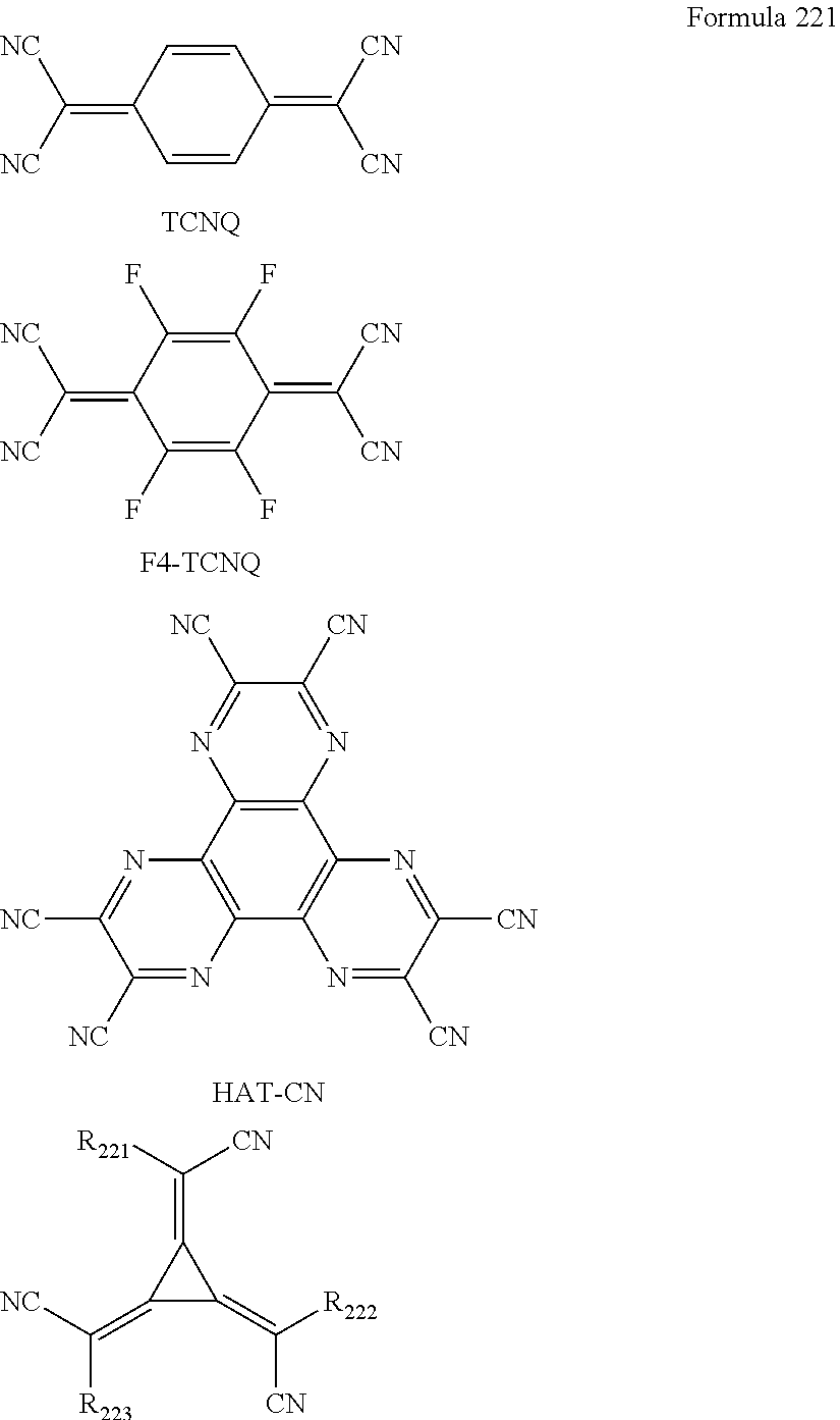


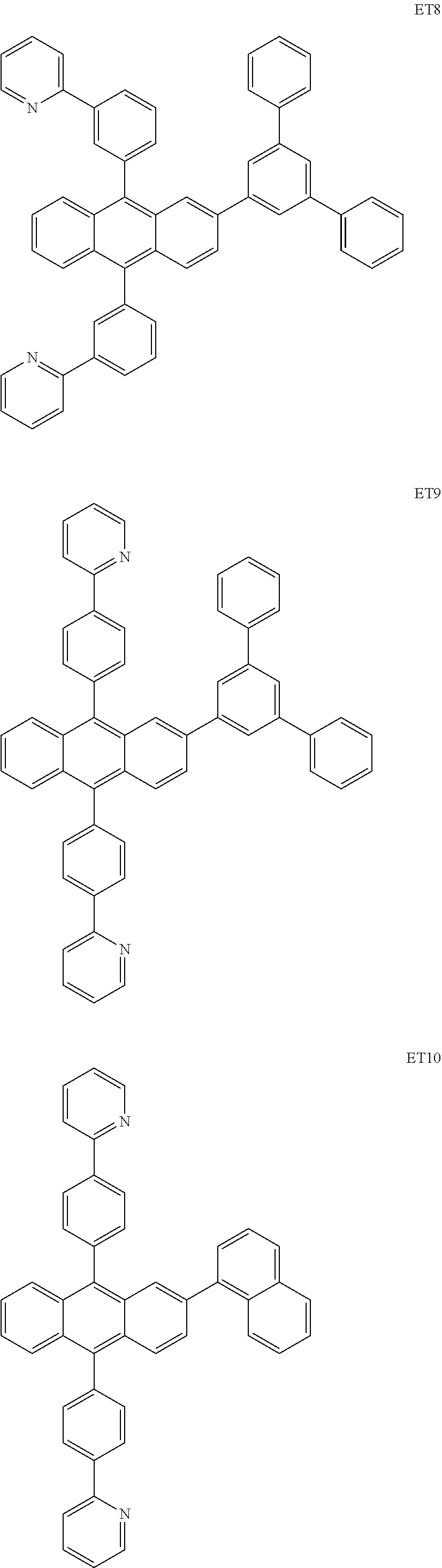


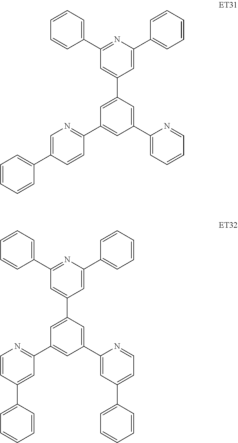


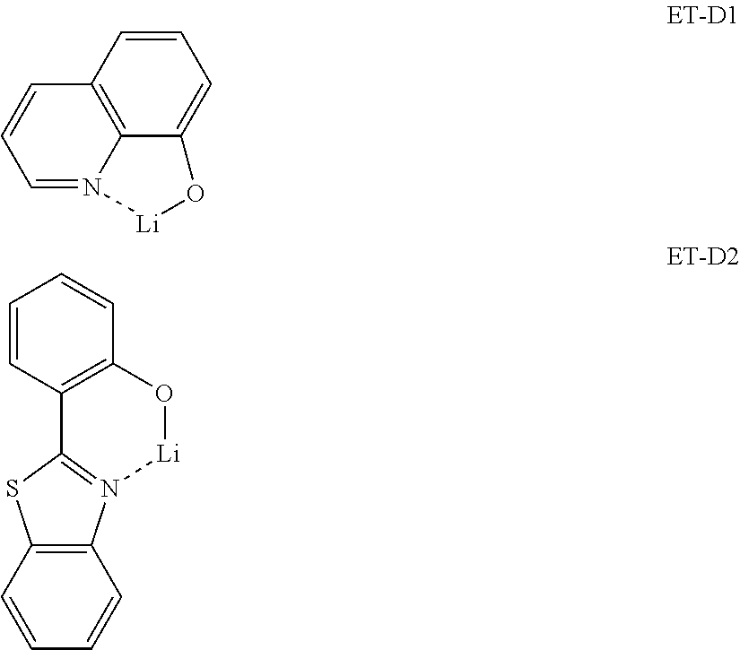


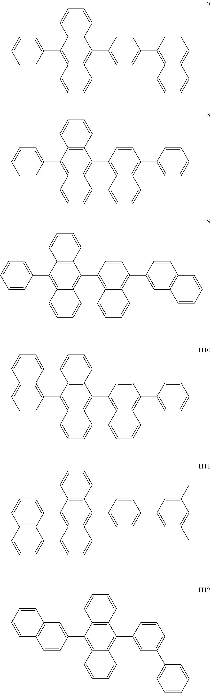


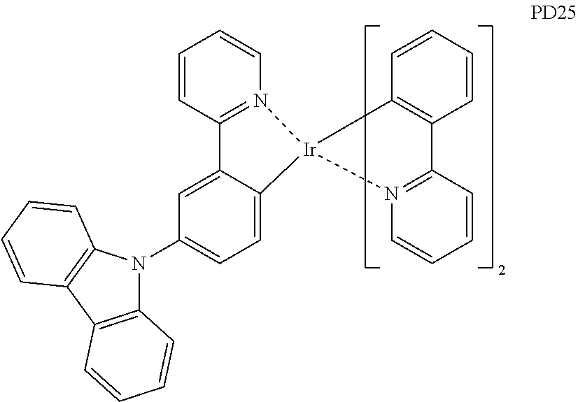

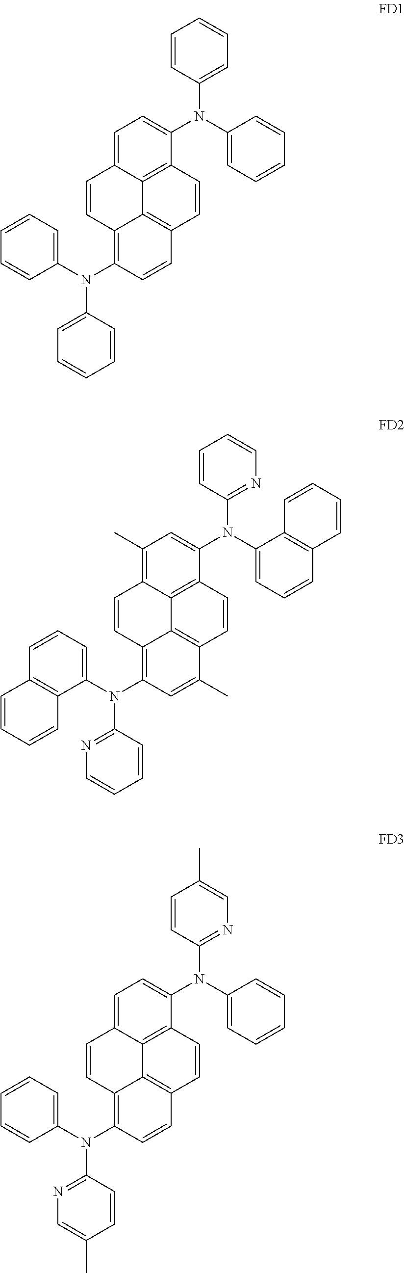


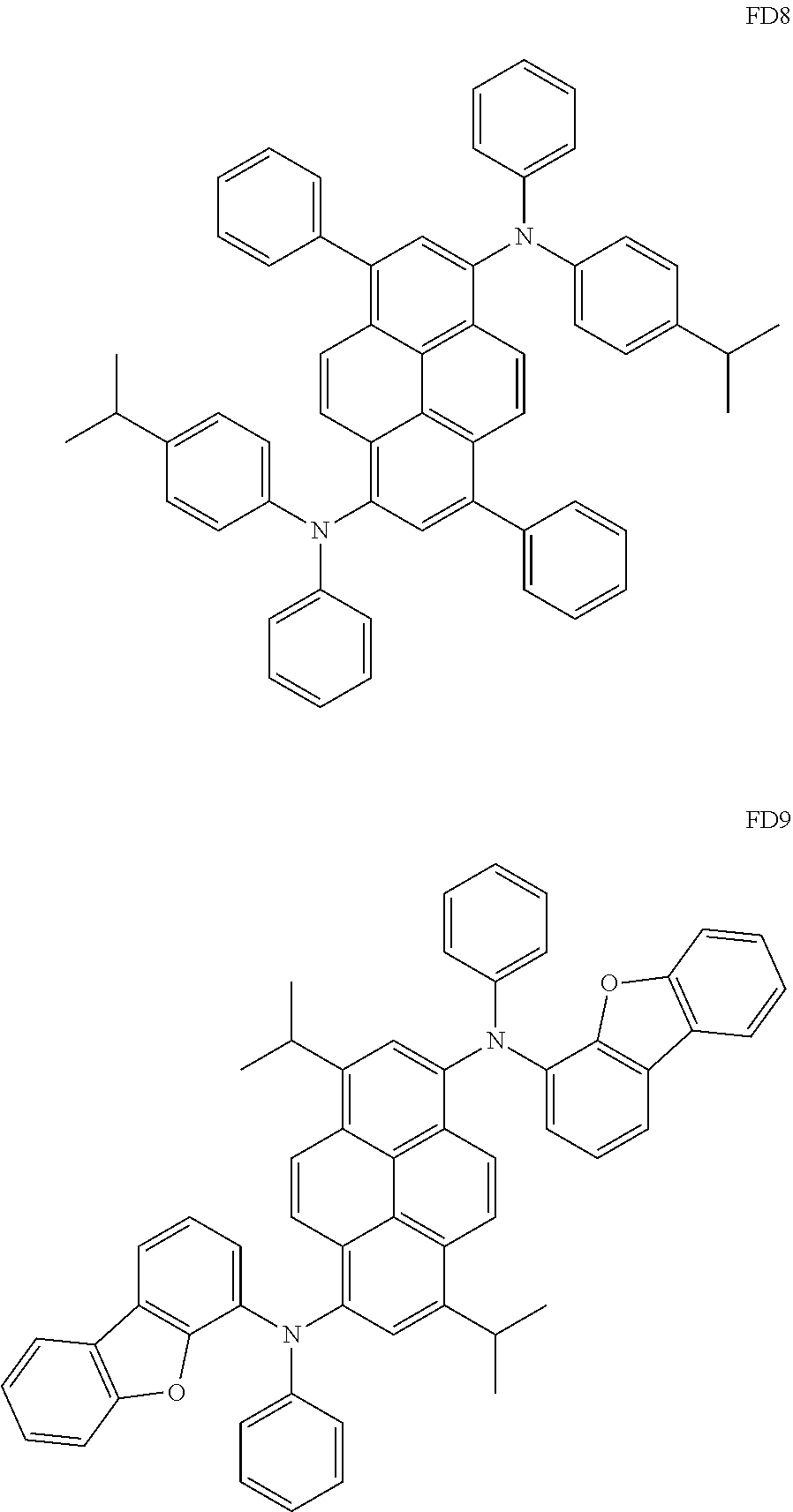


D00000
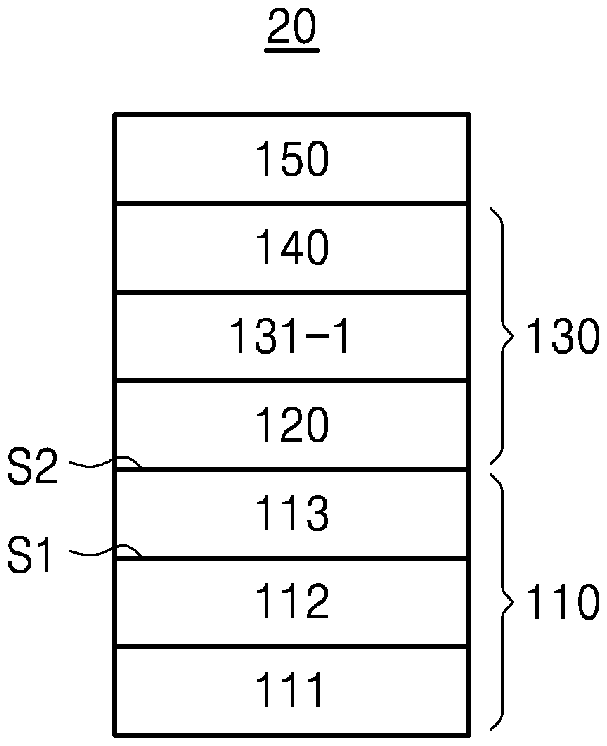
D00001
D00002
D00003

D00004
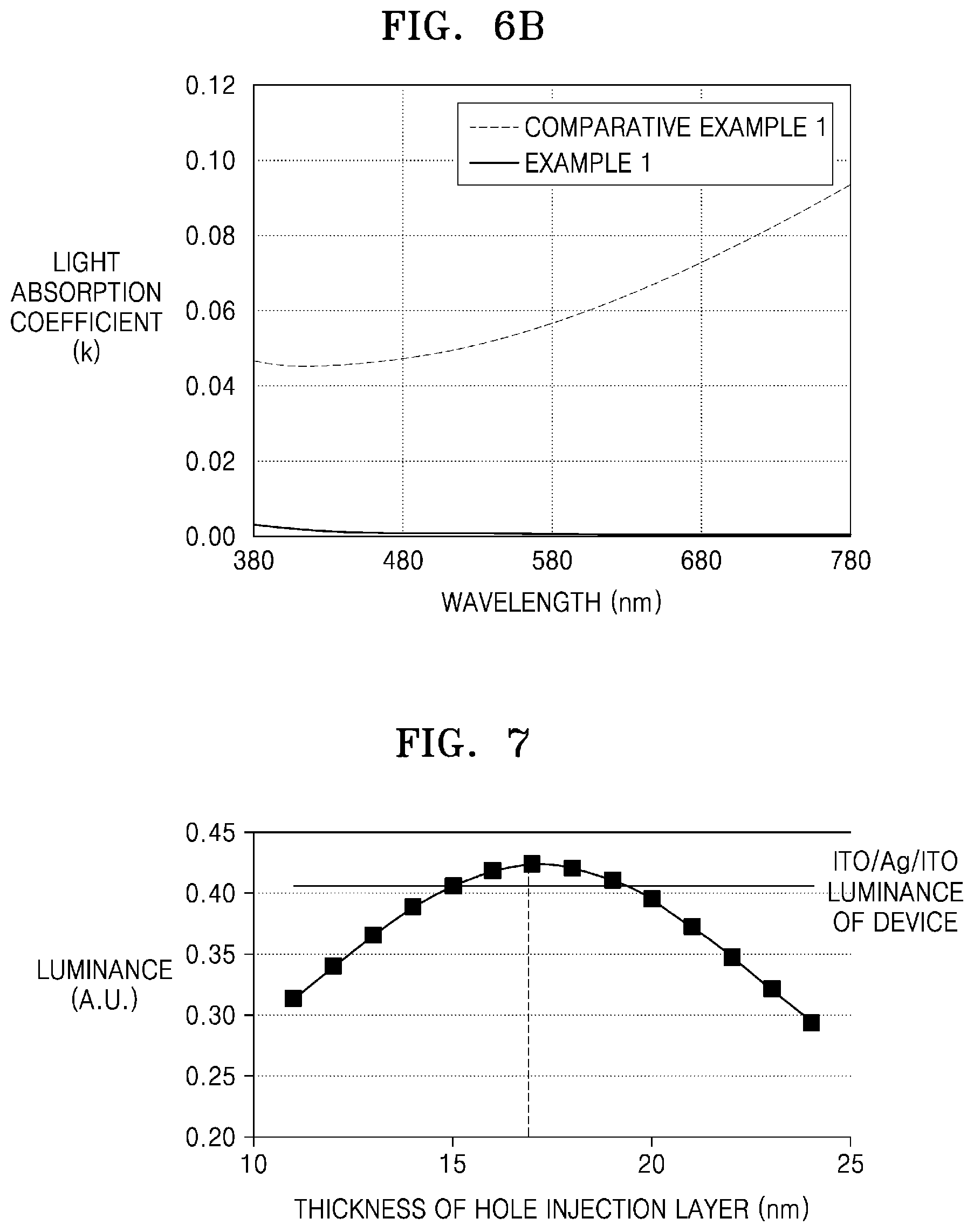
D00005


XML
uspto.report is an independent third-party trademark research tool that is not affiliated, endorsed, or sponsored by the United States Patent and Trademark Office (USPTO) or any other governmental organization. The information provided by uspto.report is based on publicly available data at the time of writing and is intended for informational purposes only.
While we strive to provide accurate and up-to-date information, we do not guarantee the accuracy, completeness, reliability, or suitability of the information displayed on this site. The use of this site is at your own risk. Any reliance you place on such information is therefore strictly at your own risk.
All official trademark data, including owner information, should be verified by visiting the official USPTO website at www.uspto.gov. This site is not intended to replace professional legal advice and should not be used as a substitute for consulting with a legal professional who is knowledgeable about trademark law.