Semiconductor Packaging Method And Semiconductor Structure
LIAO; Chuxian ; et al.
U.S. patent application number 17/452450 was filed with the patent office on 2022-04-28 for semiconductor packaging method and semiconductor structure. The applicant listed for this patent is CHANGXIN MEMORY TECHNOLOGIES, INC.. Invention is credited to Jun He, Chuxian LIAO, Jie Liu, Zhan Ying, Lixia Zhang.
| Application Number | 20220130726 17/452450 |
| Document ID | / |
| Family ID | 1000005974255 |
| Filed Date | 2022-04-28 |


View All Diagrams
| United States Patent Application | 20220130726 |
| Kind Code | A1 |
| LIAO; Chuxian ; et al. | April 28, 2022 |
SEMICONDUCTOR PACKAGING METHOD AND SEMICONDUCTOR STRUCTURE
Abstract
Embodiments of the present disclosure propose a semiconductor packaging method and a semiconductor structure. The semiconductor packaging method includes: providing a substrate; forming a metal pad on the substrate, where there is a gap between a sidewall of the metal pad and the substrate; and connecting multiple metal pads on substrates to each other.
| Inventors: | LIAO; Chuxian; (Hefei City, CN) ; Liu; Jie; (Hefei City, CN) ; He; Jun; (Hefei City, CN) ; Zhang; Lixia; (Hefei City, CN) ; Ying; Zhan; (Hefei City, CN) | ||||||||||
| Applicant: |
|
||||||||||
|---|---|---|---|---|---|---|---|---|---|---|---|
| Family ID: | 1000005974255 | ||||||||||
| Appl. No.: | 17/452450 | ||||||||||
| Filed: | October 27, 2021 |
Related U.S. Patent Documents
| Application Number | Filing Date | Patent Number | ||
|---|---|---|---|---|
| PCT/CN2021/110939 | Aug 5, 2021 | |||
| 17452450 | ||||
| Current U.S. Class: | 1/1 |
| Current CPC Class: | H01L 21/76898 20130101; H01L 24/94 20130101; H01L 23/53228 20130101; H01L 23/481 20130101 |
| International Class: | H01L 21/768 20060101 H01L021/768; H01L 23/48 20060101 H01L023/48; H01L 23/00 20060101 H01L023/00; H01L 23/532 20060101 H01L023/532 |
Foreign Application Data
| Date | Code | Application Number |
|---|---|---|
| Oct 22, 2020 | CN | 202011137752.4 |
Claims
1. A semiconductor packaging method, comprising: providing a substrate; forming a metal pad on the substrate, wherein there is a gap between a sidewall of the metal pad and the substrate; and connecting multiple metal pads on substrates to each other.
2. The semiconductor packaging method according to claim 1, wherein a method for forming the gap comprises: forming a groove in the substrate; forming a sacrificial material layer on a sidewall of the groove; forming the metal pad in the groove; and removing at least a part of the sacrificial material layer to form the gap.
3. The semiconductor packaging method according to claim 2, wherein a thickness of the sacrificial material layer at a position close to a surface of the substrate is greater than a thickness of the sacrificial material layer at a position away from the surface of the substrate.
4. The semiconductor packaging method according to claim 3, wherein the sacrificial material layer comprises any one of silicon oxide, silicon nitride, silicon oxynitride, or silicon oxycarbide; the sacrificial material layer is formed by plasma enhanced chemical vapor deposition (PECVD); and the PECVD is performed at a temperature of 100-200.degree. C., and a pressure of 10-30 Torr.
5. The semiconductor packaging method according to claim 3, wherein the sacrificial material layer comprises a metal material layer formed by physical vapor deposition (PVD); and the PVD is performed at a temperature of 50-350.degree. C., a flow rate of inert gas of 100-450 sccm, and a pressure of the inert gas of 0.1-10 Torr.
6. The semiconductor packaging method according to claim 2, wherein a thickness of the sacrificial material layer is one-thousandth to ten-thousandth of a size of the metal pad along a direction perpendicular to the sidewall of the groove.
7. The semiconductor packaging method according to claim 2, wherein the step of removing at least a part of the sacrificial material layer to form the gap comprises: removing at least a part of the sacrificial material layer by dry etching, wet etching, or chemical mechanical polishing (CMP).
8. The semiconductor packaging method according to claim 2, wherein the groove comprises a first groove and a second groove, the second groove is located below the first groove, and a size of an opening of the second groove is smaller than a size of a bottom of the first groove.
9. The semiconductor packaging method according to claim 8, wherein the step of forming the sacrificial material layer on the sidewall of the groove comprises: filling a first sacrificial layer in the second groove; forming a second sacrificial layer on the surface of the substrate, a sidewall of the first groove, the bottom of the first groove, and a surface of the first sacrificial layer; and removing a part of the second sacrificial layer which is on the surface of the substrate, on the bottom of the first groove, and on the surface of the first sacrificial layer, to retain the second sacrificial layer on the sidewall of the first groove as the sacrificial material layer.
10. The semiconductor packaging method according to claim 8, wherein the step of forming the sacrificial material layer on the sidewall of the groove comprises: forming a metal layer on the surface of the substrate, the bottom and a sidewall of the first groove, and a bottom and a sidewall of the second groove; and removing the metal layer on the surface of the substrate, the bottom of the first groove, and the bottom of the second groove, to retain the metal layer on the sidewall of the first groove and the sidewall of the second groove as the sacrificial material layer.
11. The semiconductor packaging method according to claim 10, wherein a material of the metal pad comprises copper; and a material of the metal layer comprises nickel, zinc, aluminum, silver, or gold.
12. The semiconductor packaging method according to claim 10, wherein a ratio of a length of the gap in a direction along the sidewall of the first groove to a length of the sidewall of the first groove is 0.1-0.5.
13. The semiconductor packaging method according to claim 8, wherein the step of removing at least a part of the sacrificial material layer to form the gap comprises: forming a metal layer on the surface of the substrate, the bottom and a sidewall of the first groove, and a bottom and a sidewall of the second groove; forming the metal pad in the groove; and removing a part of the metal layer on the surface of the substrate, and the sidewall of the first groove by CMP, to form the gap; wherein a thermal expansion coefficient of the metal layer is different from a thermal expansion coefficient of the metal pad.
14. The semiconductor packaging method according to claim 13, wherein a material of the metal pad comprises copper; and a material of the metal layer comprises magnesium, zinc, silver, aluminum, or gold.
15. The semiconductor packaging method according to claim 13, wherein a ratio of a length of the gap in a direction along the sidewall of the first groove to a length of the sidewall of the first groove is 0.01-0.1.
16. A semiconductor structure, comprising: a substrate with a groove; a metal pad located in the groove; and a gap, wherein at least a part of the gap is located on a sidewall of the groove, and the gap at least partially separates the metal pad from the substrate.
17. The semiconductor structure according to claim 16, wherein a width of an upper part of the gap is greater than a width of a lower part of the gap.
18. The semiconductor structure according to claim 16, wherein a cross-sectional profile of the groove in a direction along a surface of the substrate is in a sawtooth shape.
19. The semiconductor structure according to claim 16, wherein the groove comprises a first groove and a second groove, the second groove is located at a bottom of the first groove, and a size of an opening of the second groove is smaller than a size of the bottom of the first groove.
20. The semiconductor structure according to claim 19, wherein at least a part of the gap is located above a sidewall of the first groove.
Description
CROSS-REFERENCE TO RELATED APPLICATIONS
[0001] This is a continuation of International Patent Application No. PCT/CN2021/110939, filed on Aug. 5, 2021, which claims the priority to Chinese Patent Application No. 202011137752.4, titled "SEMICONDUCTOR PACKAGING METHOD AND SEMICONDUCTOR STRUCTURE" and filed on Oct. 22, 2020. The entire contents of International Patent Application No. PCT/CN2021/110939 and Chinese Patent Application No. 202011137752.4 are incorporated herein by reference.
TECHNICAL FIELD
[0002] The present disclosure relates to the field of semiconductors and semiconductor packaging technologies.
BACKGROUND
[0003] When a hybrid bonding technology is used to bond wafers to each other, because a metal pad has a higher thermal expansion coefficient than a dielectric layer on a surface of a wafer to be bonded, a dielectric layer near the metal pad will be bonded.
SUMMARY
[0004] One aspect of embodiments of the present disclosure provides a semiconductor packaging method, including: providing a substrate; forming a metal pad on the substrate, where there is a gap between a sidewall of the metal pad and the substrate; and connecting multiple metal pads on substrates to each other.
[0005] Another aspect of the embodiments of the present disclosure provides a semiconductor structure, including: a substrate with a groove; a metal pad located in the groove; and a gap, where at least a part of the gap is located on a sidewall of the groove, and the gap at least partially separates the metal pad from the substrate.
BRIEF DESCRIPTION OF THE DRAWINGS
[0006] The preferred embodiments of the present disclosure are described in detail below with reference to the accompanying drawings to make the objectives, features, and advantages of the present disclosure more obvious. The drawings are merely exemplary illustrations of the present disclosure, and are not necessarily drawn to scale. Same reference numerals in the drawings always represent same parts.
[0007] FIG. 1 to FIG. 9 are respectively schematic structural diagrams of a semiconductor structure in multiple steps of a semiconductor packaging method according to an exemplary implementation;
[0008] FIG. 10 is a top view of FIG. 6;
[0009] FIG. 11 to FIG. 18 are respectively schematic structural diagrams of a semiconductor structure in multiple steps of a semiconductor packaging method according to another exemplary implementation;
[0010] FIG. 19 is a top view of FIG. 15;
[0011] FIG. 20 to FIG. 27 are respectively schematic structural diagrams of a semiconductor structure in multiple steps of a semiconductor packaging method according to still another exemplary implementation;
[0012] FIG. 28 is a top view of FIG. 24;
[0013] FIG. 29 to FIG. 31 are respectively schematic structural diagrams of a semiconductor structure formed by using the semiconductor packaging method according to three exemplary implementations;
[0014] FIG. 32 is a schematic structural diagram of a sacrificial material layer formed in a semiconductor packaging method according to still another exemplary implementation; and
[0015] FIG. 33 is a schematic structural diagram of a sacrificial material layer formed in a semiconductor packaging method according to still another exemplary implementation.
DETAILED DESCRIPTION
[0016] Exemplary implementations will be described below in further detail with reference to the accompanying drawings. However, the exemplary implementations can be implemented in various forms, and should not be construed as being limited to those described herein. On the contrary, these exemplary implementations are provided to make the present disclosure comprehensive and complete and to fully convey the concept manifested therein to persons skilled in the art. Same reference numerals in the figures indicate same or similar structures, and thus their detailed descriptions will be omitted.
[0017] Implementation 1
[0018] FIG. 1 to FIG. 10 are respectively schematic structural diagrams of examples of a semiconductor structure in multiple steps of a semiconductor packaging method proposed in the present disclosure.
[0019] As shown in FIG. 1 to FIG. 10, in this implementation, the semiconductor packaging method proposed in the present disclosure includes the following steps.
[0020] Provide a substrate 100, where the substrate may be a wafer on which a semiconductor device is formed, a to-be-packaged semiconductor chip, or the like; the wafer may be a silicon wafer, a silicon carbide wafer, a SOI wafer, a gallium arsenide wafer, a gallium carbide wafer, a gallium nitride wafer, or the like; and the semiconductor device formed on the wafer may be a storage device such as a DRAM device or a NAND device, or may be a logic device such as a CPU device.
[0021] Form a metal pad 400 on the substrate 100, where there is a gap 510 between a sidewall of the metal pad 400 and the substrate 100. In an example, the metal pad 400 may be used for bonding different wafers, and a material of the metal pad 400 may include a conductive metal material such as copper, aluminum, gold, and silver.
[0022] Connect multiple metal pads 400 on substrates to each other. In an example, different wafers are bonded together by connecting metal pads 400 on different substrates to each other, to increase packaging density.
[0023] The gap is formed between the sidewall of the metal pad and the substrate. This can reduce damage caused by a metal pad between different substrates to a structure surrounding the metal pad during a bonding process due to thermal expansion, thereby achieving a better packaging effect.
[0024] Optionally, a method for forming the gap 510 includes: forming a groove 110 in the substrate 100; forming a sacrificial material layer 300 on a sidewall of the groove 110; forming the metal pad 400 in the groove 110; and removing at least a part of the sacrificial material layer 300 to form the gap 510.
[0025] Optionally, as shown in FIG. 1, the groove 110 may include a first groove 111 and a second groove 112. The second groove 112 is located below the first groove 111, and a size of an opening of the second groove 112 is smaller than that of a bottom of the first groove 111. Specifically, the first groove 111 may be an interconnection line groove in a Damascus process, the second groove 112 may be an interconnection hole groove in a Damascus process, and the interconnection hole groove is located below the interconnection line groove and is connected to the interconnection line groove. In a direction perpendicular to an extension direction of an interconnection line, a size of an opening of the interconnection hole groove is smaller than that of a bottom of the interconnection line groove. The size of the opening may be a size of the top part of the interconnection hole groove.
[0026] Optionally, as shown in FIG. 2 to FIG. 4, the step of forming a sacrificial material layer 300 on a sidewall of the groove 110 may include the following steps.
[0027] Fill a first sacrificial layer 311 in the second groove 112. Specifically, the first sacrificial layer 311 may be formed in the second groove 112 by using a chemical vapor deposition or spin coating process. A material of the first sacrificial layer 311 may include a material such as silicon oxide, silicon nitride, amorphous carbon, a spin-coated organic dielectric layer, or a spin-coated inorganic dielectric layer. For example, the formed first sacrificial layer 311 fully fills at least the second groove 112, such that a sidewall of the second groove 112 is fully covered, ensuring that the subsequently formed sacrificial material layer 300 does not exist on the sidewall of the second groove 112. This ensures a size of an interconnection hole formed in the second groove 112, and prevents an increase in a contact resistance.
[0028] Form a second sacrificial layer 312 on a surface of the substrate 100, a sidewall of the first groove 111, the bottom of the first groove 111, and a surface of the first sacrificial layer 311. Specifically, the second sacrificial layer 312 may be a material layer that is formed by using a chemical vapor deposition or atomic layer deposition process and that is different from the first sacrificial layer 311, and a material of the second sacrificial layer 312 may include a material such as silicon oxide, silicon nitride, silicon oxynitride, or silicon oxycarbide.
[0029] Remove the second sacrificial layer 312 on the surface of the substrate 100, the bottom of the first groove 111, and the surface of the first sacrificial layer 311 to retain the second sacrificial layer 312 on the sidewall of the first groove 111 as the sacrificial material layer 300. Specifically, the second sacrificial layer 312 which on the surface of the substrate 100, on the bottom of the first groove 111, and on the surface of the first sacrificial layer 311 may be removed by using a dry etching process, to retain the second sacrificial layer on the sidewall of the first groove 111.
[0030] In this way, a thickness of the formed sacrificial material layer can be controllable to control a characteristic of the subsequently formed gap, such as a size, a position, or a shape, such that it is possible to form a gap with a corresponding characteristic based on a bonding process condition or a material, a size, or the like of the metal pad. This fully reduces damage caused by a metal pad between substrates to a structure surrounding the metal pad during a bonding process due to thermal expansion, and ensures a bonding degree between the metal pad and the substrates, thereby achieving a better packaging effect.
[0031] Optionally, a thickness of the sacrificial material layer 300 is one-thousandth to ten-thousandth of a size of the metal pad 400 along a direction perpendicular to the sidewall of the groove. Specifically, the thickness of the sacrificial material layer 300 is a size of the sacrificial material layer along the direction perpendicular to the sidewall of the groove. When a bonding temperature of a metal pad 400 between different substrates is approximately 300.degree. C., a size of a gap formed by the sacrificial material layer 300 of the foregoing thickness can compensate for a size change of the metal pad 400 resulting from thermal expansion to a greatest extent.
[0032] Optionally, a thickness of the sacrificial material layer at a position close to a surface of the substrate is greater than a thickness of the sacrificial material layer at a position away from the surface of the substrate. As shown in FIG. 32, a thickness of a second sacrificial layer 312 at a position 312a close to the surface of the substrate 100 is greater than a thickness of the second sacrificial layer 312 at a position 312b away from the surface of the substrate 100. It should be understood that "close to" and "away from" are relative, and do not constitute limitations on specific positions. A gap formed by the sacrificial material layer with the foregoing morphology may well match an actual change of the metal pad 400 during bonding. During bonding of the metal pad 400, larger space is required near a position of a contact surface between different metal pads 400 to accommodate an expanded part. Specifically, the sacrificial material layer includes any one of silicon oxide, silicon nitride, silicon oxynitride, or silicon oxycarbide; the silicon oxide, the silicon nitride, the silicon oxynitride, and the silicon oxycarbide, the sacrificial material layer is formed by plasma enhanced chemical vapor deposition (PECVD). The PECVD is performed at a temperature of 100-200.degree. C., and a pressure of 10-30 Torr. The morphology of the sacrificial material layer formed in the conditions may well satisfy a requirement.
[0033] Optionally, before forming the first sacrificial layer 311 and the second sacrificial layer 312, the method further includes: forming a barrier layer 200 on sidewalls and bottoms of the first groove 111 and the second groove 112. As shown in FIG. 1, the barrier layer 200 is formed on the bottoms and the sidewalls of the first groove 111 and the second groove 112 by using an ALD process or another deposition process. A material of the barrier layer 200 may include titanium nitride (TiN). In another implementation, a material of the barrier layer 200 may alternatively include titanium (Ti), tantalum (Ta), tantalum nitride (TaN), ruthenium (Ru), rhenium (Re), conductive metal nitride, or the like. This is not limited to this implementation.
[0034] Optionally, the step of removing at least a part of the sacrificial material layer to form the gap includes:
[0035] removing at least a part of the sacrificial material layer by dry etching, wet etching, or chemical mechanical polishing (CMP). Specifically, the sacrificial material layer may be removed by dry etching or wet etching by using an etching selection ratio between the metal pad and the sacrificial material layer, and an etching degree may be controlled by time control or by using an etching end-point, to control a size of the formed gap. In an example, FIG. 10 is a top view of FIG. 6. The gap 510 surrounds the metal pad 400, and separates an upper part that is of the metal pad 400 and that is close to the surface of the substrate 100 from the substrate. In this example, a cross-sectional profile of the groove 110 in a direction along the surface of the substrate 100 is in a shape of a square. In another example, a cross-sectional profile of the groove 110 in a direction along the surface of the substrate 100 is in a sawtooth shape, such that a cross-sectional profile of the formed gap 510 in the direction along the surface of the substrate 100 is also in a sawtooth shape. This achieves an effect of releasing stress and reduces damage caused by the metal pad 400 to a structure surrounding the metal pad 400.
[0036] Optionally, as shown in FIG. 7 to FIG. 9, bonding two substrates 600, each substrate with a gap and a metal pad 400, may include the following steps:
[0037] aligning the substrates 600 each provided with a gap and a metal pad 400;
[0038] performing pre-bonding, for example, fusion bonding (fusion bond), on the metal pads 400 on the substrates 600; and
[0039] performing annealing (anneal) treatment on the bonded metal pads 400, such that the metal pads 400 expand to fill the gap 510.
[0040] Optionally, in the step of forming the groove 110, a longitudinal cross-section of the groove 110 may be set to be in a roughly trapezoidal shape, and a semiconductor structure obtained after bonding is roughly shown in FIG. 29. According to the foregoing design, a bonding area of the metal pad 400 can be further increased, so as to reduce a contact resistance.
[0041] Implementation 2
[0042] Based on the foregoing detailed description of the exemplary implementation of the semiconductor packaging method proposed in the present disclosure, another exemplary implementation of the semiconductor packaging method proposed in the present disclosure is described below with reference to FIG. 11 to FIG. 19. A part that is in this implementation and that is substantially the same as the related process in the foregoing first implementation is not described herein again.
[0043] Optionally, as shown in FIG. 12 and FIG. 13, in this implementation, the step of forming a sacrificial material layer 300 on a sidewall of the groove 110 may include the following steps.
[0044] Form a metal layer 320 on the surface of the substrate 100, the bottom and a sidewall of the first groove, and the bottom and a sidewall of the second groove.
[0045] Remove the metal layer 320 on the surface of the substrate 100, the bottom of the first groove, and the bottom of the second groove to retain the metal layer 320 on the sidewall of the first groove and the sidewall of the second groove as the sacrificial material layer 300.
[0046] According to the foregoing method, a fabrication process for forming the sacrificial material layer 300 is simplified, without increasing a contact resistance of an interconnection hole formed in the second groove.
[0047] Optionally, the metal layer 320 is formed by using a physical vapor deposition (PVD) process, and the PVD is performed at a temperature of 50-350.degree. C., a flow rate of inert gas of 100-450 sccm, and a pressure of the inert gas of 0.1-10 Torr. As shown in FIG. 33, a thickness that is of the material layer 300 formed by using the foregoing process and that is at a position 320a close to the surface of the substrate 100 is greater than a thickness of the material layer 300 at a position 320b away from the surface of the substrate 100. It should be understood that "close to" and "away from" are relative, and do not constitute limitations on specific positions.
[0048] Optionally, a material of the metal pad 400 includes copper, and a material of the metal layer 320 includes nickel, zinc, aluminum, silver, or gold.
[0049] Optionally, a ratio of a length of a gap 520 in a direction along the sidewall of the first groove to a length of the sidewall of the first groove is 0.1-0.5, for example, 0.1, 0.3, 0.4, and 0.5. FIG. 15 shows the substrate 100, the groove 110, a barrier layer 200, the sacrificial material layer 300, the metal pad 400, and the gap 520 in the semiconductor structure. The gap 520 is formed by removing a part of the sacrificial material layer 300, or in other words, the gap 520 is formed by a channel between a sidewall of the metal pad 400, the sidewall of the groove 110, and the remaining sacrificial material layer 300. FIG. 19 shows an example of a top view of FIG. 15. It can be seen that the gap 520 surrounds the metal pad 400.
[0050] FIG. 16 to FIG. 18 are respectively examples of schematic structural diagrams of a semiconductor structure in several steps of "bonding two substrates 600". The process of bonding the two substrates 600 in this implementation is roughly the same as the related process in the foregoing first implementation, and details are not described herein again.
[0051] In addition, based on the foregoing design in the implementation shown in FIG. 11 to FIG. 19, in another implementation, in the step of forming the groove, a longitudinal cross-section of the groove may be set to be in a roughly trapezoidal shape, and a semiconductor structure obtained after bonding is roughly shown in FIG. 30. According to the foregoing design, a bonding area of the metal pad 400 can be further increased, so as to reduce a contact resistance.
[0052] Implementation 3
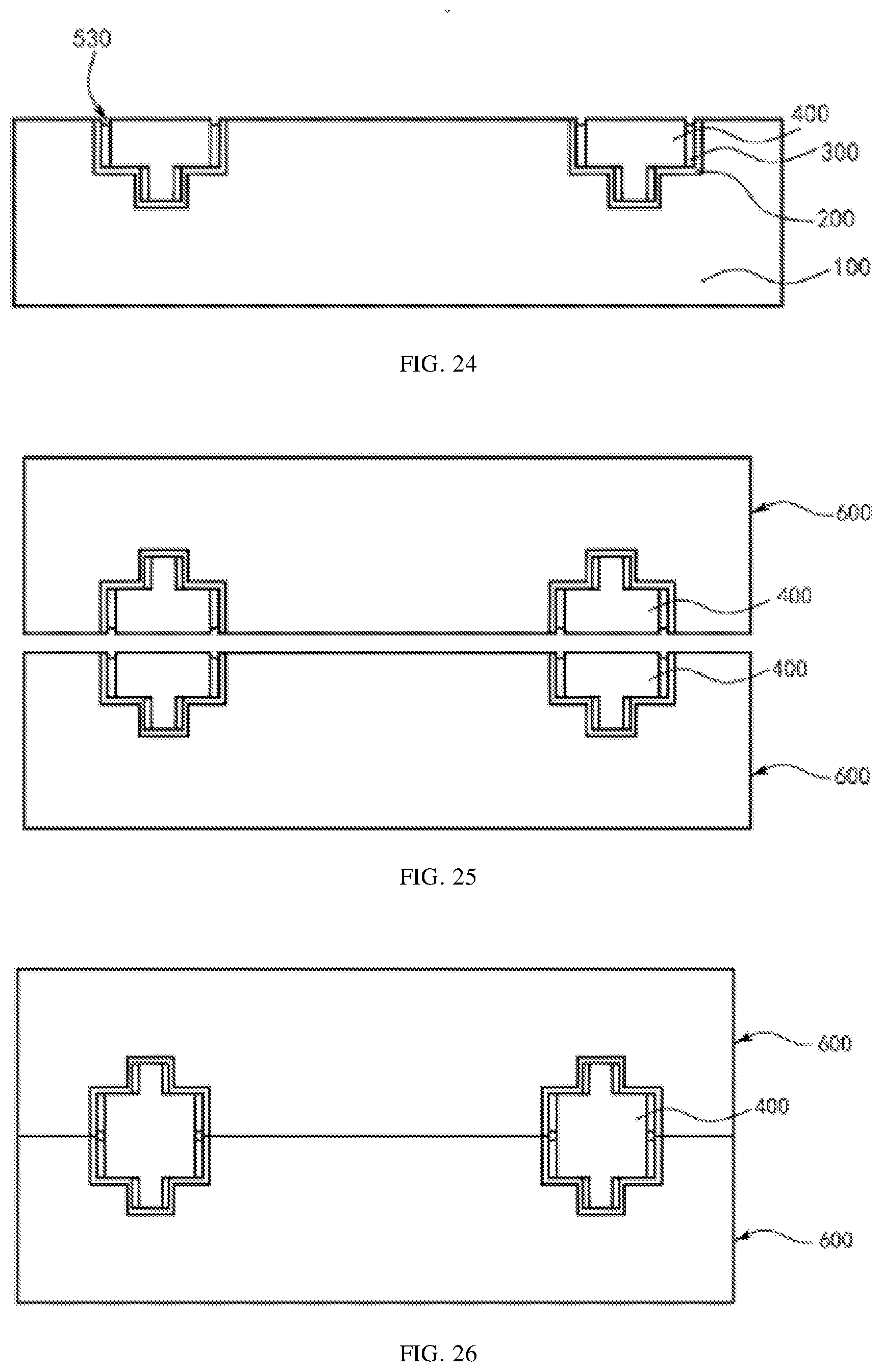
[0053] Based on the foregoing detailed description of the two exemplary implementations of the semiconductor packaging method proposed in the present disclosure, still another exemplary implementation of the semiconductor packaging method proposed in the present disclosure is described below with reference to FIG. 20 to FIG. 28. A part that is in this implementation and that is substantially the same as the related process in the foregoing first implementation and/or the second embodiment is not described herein again.
[0054] Optionally, as shown in FIG. 21 and FIG. 24, a step of removing at least a part of the sacrificial material layer 300 to form a gap 530 includes the following steps:
[0055] Form a metal layer 330 on the surface of the substrate 100, the bottom and the sidewall of the first groove, and the bottom and a sidewall of the second groove, and remove a part of the metal layer 330 on the surface of the substrate 100, the bottom of the first groove, and the bottom of the second groove to retain the metal layer 330 on the sidewall of the first groove as the sacrificial material layer 300.
[0056] Form the metal pad 400 in the groove 110.
[0057] Remove a part of the sacrificial material layer 300 on the surface of the substrate 100 and the sidewall of the first groove by CMP to form the gap 530. A thermal expansion coefficient of the sacrificial material layer 300 is different from a thermal expansion coefficient of the metal pad 400, to prevent the remaining sacrificial material layer on the sidewall of the first groove from causing damage to a structure surrounding the metal pad due to thermal expansion in the bonding process of the metal pad. For example, the thermal expansion coefficient of the sacrificial material layer 300 is less than that of the metal pad 400. Further, based on the foregoing design of the process of forming the sacrificial material layer 300, in this implementation, when the material of the metal pad 400 includes copper (Cu), the material of the sacrificial material layer 300 may include magnesium (Mg). In another implementation, the material of the sacrificial material layer 300 may alternatively include another material, for example, zinc (Zn), silver (Ag), aluminum (Al), or gold (Au). No limitation is set to this implementation. In this implementation, a process condition of chemical mechanical grinding, for example, a type of grinding liquid, is adjusted to selectively increase a grinding rate of the sacrificial material layer 300 to form the gap 530. FIG. 28 shows an example of a top view of FIG. 24. It can be seen that the gap 530 surrounds the metal pad 400.
[0058] Optionally, a ratio of a length of the gap 530 in a direction along the sidewall of the first groove to a length of the sidewall of the first groove is 0.01-0.1. For example, in this implementation, a ratio of a depth of the gap 530 formed by chemical mechanical grinding to a groove depth of the first groove may be 0.01-0.1, for example, 0.01, 0.04, 0.07, or 0.1. Based on the foregoing process design in this implementation, in another implementation, the ratio may alternatively be less than 0.01 or greater than 0.1, for example, 0.008 or 0.11. No limitation is set to this implementation.
[0059] FIG. 25 to FIG. 27 are respectively schematic diagrams of examples of schematic structural diagrams of a semiconductor structure in several steps of "bonding two substrates 600". The process of bonding the two substrates 600 in this implementation is roughly the same as the related processes in the foregoing first implementation and second implementation, and details are not described herein again.
[0060] In addition, based on the foregoing design in the implementation shown in FIG. 20 to FIG. 28, in another implementation, in the step of forming the groove 110, a longitudinal cross-section of the groove 110 may be set to be in a roughly trapezoidal shape, and a semiconductor structure obtained after bonding is roughly shown in FIG. 31. According to the foregoing design, a bonding area of the metal pad 400 can be further increased, so as to reduce a contact resistance.
[0061] Based on the foregoing detailed description of the multiple exemplary implementations of the semiconductor packaging method proposed in the present disclosure, an exemplary implementation of a semiconductor structure proposed in the present disclosure is described. The semiconductor structure in this embodiment may be fabricated by using the foregoing semiconductor packaging method that is proposed in the present disclosure and that is described in detail in the foregoing implementations.
[0062] As shown in FIG. 1 to FIG. 6, the semiconductor structure proposed in the present disclosure includes: the substrate 100 provided with the groove 110; the metal pad 400 located in the groove 110; and the gap 510, where at least a part of the gap 510 is located on a sidewall of the groove 110 and separates the metal pad 400 from at least a part of the substrate 100.
[0063] Optionally, a width of an upper part of the gap 510 is greater than that of a lower part of the gap.
[0064] Optionally, a cross-sectional profile of the groove 110 in a direction along the surface of the substrate 100 is in a sawtooth shape.
[0065] Optionally, the groove 110 includes the first groove 111 and the second groove 112, the second groove 112 is located at the bottom of the first groove 111, and a size of an opening of the second groove 112 is smaller than that of a bottom of the first groove 111.
[0066] Optionally, at least a part of the gap 510 is located above the sidewall of the first groove 111.
[0067] In conclusion, according to the semiconductor packaging method provided in the embodiments of the present disclosure, the sacrificial material layer is formed on the sidewall of the groove on the substrate, and after a conducting layer is formed, at least a part of the sacrificial material layer is removed to form the groove surrounding the conducting layer. According to the foregoing design, the semiconductor packaging method proposed in the embodiments of the present disclosure can implement a more controllable gap formation process, and reduce stress exerted by the metal pad formed by the conducting layer to a structure surrounding the metal pad during expansion in a subsequent fabrication process, thereby achieving a better packaging effect.
[0068] Although the present disclosure is described above with reference to several typical embodiments, it should be understood that the terms used herein are intended for illustration, rather than limiting. The present disclosure may be specifically implemented in many forms without departing from the spirit or essence of the present disclosure. Therefore, it should be understood that the above embodiments are not limited to any of the above-mentioned details, but should be broadly interpreted according to the spirit and scope defined by the appended claims. Therefore, any changes and modifications falling within the claims or the equivalent scope thereof should be covered by the appended claims.
* * * * *
D00000
D00001
D00002
D00003
D00004
D00005
D00006
D00007
D00008
D00009
D00010
D00011
D00012

XML
uspto.report is an independent third-party trademark research tool that is not affiliated, endorsed, or sponsored by the United States Patent and Trademark Office (USPTO) or any other governmental organization. The information provided by uspto.report is based on publicly available data at the time of writing and is intended for informational purposes only.
While we strive to provide accurate and up-to-date information, we do not guarantee the accuracy, completeness, reliability, or suitability of the information displayed on this site. The use of this site is at your own risk. Any reliance you place on such information is therefore strictly at your own risk.
All official trademark data, including owner information, should be verified by visiting the official USPTO website at www.uspto.gov. This site is not intended to replace professional legal advice and should not be used as a substitute for consulting with a legal professional who is knowledgeable about trademark law.