Inorganic Metal Halide Compound, A Method Of Manufacturing The Same, And An Optical Member, A Light-emitting Device, And An Apparatus, Each Including The Inorganic Metal Halide Compound
Chang; Jaebok ; et al.
U.S. patent application number 17/504190 was filed with the patent office on 2022-04-28 for inorganic metal halide compound, a method of manufacturing the same, and an optical member, a light-emitting device, and an apparatus, each including the inorganic metal halide compound. The applicant listed for this patent is Samsung Display Co., Ltd.. Invention is credited to Jaebok Chang, Maksym V. Kovalenko, Baekhee Lee, Junwoo Lee, Taekjoon Lee, Viktoriia Morad, Duckjong Suh.
| Application Number | 20220127529 17/504190 |
| Document ID | / |
| Family ID | |
| Filed Date | 2022-04-28 |


View All Diagrams
| United States Patent Application | 20220127529 |
| Kind Code | A1 |
| Chang; Jaebok ; et al. | April 28, 2022 |
INORGANIC METAL HALIDE COMPOUND, A METHOD OF MANUFACTURING THE SAME, AND AN OPTICAL MEMBER, A LIGHT-EMITTING DEVICE, AND AN APPARATUS, EACH INCLUDING THE INORGANIC METAL HALIDE COMPOUND
Abstract
An inorganic metal halide compound for one of a light emitting device and an optical member, the compound being represented by Formula 1 and having a double perovskite structure of Formula 1 as defined herein.
| Inventors: | Chang; Jaebok; (Yongin-si, KR) ; Kovalenko; Maksym V.; (Zurich, CH) ; Morad; Viktoriia; (Zurich, CH) ; Suh; Duckjong; (Yongin-si, KR) ; Lee; Baekhee; (Yongin-si, KR) ; Lee; Junwoo; (Yongin-si, KR) ; Lee; Taekjoon; (Yongin-si, KR) | ||||||||||
| Applicant: |
|
||||||||||
|---|---|---|---|---|---|---|---|---|---|---|---|
| Appl. No.: | 17/504190 | ||||||||||
| Filed: | October 18, 2021 |
| International Class: | C09K 11/75 20060101 C09K011/75; C01G 30/00 20060101 C01G030/00; H01L 27/32 20060101 H01L027/32; H01L 51/50 20060101 H01L051/50 |
Foreign Application Data
| Date | Code | Application Number |
|---|---|---|
| Oct 23, 2020 | KR | 10-2020-0138598 |
Claims
1. An inorganic metal halide compound represented by Formula 1 and having a double perovskite structure, in which: (A).sub.2(M.sup.1)(M.sup.3)(X).sub.6:Z Formula 1 wherein, in Formula 1, A and M.sup.1 are each, independently from one another, a monovalent inorganic cation, wherein M.sup.1 is not Na.sup.+ and A and M.sup.1 are different from each other, M.sup.3 is a trivalent metal-cation, X is a halide anion, and Z is bismuth or a metalloid, doped in (A).sub.2(M.sup.1)(M.sup.3)(X).sub.6.
2. The inorganic metal halide compound of claim 1, wherein A has a greater atomic radius than M.sup.1.
3. The inorganic metal halide compound of claim 1, wherein M.sup.1 is K.sup.+.
4. The inorganic metal halide compound of claim 1, wherein M.sup.3 is a post-transition metal ion.
5. The inorganic metal halide compound of claim 1, wherein X is F.sup.-, Cl.sup.+, Br.sup.-, or I.sup.-.
6. The inorganic metal halide compound of claim 1, wherein, a ratio Z/M.sup.3 of a number of moles of Z to a number of moles of M.sup.3 is greater than 0% and less than or equal to about 20%.
7. The inorganic metal halide compound of claim 1, wherein the double perovskite structure comprises a tetragonal structure.
8. The inorganic metal halide compound of claim 1, wherein a full width at half maximum of the inorganic metal halide compound is about 35 nm to about 130 nm.
9. The inorganic metal halide compound of claim 1, wherein a maximum emission wavelength of the inorganic metal halide compound is about 490 nm to about 570 nm.
10. The inorganic metal halide compound of claim 1, wherein a photoluminescence quantum yield of the inorganic metal halide compound is about 50% to about 100%.
11. The inorganic metal halide compound of claim 1, wherein an average particle size D50 of the inorganic metal halide compound is about 1 nm to about 100 nm.
12. A method of manufacturing an inorganic metal halide compound represented by Formula 1 and having a double perovskite structure, wherein the method comprises the steps of: obtaining a first solution by stirring a precursor of A and a precursor of M.sup.1; obtaining a second solution by stirring a precursor of M.sup.3 and a precursor of Z; and mixing the first solution and the second solution, to make the inorganic metal halide compound; (A).sub.2(M.sup.1)(M.sup.3)(X).sub.6:Z Formula 1 wherein, in Formula 1, A and M.sup.1 are each, independently from one another, a monovalent inorganic-cation, wherein M.sup.1 is not Na.sup.+ and A and M.sup.1 are different from each other, M.sup.3 is a trivalent metal-cation, X is a halide anion, and Z is bismuth or a metalloid, doped in (A).sub.2(M.sup.1)(M.sup.3)(X).sub.6.
13. A light-emitting device, wherein the light-emitting device comprises: a first electrode; a second electrode facing the first electrode; an interlayer between the first electrode and the second electrode and comprising an emission layer, wherein the interlayer comprises the inorganic metal halide compound of claim 1.
14. An optical member comprising the inorganic metal halide compound of claim 1.
15. The optical member of claim 14, wherein the optical member comprises a color conversion member.
16. The optical member of claim 15, wherein the color conversion member comprises a substrate and a pattern layer disposed on the substrate, and the pattern layer comprises the inorganic metal halide compound.
17. An apparatus, wherein the apparatus comprises the inorganic metal halide compound of claim 1.
18. The apparatus of claim 17, further comprising a light source, wherein the inorganic metal halide compound is located in a path of light emitted from the light source.
19. The apparatus of claim 18, wherein the light source comprises an organic light-emitting device or a light-emitting diode.
20. The apparatus of claim 17, wherein the apparatus comprises a photovoltaic device, a photodiode, a phototransistor, a photomultiplier, a photoresistor, a photodetector, a light-sensitive detector, a solid-state triode, a battery electrode, a light-emitting device, a transistor, a solar battery, a laser, or a diode injection laser.
Description
CROSS-REFERENCE TO RELATED APPLICATION
[0001] This application claims priority from and the benefit of Korean Patent Application No. 10-2020-0138598, filed on Oct. 23, 2020, which is hereby incorporated by reference for all purposes as if fully set forth herein.
BACKGROUND
Field
[0002] Embodiments of the invention relate generally to an inorganic metal halide is compound and, more specifically, to a method of manufacturing the same, and an optical member, a light-emitting device, and an apparatus, each including the inorganic metal halide compound.
Discussion of the Background
[0003] Luminescent materials may be classified into photoluminescence (PL) by light and electroluminescence (EL) by current according to their excitation mechanism, and may be classified into organic luminescent materials (fluorescent dyes, organic light-emitting device (OLED) phosphorescent materials, etc.) and inorganic luminescent materials (quantum dots, perovskite nanocrystals, etc.) according to their components.
[0004] In the case of organic luminescent materials, although the degree of absorption is good, there are drawbacks in terms of stability and color tuning, and although quantum dots may implement various colors by adjusting the particle size according to a quantum confinement effect, with smaller sizes the wavelengths are shorter, and thus, the degree of absorption of incident light decreases.
[0005] Also, the perovskite nanocrystals having lead (Pb) as a central metal have excellent luminescence characteristics due to defect tolerance photophysics, but are toxic. Even if there was an attempt to replace the central metal of the perovskite nanocrystals with another metal that is less toxic than lead, substitution of the central metal is limited due to characteristics of the crystal structure, and the perovskite nanocrystals do not exhibit high-efficiency luminescence characteristics as much as a case where the central metal is lead.
[0006] The above information disclosed in this Background section is only for understanding of the background of the inventive concepts, and, therefore, it may contain information that does not constitute prior art.
SUMMARY
[0007] Applicant recognized that there is a great need for a new material having crystal structures similar to the perovskite structure discussed above that does not include an environmental regulatory material and has high-efficiency luminescence characteristics.
[0008] Inorganic metal halide compounds and light-emitting devices including such compounds constructed according to principles and illustrative implementations of the invention, a method of manufacturing the same, and an apparatus including the inorganic metal compound are capable of providing an inorganic metal compound that has a double perovskite structure, does not include an environmental regulatory material, and has unexpected synergistic improvements in high-efficiency luminescence characteristics.
[0009] Additional features of the inventive concepts will be set forth in the description which follows, and in part will be apparent from the description, or may be learned by practice of the inventive concepts.
[0010] According to one aspect of the invention, an inorganic metal halide compound for one of light emitting device and optical member, the compound being represented by Formula 1 and having a double perovskite structure:
(A).sub.2(M.sup.1)(M.sup.3)(X).sub.6:Z Formula 1
wherein, in Formula 1, A and M.sup.1 may be each, independently from one another, a monovalent inorganic cation, wherein M.sup.1 may be not Na.sup.+ and A and M.sup.1 are different from each other, M.sup.3 may be a trivalent metal-cation, X may be a halide anion, and Z may be bismuth or a metalloid, doped in (A).sub.2(M.sup.1)(M.sup.3)(X).sub.6.
[0011] The A may have a greater atomic radius than M.sup.1.
[0012] The M.sup.1 may be K.sup.+.
[0013] The M.sup.3 may be a post-transition metal ion.
[0014] The X may be F.sup.-, Cl.sup.-, Br.sup.-, or I.sup.-.
[0015] A ratio Z/M.sup.3 of a number of moles of Z to a number of moles of M.sup.3 may be greater than 0% and less than or equal to about 20%.
[0016] The double perovskite structure may include a tetragonal structure.
[0017] A full width at half maximum of the inorganic metal halide compound may be about 35 nm to about 130 nm.
[0018] A maximum emission wavelength of the inorganic metal halide compound may be about 490 nm to about 570 nm.
[0019] A photoluminescence quantum yield of the inorganic metal halide compound may be about 50% to about 100%.
[0020] An average particle size D50 of the inorganic metal halide compound may be about 1 nm to about 100 nm.
[0021] According to another aspect of the invention, a method of manufacturing an inorganic metal halide compound represented by Formula 1 and having a double perovskite structure includes the steps of:
obtaining a first solution by stirring a precursor of A and a precursor of M.sup.1; obtaining a second solution by stirring a precursor of M.sup.3 and a precursor of Z; and mixing the first solution and the second solution, to make the inorganic metal halide compound of;
(A).sub.2(M.sup.1)(M.sup.3)(X).sub.6:Z Formula 1
wherein, in Formula 1,
[0022] A and M.sup.1 are each, independently from one another, a monovalent inorganic-cation, wherein M.sup.1 is not Na.sup.+ and A and M.sup.1 are different from each other,
M.sup.3 is a trivalent metal-cation, X is a halide anion, and Z is bismuth or a metalloid, doped in (A).sub.2(M.sup.1)(M.sup.3)(X).sub.6.
[0023] A light-emitting device may include: a first electrode; a second electrode facing the first electrode; an interlayer between the first electrode and the second electrode and including an emission layer, wherein the interlayer may include the inorganic metal halide compound of claim 1.
[0024] An optical member may include the inorganic metal halide compound of claim 1.
[0025] The optical member may include a color conversion member.
[0026] The color conversion member may include a substrate and a pattern layer disposed on the substrate, and the pattern layer may include the inorganic metal halide compound.
[0027] An apparatus may include the inorganic metal halide compound of claim 1.
[0028] The apparatus may include a light source, wherein the inorganic metal halide compound may be located in a path of light emitted from the light source.
[0029] The light source may include an organic light-emitting device or a light-emitting diode.
[0030] The apparatus may include a photovoltaic device, a photodiode, a phototransistor, a photomultiplier, a photoresistor, a photodetector, a light-sensitive detector, a solid-state triode, a battery electrode, a light-emitting device, a transistor, a solar battery, a laser, or a diode injection laser.
[0031] It is to be understood that both the foregoing general description and the following detailed description are illustrative and explanatory and are intended to provide further explanation of the invention as claimed.
BRIEF DESCRIPTION OF THE DRAWINGS
[0032] The accompanying drawings, which are included to provide a further understanding of the invention and are incorporated in and constitute a part of this specification, illustrate illustrative embodiments of the invention, and together with the description serve to explain the inventive concepts.
[0033] FIG. 1 is a schematic diagram illustrating a perovskite crystal structure of the related art.
[0034] FIG. 2 is a schematic diagram illustrating a comparison of a crystal structure of Cs.sub.2NaInCl.sub.6 of the related art and a structure of an embodiment of an inorganic metal halide compound (Cs.sub.2KInCl.sub.6) made according to the principles of the invention.
[0035] FIG. 3A and FIG. 3B are graphical depictions of measured normalized photoluminescence (PL) and photoluminescence excitation (PLE) spectra of Comparative example 1 and Synthesis Example 1 made according to the principles of the invention.
[0036] FIG. 4 is a graphical depiction of a photoluminescence quantum yield (PLQY) of Synthesis Examples 1 to 4 made according to the principles of the invention and Comparative Examples 1 to 4.
[0037] FIG. 5 is a schematic cross-sectional view of an embodiment of a light-emitting device constructed according to the principles of the invention.
[0038] FIG. 6 and FIG. 7 are cross-sectional views of embodiments of a light-emitting apparatus constructed according to of the principles of the invention.
DETAILED DESCRIPTION
[0039] In the following description, for the purposes of explanation, numerous specific details are set forth in order to provide a thorough understanding of various embodiments or implementations of the invention. As used herein "embodiments" and "implementations" are interchangeable words that are non-limiting examples of devices or methods employing one or more of the inventive concepts disclosed herein. It is apparent, however, that various embodiments may be practiced without these specific details or with one or more equivalent arrangements. In other instances, well-known structures and devices are shown in block diagram form in order to avoid unnecessarily obscuring various embodiments. Further, various embodiments may be different, but do not have to be exclusive. For example, specific shapes, configurations, and characteristics of an embodiment may be used or implemented in another embodiment without departing from the inventive concepts.
[0040] Unless otherwise specified, the illustrated embodiments are to be understood as providing illustrative features of varying detail of some ways in which the inventive concepts may be implemented in practice. Therefore, unless otherwise specified, the features, components, modules, layers, films, plates, panels, regions, and/or aspects, etc. (hereinafter individually or collectively referred to as "elements"), of the various embodiments may be otherwise combined, separated, interchanged, and/or rearranged without departing from the inventive concepts.
[0041] The use of cross-hatching and/or shading in the accompanying drawings is generally provided to clarify boundaries between adjacent elements. As such, neither the presence nor the absence of cross-hatching or shading conveys or indicates any preference or requirement for particular materials, material properties, dimensions, proportions, commonalities between illustrated elements, and/or any other characteristic, attribute, property, etc., of the elements, unless specified. Further, in the accompanying drawings, the size and relative sizes of elements may be exaggerated for clarity and/or descriptive purposes. When an embodiment may be implemented differently, a specific process order may be performed differently from the described order. For example, two consecutively described processes may be performed substantially at the same time or performed in an order opposite to the described order. Also, like reference numerals denote like elements.
[0042] When an element or, a layer, is referred to as being "on," "connected to," or "coupled to" another element or layer, it may be directly on, connected to, or coupled to the other element or layer or intervening elements or layers may be present. When, however, an element or layer is referred to as being "directly on," "directly connected to," or "directly coupled to" another element or layer, there are no intervening elements or layers present. To this end, the term "connected" may refer to physical, electrical, and/or fluid connection, with or without intervening elements. Further, the D1-axis, the D2-axis, and the D3-axis are not limited to three axes of a rectangular coordinate system, such as the x, y, and z-axes, and may be interpreted in a broader sense. For example, the D1-axis, the D2-axis, and the D3-axis may be perpendicular to one another, or may represent different directions that are not perpendicular to one another. For the purposes of this disclosure, "at least one of X, Y, and Z" and "at least one selected from the group consisting of X, Y, and Z" may be construed as X only, Y only, Z only, or any combination of two or more of X, Y, and Z, such as, for instance, XYZ, XYY, YZ, and ZZ. As used herein, the term "and/of" includes any and all combinations of one or more of the associated listed items.
[0043] Although the terms "first," "second," etc. may be used herein to describe various types of elements, these elements should not be limited by these terms. These terms are used to distinguish one element from another element. Thus, a first element discussed below could be termed a second element without departing from the teachings of the disclosure.
[0044] Spatially relative terms, such as "beneath," "below," "under," "lower," "above," "upper," "over," "higher," "side" (e.g., as in "sidewall"), and the like, may be used herein for descriptive purposes, and, thereby, to describe one elements relationship to another element(s) as illustrated in the drawings. Spatially relative terms are intended to encompass different orientations of an apparatus in use, operation, and/or manufacture in addition to the orientation depicted in the drawings. For example, if the apparatus in the drawings is turned over, elements described as "below" or "beneath" other elements or features would then be oriented "above" the other elements or features. Thus, the term "below" can encompass both an orientation of above and below. Furthermore, the apparatus may be otherwise oriented (e.g., rotated 90 degrees or at other orientations), and, as such, the spatially relative terms used herein interpreted accordingly.
[0045] The terminology used herein is for the purpose of describing particular embodiments and is not intended to be limiting. As used herein, the singular forms, "a," "an," and "the" are intended to include the plural forms as well, unless the context clearly indicates otherwise. Moreover, the terms "comprises," "comprising," "includes," and/or "including," when used in this specification, specify the presence of stated features, integers, steps, operations, elements, components, and/or groups thereof, but do not preclude the presence or addition of one or more other features, integers, steps, operations, elements, components, and/or groups thereof. It is also noted that, as used herein, the terms "substantially," "about," and other similar terms, are used as terms of approximation and not as terms of degree, and, as such, are utilized to account for inherent deviations in measured, calculated, and/or provided values that would be recognized by one of ordinary skill in the art.
[0046] Various embodiments are described herein with reference to sectional and/or exploded illustrations that are schematic illustrations of idealized embodiments and/or intermediate structures. As such, variations from the shapes of the illustrations as a result, for example, of manufacturing techniques and/or tolerances, are to be expected. Thus, embodiments disclosed herein should not necessarily be construed as limited to the particular illustrated shapes of regions, but are to include deviations in shapes that result from, for instance, manufacturing. In this manner, regions illustrated in the drawings may be schematic in nature and the shapes of these regions may not reflect actual shapes of regions of a device and, as such, are not necessarily intended to be limiting.
[0047] Unless otherwise defined, all terms (including technical and scientific terms) used herein have the same meaning as commonly understood by one of ordinary skill in the art to which this disclosure is a part. Terms, such as those defined in commonly used dictionaries, should be interpreted as having a meaning that is consistent with their meaning in the context of the relevant art and should not be interpreted in an idealized or overly formal sense, unless expressly so defined herein.
[0048] Hereinafter, referring to the accompanying drawings, an inorganic metal halide compound, a method of manufacturing the same, and an optical member, a light-emitting device, and an apparatus, each including the inorganic metal halide compound will be described in detail.
[0049] Inorganic Metal Halide Compound
[0050] An embodiment of an inorganic metal halide compound made in accordance with the principles of the invention is represented by Formula 1 and has a double perovskite structure:
(A).sub.2(M.sup.1)(M.sup.3)(X).sub.6:Z Formula 1
[0051] In Formula 1, A and M.sup.1 may each independently be a monovalent inorganic-cation, wherein M.sup.1 may not be Na.sup.+ and A and M.sup.1 may be different from each other.
[0052] In an embodiment, A and M.sup.1 may be an alkali metal, wherein M.sup.1 may not be Nar and A and M.sup.1 may be different from each other.
[0053] In an embodiment, A and M.sup.1 may each be a Group 1 element.
[0054] In an embodiment, A may have greater atomic radius than that of M.sup.1.
[0055] In one or more embodiments, A may be included in a larger period than that of M.sup.1.
[0056] In an embodiment, A may be Cs.sup.+ or Rb.sup.+, but embodiments are not limited thereto.
[0057] In an embodiment, M.sup.1 may be K.sup.+, but embodiments are not limited thereto.
[0058] In Formula 1, M.sup.3 may be a trivalent metal-cation.
[0059] In an embodiment, M.sup.3 may be a post-transition metal.
[0060] In an embodiment, M.sup.3 may be Ga.sup.3+, In.sup.3+, or Ti.sup.3+, but embodiments are not limited thereto.
[0061] In an embodiment, M.sup.3 may be In.sup.3+, but embodiments are not limited thereto.
[0062] In Formula 1, X may be a halide anion.
[0063] In an embodiment, X may be F.sup.-, Cl.sup.+, Br.sup.-, or I.sup.-.
[0064] In an embodiment, X may be Cl.sup.-, but embodiments are not limited thereto.
[0065] In Formula 1, Z may be doped in (A).sub.2(M.sup.1)(M.sup.3)(X).sub.6. "A:Z" used herein means that Z is doped in A. In an embodiment, Z may act as a dopant, but embodiments are not limited thereto.
[0066] In an embodiment, Z may be bismuth (Bi) or a metalloid, each doped with (A).sub.2(M.sup.1)(M.sup.3)(X).sub.6. As used herein, Z being bismuth (Bi) or a metalloid, each doped with (A).sub.2(M.sup.1)(M.sup.3)(X).sub.6, means that Z may be doped in an ionic form, but embodiments are not limited thereto.
[0067] In an embodiment, Z may be bismuth (Bi), boron (B), silicon (Si), germanium (Ge), arsenic (As), antimony (Sb), or tellurium (Te).
[0068] In an embodiment, Z may be Bi.sup.3+ or Sb.sup.3, but embodiments are not limited thereto.
[0069] In an embodiment, a ratio (Z/M.sup.3) of a number of moles of Z to a number of moles of M.sup.3 may be greater than 0% and less than or equal to about 20%. The ratio (Z/M.sup.3) of a number of moles of Z to a number of moles of M.sup.3 refers to (a number of moles of Z/a number of moles of M.sup.3).times.100%.
[0070] In an embodiment, the ratio (Z/M.sup.3) of a number of moles of Z to a number of moles of M.sup.3 may be greater than 0% and less than or equal to about 10%, but embodiments are not limited thereto.
[0071] In an embodiment, the compound may have a double perovskite structure.
[0072] In an embodiment, the double perovskite structure may be a tetragonal structure. The term "tetragonal" used herein refers to a crystal system having two horizontal axes of equal length and a vertical axis of different length, the two horizontal axes being generally perpendicular to the front, rear, left, and right, and the vertical axis being generally perpendicular to the two horizontal axes.
[0073] In an embodiment, a tetragonal system may be a primitive tetragonal system or a body-centered tetragonal system, but embodiments are not limited thereto.
[0074] In an embodiment, a FWHM of the inorganic metal halide compound may be from about 35 nm to about 130 nm. In an embodiment, the inorganic metal halide compound may emit red light, green light, blue light, and/or white light. In an embodiment, the inorganic metal halide compound may emit green light, but embodiments are not limited thereto.
[0075] In an embodiment, a maximum emission wavelength of the inorganic metal halide compound may be from about 490 nm to about 570 nm.
[0076] In an embodiment, a photoluminescence quantum yield (PLQY) of the inorganic metal halide compound may be from about 50% to about 100%.
[0077] In an embodiment, the PLQY may be from about 80% to about 100%, but embodiments are not limited thereto.
[0078] In an embodiment, the inorganic metal halide compound may be a nanocrystal.
[0079] In an embodiment, the inorganic metal halide compound may have an average particle diameter (D50) from about 1 nm to about 100 nm, but embodiments are not limited thereto.
[0080] FIG. 1 is a schematic diagram illustrating a perovskite crystal structure of the related art.
[0081] Referring to FIG. 1, the perovskite crystal structure is a structure in which a crystal is formed at an atomic size and generally has a hexahedral structure, and a central metal and a halogen in the perovskite crystal structure may be located in an octahedron.
[0082] In contrast, the shape of a crystal structure of the inorganic metal halide compound disclosed herein changes according to a combination of a monovalent inorganic-cation and a trivalent metal-cation (for example, M.sup.1 and M.sup.3 in Formula 1), and thus, it is clear that the inorganic metal halide compound is completely different from the perovskite in terms of crystallography.
[0083] FIG. 2 is a schematic diagram illustrating a comparison of a crystal structure of Cs.sub.2NaInCl.sub.6 of the related art and a structure of an embodiment of an inorganic metal halide compound (Cs.sub.2KInCl.sub.6) made according to the principles of the invention.
[0084] Referring to FIG. 2, as described above, although Cs.sub.2NaInCl.sub.6 of the related art has a generally cubic structure, the inorganic metal halide compound has a generally tetragonal crystal structure, and thus, it is clear that there are differences in crystal structure.
[0085] The inorganic metal halide compound disclosed herein has a double perovskite structure including a dopant, and thus, due to an effect of self-trapped excitons, may emit light in a blue to green visible ray area having a stokes shift of about 100 nm or more.
[0086] In particular, in a case where M.sup.1 in Formula 1 is not Na.sup.+, because the inorganic metal halide compound has a generally tetragonal crystal structure, it is possible to induce a distribution of energy levels different from that of a cubic system, and thus various colors may be implemented.
Preparation Method
[0087] An illustrative method of manufacturing the inorganic metal halide compound may include: a first step of obtaining a first solution by stirring a precursor of A and a precursor of M.sup.1; a second step of obtaining a second solution by stirring a precursor of M.sup.3 and a precursor of Z; and a third step of mixing the first solution and the second solution. The first step and the second step do not include a temporal sequence. In an embodiment, both performing the second step after the first step and performing the first step after the second step may be included.
[0088] In an embodiment, in the method of manufacturing the inorganic metal halide compound, temperature of the first step may be substantially identical to temperature of the second step.
[0089] In an embodiment, the method of manufacturing the inorganic metal halide compound may further include a fourth step of filtering and drying the mixture of the third step.
[0090] Hereinafter, the method of manufacturing the inorganic metal halide compound may be recognized by those skilled in the art with reference to Synthesis Examples and/or Examples described below.
Light-Emitting Device
[0091] At least one of the inorganic metal halide compounds represented by Formula 1 may be used in the light-emitting device (for example, an organic light-emitting device). Accordingly, a light-emitting device constructed according to the principles and embodiments of the invention may include: a first electrode; a second electrode facing the first electrode; an interlayer disposed between the first electrode and the second electrode and including an emission layer; and the inorganic metal halide compound represented by Formula 1 as described herein.
[0092] In an embodiment, the first electrode of the light-emitting device may be an anode, the second electrode of the light-emitting device may be a cathode, the interlayer may further include a hole transport region disposed between the first electrode and the emission layer and an electron transport region disposed between the emission layer and the second electrode, the hole transport region may include a hole injection layer, a hole transport layer, an emission auxiliary layer, an electron blocking layer, or any combination thereof, and the electron transport region may include a hole blocking layer, an electron transport layer, an electron injection layer, or any combination thereof.
[0093] In one or more embodiments, the inorganic metal halide compound may be included between a pair of electrodes of the light-emitting device. Accordingly, the inorganic metal halide compound may be included in an interlayer of the light-emitting device, for example, the emission layer of the interlayer.
[0094] In one or more embodiments, the light-emitting device may further include at least one of a first capping layer disposed outside the first electrode and a second capping layer disposed outside the second electrode, and the inorganic metal halide compound represented by Formula 1 may be included in at least one of the first capping layer and the second capping layer. More details on the first capping layer and/or the second capping layer are the same as described herein.
[0095] In an embodiment, the light-emitting device may include: the first capping layer disposed outside the first electrode and including the inorganic metal halide compound represented by Formula 1; the second capping layer disposed outside the second electrode and including the inorganic metal halide compound represented by Formula 1; or the first capping layer and the second capping layer.
[0096] An electronic apparatus may include embodiments of the light-emitting device disclosed herein. The electronic apparatus may further include a thin-film transistor. In one or more embodiments, the electronic apparatus may further include the thin-film transistor including a source electrode and a drain electrode, and the first electrode of the light-emitting device may be electrically connected to the source electrode or the drain electrode. In an embodiment, the electronic apparatus may further include a color filter, a color conversion layer, a touch screen layer, a polarizing layer, or any combination thereof. More details on the electronic apparatus are the same as described herein.
First Electrode 110
[0097] FIG. 5 is a schematic cross-sectional view of an embodiment of a light-emitting device constructed according to the principles of the invention.
[0098] In FIG. 5, a substrate may be additionally located under the first electrode 110 or above the second electrode 150. The substrate may be a glass substrate or a plastic substrate. The substrate may be a flexible substrate. In one or more embodiments, the substrate may include plastics with excellent heat resistance and durability, such as a polyimide, a polyethylene terephthalate (PET), a polycarbonate, a polyethylene naphthalate, a polyarylate (PAR), a polyetherimide, or any combination thereof.
[0099] The first electrode 110 may be formed by, for example, depositing or sputtering a material for forming the first electrode 110 on the substrate. When the first electrode 110 is an anode, a high work function material that can easily inject holes may be used as a material for forming the first electrode 110.
[0100] The first electrode 110 may be a reflective electrode, a semi-transmissive electrode, or a transmissive electrode. When the first electrode 110 is the transmissive electrode, a material for forming the first electrode 110 may include an indium tin oxide (ITO), an indium zinc oxide (IZO), a tin oxide (SnO.sub.2), a zinc oxide (ZnO), or any combination thereof. In one or more embodiments, when the first electrode 110 is the semi-transmissive electrode or the reflective electrode, magnesium (Mg), silver (Ag), aluminum (Al), aluminum-lithium (Al--Li), calcium (Ca), magnesium-indium (Mg--In), magnesium-silver (Mg--Ag), or any combination thereof may be used as a material for forming the first electrode 110.
[0101] The first electrode 110 may have a single-layered structure consisting of a single layer or a multi-layered structure including a plurality of layers. In an embodiment, the first electrode 110 may have a three-layered structure of ITO/Ag/ITO.
Interlayer 130
[0102] An interlayer 130 is located on the first electrode 110. The interlayer 130 includes an emission layer. The interlayer 130 may further include a hole transport region disposed between the first electrode 110 and the emission layer and an electron transport region disposed between the emission layer and the second electrode 150. The interlayer 130 may further include metal-containing compounds such as organometallic compounds, inorganic materials such as quantum dots, and the like, in addition to various organic materials.
[0103] In one or more embodiments, the interlayer 130 may include, i) two or more emitting units sequentially stacked between the first electrode 110 and the second electrode 150 and ii) a charge generation layer disposed between the two emitting units. When the interlayer 130 includes the emitting unit and the charge generation layer as described above, the light-emitting device 10 may be a tandem light-emitting device.
Hole Transport Region in Interlayer 130
[0104] The hole transport region may have i) a single-layered structure consisting of a single layer consisting of a single material, ii) a single-layered structure consisting of a single layer including a plurality of different materials, or iii) a multi-layered structure including a plurality of layers including different materials.
[0105] The hole transport region may include the hole injection layer, the hole transport layer, the emission auxiliary layer, the electron blocking layer, or any combination thereof.
[0106] For example, the hole transport region may have a multi-layered structure including a hole injection layer/hole transport layer structure, a hole injection layer/hole transport layer/emission auxiliary layer structure, a hole injection layer/emission auxiliary layer structure, a hole transport layer/emission auxiliary layer structure, or a hole injection layer/hole transport layer/electron blocking layer structure, wherein, in each structure, layers are stacked sequentially from the first electrode 110.
[0107] The hole transport region may include a compound represented by Formula 201, a compound represented by Formula 202, or any combination thereof:
##STR00001##
[0108] In Formulae 201 and 202, L.sub.201 to L.sub.204 may each independently be a C.sub.3-C.sub.60 carbocyclic group unsubstituted or substituted with at least one R.sub.10a or a C.sub.1-C.sub.60 heterocyclic group unsubstituted or substituted with at least one R.sub.10a,
[0109] L.sub.205 may be *--O--*', *--S--*', *--N(Q.sub.201)-*', a C.sub.1-C.sub.20 alkylene group unsubstituted or substituted with at least one R.sub.10a, a C.sub.2-C.sub.20 alkenylene group unsubstituted or substituted with at least one R.sub.10a, a C.sub.3-C.sub.60 carbocyclic group unsubstituted or substituted with at least one R.sub.10a, or a C.sub.1-C.sub.60 heterocyclic group unsubstituted or substituted with at least one R.sub.10a,
[0110] xa1 to xa4 may each independently be an integer from 0 to 5,
[0111] xa5 may be an integer from 1 to 10,
[0112] R.sub.201 to R.sub.204 and Q.sub.201 may each independently be a C.sub.3-C.sub.60 carbocyclic group unsubstituted or substituted with at least one R.sub.10a or a C.sub.1-C.sub.60 heterocyclic group unsubstituted or substituted with at least one R.sub.10a,
[0113] R.sub.201 and R.sub.202 may optionally be linked to each other via a single bond, a C.sub.1-C.sub.5 alkylene group unsubstituted or substituted with at least one R.sub.10a, or a C.sub.2-C.sub.5 alkenylene group unsubstituted or substituted with at least one R.sub.10a, to form a C.sub.8-C.sub.60 polycyclic group unsubstituted or substituted with at least one R.sub.10a (for example, a carbazole group) (for example, see Compound HT16 or the like),
[0114] R.sub.203 and R.sub.204 may optionally be linked to each other via a single bond, a C.sub.1-C.sub.5 alkylene group unsubstituted or substituted with at least one R.sub.10a, or a C.sub.2-C.sub.5 alkenylene group unsubstituted or substituted with at least one R.sub.10a, to form a C.sub.8-C.sub.60 polycyclic group unsubstituted or substituted with at least one R.sub.10a, and
[0115] na1 may be an integer from 1 to 4.
[0116] In an embodiment, Formulae 201 and 202 may each include at least one of the groups represented by Formulae CY201 to CY217:
##STR00002## ##STR00003## ##STR00004## ##STR00005## ##STR00006## ##STR00007## ##STR00008## ##STR00009##
[0117] Regarding Formulae CY201 to CY217, R.sub.10b and R.sub.10c are the same as described in connection with R.sub.10a, ring CY.sub.201 to ring CY.sub.204 may each independently be a C.sub.3-C.sub.20 carbocyclic group or a C.sub.1-C.sub.20 heterocyclic group, and at least one hydrogen in Formulae CY201 to CY217 may be unsubstituted or substituted with at least one R.sub.10a described herein.
[0118] In an embodiment, ring CY.sub.201 to ring CY.sub.204 in Formulae CY201 to CY217 may each independently be a benzene group, a naphthalene group, a phenanthrene group, or an anthracene group. In an embodiment, Formulae 201 and 202 may each include at least one of the groups represented by Formulae CY201 to CY203. In an embodiment, Formula 201 may include at least one of the groups represented by Formulae CY201 to CY203 and at least one of the groups represented by Formulae CY204 to CY217.
[0119] In one or more embodiments, in Formula 201, xa1 is 1, R.sub.201 is a group represented by one of Formulae CY201 to CY203, xa2 is 0, and R.sub.202 is a group represented by one of Formulae CY204 to CY207. In one or more embodiments, each of Formulae 201 and 202 may not include groups represented by Formulae CY201 to CY203.
[0120] In one or more embodiments, each of Formulae 201 and 202 may not include groups represented by Formulae CY201 to CY203 and may include at least one of the groups represented by Formulae CY204 to CY217. In an embodiment, each of Formulae 201 and 202 may not include groups represented by Formulae CY201 to CY217.
[0121] In an embodiment, the hole transport region may include one of following Compounds HT1 to HT46, 4,4',4''-tris[phenyl(m-tolyl)amino]triphenylamine (m-MTDATA), 1-N,1-N-bis[4-(diphenylamino)phenyl]-4-N,4-N-diphenylbenzene-1,4-diamine (TDATA), 4,4',4''-tris[2-naphthyl(phenyl)amino]triphenylamine (2-TNATA), N,N'-di(1-naphthyl)-N,N'-diphenyl-(1,1'-biphenyl)-4,4'-diamine (NPB or NPD), N4,N4'-di(naphthalen-2-yl)-N4,N4'-diphenyl-[1,1'-biphenyl]-4,4'-dia- mine (.beta.-NPB), N,N'-bis(3-methylphenyl)-N,N'-diphenylbenzidine (TPD), N,N'-bis(3-methylphenyl)-N,N'-diphenyl-9,9-spirobifluorene-2,7-diamine (spiro-TPD), N2,N7-di-(1-naphthalenyl)-N2,N7-diphenyl-9,9'-spirobi[9H-fluorene]-2,7-di- amine (spiro-NPB), N,N'-di(1-naphthyl)-N,N'-2,2'dimethyldiphenyl-(1,1'-biphenyl)-4,4'-diamin- e (methylated-NPB), 4,4'-cyclohexylidenebis[N,N-bis(4-methylphenyl)benzenamine] (TAPC), N,N,N',N'-tetrakis(3-methylphenyl)-3,3'-dimethylbenzidine (HMTPD), 4,4',4''-tris(N-carbazolyl)triphenylamine (TCTA), polyaniline/dodecylbenzenesulfonic acid (PANI/DBSA), poly(3,4-ethylenedioxythiophene)/poly(4-styrenesulfonate) (PEDOT/PSS), polyaniline/camphor sulfonic acid (PANI/CSA), polyaniline/poly(4-styrenesulfonate) (PANI/PSS), or any combination thereof:
##STR00010## ##STR00011## ##STR00012## ##STR00013## ##STR00014## ##STR00015## ##STR00016## ##STR00017## ##STR00018## ##STR00019## ##STR00020## ##STR00021## ##STR00022## ##STR00023##
[0122] A thickness of the hole transport region may be in a range of about 50 .ANG. to about 10,000 .ANG., for example, about 100 .ANG. to about 4,000 .ANG.. When the hole transport region includes the hole injection layer, the hole transport layer, or any combination thereof, the thickness of the hole injection layer may be in a range of about 100 .ANG. to about 9,000 .ANG., for example, about 100 .ANG. to about 1,000 .ANG., and a thickness of the hole transport layer may be in a range of about 50 .ANG. to about 2,000 .ANG., for example, about 100 .ANG. to about 1,500 .ANG.. When the thicknesses of the hole transport region, the hole injection layer, and the hole transport layer are within these ranges, satisfactory hole transporting characteristics may be obtained without a substantial increase in driving voltage.
[0123] The emission auxiliary layer may increase light-emission efficiency by compensating for an optical resonance distance according to the wavelength of light emitted by an emission layer, and the electron blocking layer may block the flow of electrons from an electron transport region. The emission auxiliary layer and the electron blocking layer may include the materials as described above.
p-Dopant
[0124] The hole transport region may further include, in addition to these materials, a charge-generating material for the improvement of conductive properties. The charge-generating material may be uniformly or non-uniformly dispersed in the hole transport region (for example, in the form of a single layer of the charge-generating material).
[0125] The charge-generating material may be, for example, a p-dopant. In an embodiment, a lowest unoccupied molecular orbital (LUMO) energy level of the p-dopant may be about -3.5 eV or less.
[0126] In an embodiment, the p-dopant may include a quinone derivative, a cyano group-containing compound, a compound containing element EL1 and element EL2, or any combination thereof. Examples of the quinone derivative may include tetracyanoquinodimethane (TCNQ) and 2,3,5,6-tetrafluoro-7,7,8,8-tetracyanoquinodimethane (F4-TCNQ).
[0127] Examples of the cyano group-containing compound may include 1,4,5,8,9,12-hexaazatriphenylene-hexacarbonitrile (HAT-CN) and a compound represented by Formula 221 below.
##STR00024##
[0128] In Formula 221,
[0129] R.sub.221 to R.sub.223 may each independently be a C.sub.3-C.sub.60 carbocyclic group unsubstituted or substituted with at least one R.sub.10a or a C.sub.1-C.sub.60 heterocyclic group unsubstituted or substituted with at least one R.sub.10a,
[0130] at least one of R.sub.221 to R.sub.223 may each independently be a C.sub.3-C.sub.60 carbocyclic group or a C.sub.1-C.sub.60 heterocyclic group, each substituted with: a cyano group; --F; --Cl; --Br; --I; a C.sub.1-C.sub.20 alkyl group substituted with a cyano group, --F, --Cl, --Br, --I, or any combination thereof, or any combination thereof.
[0131] Regarding the compound containing element EL1 and element EL2, element EL1 may be a metal, a metalloid, or a combination thereof, and element EL2 may be a non-metal, a metalloid, or a combination thereof.
[0132] Examples of the metal may include: an alkali metal (for example, lithium (Li), sodium (Na), potassium (K), rubidium (Rb), cesium (Cs), or the like); an alkaline earth metal (for example, beryllium (Be), magnesium (Mg), calcium (Ca), strontium (Sr), barium (Ba), or the like); a transition metal (for example, titanium (Ti), zirconium (Zr), hafnium (Hf), vanadium (V), niobium (Nb), tantalum (Ta), chromium (Cr), molybdenum (Mo), tungsten (W), manganese (Mn), technetium (Tc), rhenium (Re), iron (Fe), ruthenium (Ru), osmium (Os), cobalt (Co), rhodium (Rh), iridium (Ir), nickel (Ni), palladium (Pd), platinum (Pt), copper (Cu), silver (Ag), gold (Au), or the like); a post-transition metal (for example, aluminum (Al), gallium (Ga), thallium (Tl), lead (Pb), bismuth (Bi), zinc (Zn), indium (In), tin (Sn), or the like); and a lanthanide metal (for example, lanthanum (La), cerium (Ce), praseodymium (Pr), neodymium (Nd), promethium (Pm), samarium (Sm), europium (Eu), gadolinium (Gd), terbium (Tb), dysprosium (Dy), holmium (Ho), erbium (Er), thulium (Tm), ytterbium (Yb), lutetium (Lu), or the like).
[0133] Examples of the metalloid may include silicon (Si), antimony (Sb), and tellurium (Te). Examples of the non-metal may include oxygen (O) and halogen (for example, F, Cl, Br, I, etc.).
[0134] In an embodiment, examples of the compound containing element EL1 and element EL2 may include metal oxide, metal halide (for example, metal fluoride, metal chloride, metal bromide, or metal iodide), metalloid halide (for example, metalloid fluoride, metalloid chloride, metalloid bromide, or metalloid iodide), metal telluride, and any combination thereof.
[0135] Examples of the metal oxide may include tungsten oxide (for example, WO, W.sub.2O.sub.3, WO.sub.2, WO.sub.3, or W.sub.2O.sub.5), vanadium oxide (for example, VO, V.sub.2O.sub.3, VO.sub.2, or V.sub.2O.sub.5), molybdenum oxide (MoO, Mo.sub.2O.sub.3, MoO.sub.2, MoO.sub.3, or Mo.sub.2O.sub.5), and rhenium oxide (for example, ReO.sub.3).
[0136] Examples of the metal halide may include alkali metal halide, alkaline earth metal halide, transition metal halide, post-transition metal halide, and lanthanide metal halide. Examples of the alkali metal halide may include LiF, NaF, KF, RbF, CsF, LiCl, NaCl, KCl, RbCl, CsCl, LiBr, NaBr, KBr, RbBr, CsBr, LiI, NaI, KI, RbI, and CsI. Examples of the alkaline earth metal halide may include BeF.sub.2, MgF.sub.2, CaF.sub.2, SrF.sub.2, BaF.sub.2, BeCl.sub.2, MgCl.sub.2, CaCl.sub.2), SrCl.sub.2, BaCl.sub.2, BeBr.sub.2, MgBr.sub.2, CaBr.sub.2, SrBr.sub.2, BaBr.sub.2, BeI.sub.2, MgI.sub.2, CaI.sub.2, SrI.sub.2, and BaI.sub.2.
[0137] Examples of the transition metal halide may include titanium halide (for example, TiF.sub.4, TiCl.sub.4, TiBr.sub.4, or TiI.sub.4), zirconium halide (for example, ZrF.sub.4, ZrCl.sub.4, ZrBr.sub.4, or ZrJ.sub.4), hafnium halide (for example, HfF.sub.4, HfCl.sub.4, HfBr.sub.4, or HfI.sub.4), vanadium halide (for example, VF.sub.3, VCl.sub.3, VBr.sub.3, or VI.sub.3), niobium halide (for example, NbF.sub.3, NbCl.sub.3, NbBr.sub.3, or NbI.sub.3), tantalum halide (for example, TaF.sub.3, TaCl.sub.3, TaBr.sub.3, or TaI.sub.3), chromium halide (for example, CrF.sub.3, CrCl.sub.3, CrBr.sub.3, or CrI.sub.3), molybdenum halide (for example, MoF.sub.3, MoCl.sub.3, MoBr.sub.3, or MoI.sub.3), tungsten halide (for example, WF.sub.3, WCl.sub.3, WBr.sub.3, or WI.sub.3), manganese halide (for example, MnF.sub.2, MnCl.sub.2, MnBr.sub.2, or MnI.sub.2), technetium halide (for example, TcF.sub.2, TcCl.sub.2, TcBr.sub.2, or TcI.sub.2), rhenium halide (for example, ReF.sub.2, ReCl.sub.2, ReBr.sub.2, or ReI.sub.2), iron halide (for example, FeF.sub.2, FeCl.sub.2, FeBr.sub.2, or FeI.sub.2), ruthenium halide (for example, RuF.sub.2, RuCl.sub.2, RuBr.sub.2, or RuI.sub.2), osmium halide (for example, OsF.sub.2, OsCl.sub.2, OsBr.sub.2, or OsI.sub.2), cobalt halide (for example, CoF.sub.2, CoCl.sub.2, CoBr.sub.2, or CoI.sub.2), rhodium halide (for example, RhF.sub.2, RhCl.sub.2, RhBr.sub.2, or RhI.sub.2), iridium halide (for example, IrF.sub.2, IrCl.sub.2, IrBr.sub.2, or IrI.sub.2), nickel halide (for example, NiF.sub.2, NiCl.sub.2, NiBr.sub.2, or NiI.sub.2), palladium halide (for example, PdF.sub.2, PdCl.sub.2, PdBr.sub.2, or PdI.sub.2), platinum halide (for example, PtF.sub.2, PtCl.sub.2, PtBr.sub.2, or PtI.sub.2), copper halide (for example, CuF, CuCl, CuBr, or CuI), silver halide (for example, AgF, AgCl, AgBr, or AgI), and gold halide (for example, AuF, AuCl, AuBr, or AuI).
[0138] Examples of the post-transition metal halide may include zinc halide (for example, ZnF.sub.2, ZnCl.sub.2, ZnBr.sub.2, or ZnI.sub.2), indium halide (for example, InI.sub.3), and tin halide (for example, SnI.sub.2). Examples of the lanthanide metal halide may include YbF, YbF.sub.2, YbF.sub.3, SmF.sub.3, YbCl, YbCl.sub.2, YbCl.sub.3, SmCl.sub.3, YbBr, YbBr.sub.2, YbBr.sub.3, SmBr.sub.3, YbI, YbJ.sub.2, YbJ.sub.3, and SmJ.sub.3. An example of the metalloid halide may include antimony halide (for example, SbCl.sub.5).
[0139] Examples of the metal telluride may include an alkali metal telluride (for example, Li.sub.2Te, Na.sub.2Te, K.sub.2Te, Rb.sub.2Te, or Cs.sub.2Te), alkaline earth metal telluride (for example, BeTe, MgTe, CaTe, SrTe, or BaTe), transition metal telluride (for example, TiTe.sub.2, ZrTe.sub.2, HfTe.sub.2, V.sub.2Te.sub.3, Nb.sub.2Te.sub.3, Ta.sub.2Te.sub.3, Cr.sub.2Te.sub.3, Mo.sub.2Te.sub.3, W.sub.2Te.sub.3, MnTe, TcTe, ReTe, FeTe, RuTe, OsTe, CoTe, RhTe, IrTe, NiTe, PdTe, PtTe, Cu.sub.2Te, CuTe, Ag.sub.2Te, AgTe, or Au.sub.2Te), post-transition metal telluride (for example, ZnTe), and lanthanide metal telluride (for example, LaTe, CeTe, PrTe, NdTe, PmTe, EuTe, GdTe, TbTe, DyTe, HoTe, ErTe, TmTe, YbTe, or LuTe).
Emission Layer in Interlayer 130
[0140] When the light-emitting device 10 is a full-color light-emitting device, the emission layer may be patterned into a red emission layer, a green emission layer, and/or a blue emission layer, according to a sub-pixel. In one or more embodiments, the emission layer may have a stacked structure of two or more layers of the red emission layer, the green emission layer, and the blue emission layer, in which the two or more layers contact each other or are separated from each other to emit white light. In one or more embodiments, the emission layer may include two or more materials of a red light-emitting material, a green light-emitting material, and a blue light-emitting material, in which the two or more materials are mixed with each other in a single layer to emit white light.
[0141] The emission layer may include a host and a dopant. The dopant may include a phosphorescent dopant, a fluorescent dopant, or any combination thereof. An amount of the dopant in the emission layer may be from about 0.01 to about 15 parts by weight based on 100 parts by weight of the host. In one or more embodiments, the emission layer may include a quantum dot. In an embodiment, the emission layer may include a delayed fluorescence material. The delayed fluorescence material may act as the host or the dopant in the emission layer.
[0142] A thickness of the emission layer may be in a range of about 100 .ANG. to about 1,000 .ANG., for example, about 200 .ANG. to about 600 .ANG.. When the thickness of the emission layer is within this range, excellent light-emission characteristics may be obtained without a substantial increase in driving voltage.
Host
[0143] The host may include a compound represented by Formula 301 below:
[Ar.sub.301].sub.xb11-[(L.sub.301).sub.xb1-R.sub.301].sub.xb21 Formula 301
[0144] In Formula 301,
[0145] Ar.sub.301 and L.sub.301 may each independently be a C.sub.3-C.sub.60 carbocyclic group unsubstituted or substituted with at least one R.sub.10a or a C.sub.1-C.sub.60 heterocyclic group unsubstituted or substituted with at least one R.sub.10a,
[0146] xb11 may be 1, 2, or 3,
[0147] xb1 may be an integer from 0 to 5,
[0148] R.sub.301 may be hydrogen, deuterium, --F, --Cl, --Br, --I, a hydroxyl group, a cyano group, a nitro group, a C.sub.1-C.sub.60 alkyl group unsubstituted or substituted with at least one R.sub.10a, a C.sub.2-C.sub.60 alkenyl group unsubstituted or substituted with at least one R.sub.10a, a C.sub.2-C.sub.60 alkynyl group unsubstituted or substituted with at least one R.sub.10a, a C.sub.1-C.sub.60 alkoxy group unsubstituted or substituted with at least one R.sub.10a, a C.sub.3-C.sub.60 carbocyclic group unsubstituted or substituted with at least one R.sub.10a, a C.sub.1-C.sub.60 heterocyclic group unsubstituted or substituted with at least one R.sub.10a, --Si(Q.sub.301)(Q.sub.302)(Q.sub.303), --N(Q.sub.301)(Q.sub.302), --B(Q.sub.301)(Q.sub.302), --C(.dbd.O)(Q.sub.301), --S(.dbd.O).sub.2(Q.sub.301), or --P(.dbd.O)(Q.sub.301)(Q.sub.302),
[0149] xb21 may be an integer from 1 to 5, and
[0150] Q.sub.301 to Q.sub.303 are the same as described in connection with Qi defined below.
[0151] In an embodiment, when xb11 in Formula 301 is 2 or more, two or more of Ar.sub.301(s) may be linked to each other via a single bond.
[0152] In an embodiment, the host may include a compound represented by Formula 301-1, a compound represented by Formula 301-2, or any combination embodiment:
##STR00025##
[0153] In Formulae 301-1 and 301-2,
[0154] ring A.sub.301 to ring A.sub.304 may each independently be a C.sub.3-C.sub.60 carbocyclic group unsubstituted or substituted with at least one R.sub.10a or a CI-Coo heterocyclic group unsubstituted or substituted with at least one R.sub.10a,
[0155] X.sub.301 may be O, S, N-[(L.sub.304).sub.xb4-R.sub.304], C(R.sub.304)(R.sub.305), or Si(R.sub.304)(R.sub.305),
[0156] xb22 and xb23 may each independently be 0, 1, or 2,
[0157] L.sub.301, xb1, and R.sub.301 are the same as described herein,
[0158] L.sub.302 to L.sub.304 are each independently the same as described in connection with L.sub.301,
[0159] xb2 to xb4 may each independently be the same as described in connection with xb1, and
[0160] R.sub.302 to R.sub.305 and R.sub.311 to R.sub.314 are the same as described in connection with R.sub.301.
[0161] In one or more embodiments, the host may include an alkaline earth metal complex. In an embodiment, the host may include a Be complex (for example, Compound H55), a Mg complex, a Zn complex, or any combination thereof.
[0162] In an embodiment, the host may include one of Compounds H1 to H124, 9,10-di(2-naphthyl)anthracene (ADN), 2-methyl-9,10-bis(naphthalen-2-yl)anthracene (MADN), 9,10-di-(2-naphthyl)-2-t-butyl-anthracene (TBADN), 4,4'-bis(N-carbazolyl)-1,1'-biphenyl (CBP), 1,3-di-9-carbazolylbenzene (mCP), 1,3,5-tri(carbazol-9-yl)benzene (TCP), or any combination thereof, but embodiments are not limited thereto:
##STR00026## ##STR00027## ##STR00028## ##STR00029## ##STR00030## ##STR00031## ##STR00032## ##STR00033## ##STR00034## ##STR00035## ##STR00036## ##STR00037## ##STR00038## ##STR00039## ##STR00040## ##STR00041## ##STR00042## ##STR00043## ##STR00044## ##STR00045## ##STR00046## ##STR00047## ##STR00048## ##STR00049## ##STR00050## ##STR00051## ##STR00052## ##STR00053## ##STR00054##
Phosphorescent Dopant
[0163] The phosphorescent dopant may include at least one transition metal as a central metal.
[0164] The phosphorescent dopant may include a monodentate ligand, a bidentate ligand, a tridentate ligand, a tetradentate ligand, a pentadentate ligand, a hexadentate ligand, or any combination thereof. The phosphorescent dopant may be electrically neutral.
[0165] In an embodiment, the phosphorescent dopant may include an organometallic compound represented by Formula 401:
##STR00055##
[0166] In Formulae 401 and 402,
[0167] M may be a transition metal (for example, iridium (Ir), platinum (Pt), palladium (Pd), osmium (Os), titanium (Ti), gold (Au), hafnium (Hf), europium (Eu), terbium (Tb), rhodium (Rh), rhenium (Re), or thulium (Tm)),
[0168] L.sub.401 may be a ligand represented by Formula 402, and xc1 may be 1, 2, or 3, wherein, when xc1 is 2 or more, two or more of L.sub.401(s) may be identical to or different from each other,
[0169] L.sub.402 may be an organic ligand, and xc2 may be 0, 1, 2, 3, or 4, wherein, when xc2 is 2 or more, two or more of L.sub.402(s) may be identical to or different from each other,
[0170] X.sub.401 and X.sub.402 may each independently be nitrogen or carbon,
[0171] ring A.sub.401 and ring A.sub.402 may each independently be a C.sub.3-C.sub.60 carbocyclic group or a C.sub.1-C.sub.60 heterocyclic group,
[0172] T.sub.401 may be a single bond, *--O--*', *--S--*', *--C(.dbd.O)--*', *--N(Q.sub.411)-*', *--C(Q.sub.411)(Q.sub.412)-*', *--C(Q.sub.411)=C(Q.sub.412)-*', *--C(Q.sub.411)=*', or *.dbd.C(Q.sub.411)=*',
[0173] X.sub.403 and X.sub.404 may each independently be a chemical bond (for example, a covalent bond or a coordination bond), O, S, N(Q.sub.413), B(Q.sub.413), P(Q.sub.413), C(Q.sub.413)(Q.sub.414), or Si(Q.sub.413)(Q.sub.414),
[0174] Q.sub.411 to Q.sub.414 are the same as described in connection with Qi as used herein,
[0175] R.sub.401 and R.sub.402 may each independently be hydrogen, deuterium, --F, --Cl, --Br, --I, a hydroxyl group, a cyano group, a nitro group, a C.sub.1-C.sub.20 alkyl group unsubstituted or substituted with at least one R.sub.10a, a C.sub.1-C.sub.20 alkoxy group unsubstituted or substituted with at least one R.sub.10a, a C.sub.3-C.sub.60 carbocyclic group unsubstituted or substituted with at least one R.sub.10a, a C.sub.1-C.sub.60 heterocyclic group unsubstituted or substituted with at least one R.sub.10a, --Si(Q.sub.401)(Q.sub.402)(Q.sub.403), --N(Q.sub.401)(Q.sub.402), --B(Q.sub.401)(Q.sub.402), --C(.dbd.O)(Q.sub.401), --S(.dbd.O).sub.2(Q.sub.401), or --P(.dbd.O)(Q.sub.401)(Q.sub.402),
[0176] Q.sub.401 to Q.sub.403 are the same as described in connection with Q.sub.1 as used herein,
[0177] xc11 and xc12 may each independently be an integer from 0 to 10, and
[0178] * and *' in Formula 402 each indicate a binding site to M in Formula 401.
[0179] In an embodiment, in Formula 402, i) X.sub.401 may be nitrogen, and X.sub.402 may be carbon, or ii) both X.sub.401 and X.sub.402 may be nitrogen.
[0180] In an embodiment, when xc1 in Formula 401 is 2 or more, two ring A.sub.401(s) in two or more L.sub.401(s) may optionally be linked to each other via T.sub.402, which is a linking group, or two ring A.sub.402(s) in two or more L.sub.401(s) may optionally be linked to each other via T.sub.403, which is a linking group (see Compounds PD1 to PD4 and PD7). T.sub.402 and T.sub.403 are the same as described in connection with T.sub.401 herein.
[0181] L.sub.402 in Formula 401 may be an organic ligand. For example, L.sub.402 may include a halogen group, a diketone group (for example, an acetylacetonate group), a carboxylic acid group (for example, a picolinate group), --C(.dbd.O), an isonitril group, a --CN group, a phosphorus group (for example, a phosphine group and a phosphite group), or any combination thereof.
[0182] The phosphorescent dopant may include, for example, one of following Compounds PD1 to PD25 or any combination thereof:
##STR00056## ##STR00057## ##STR00058## ##STR00059## ##STR00060##
Fluorescent Dopant
[0183] The fluorescent dopant may include an amine group-containing compound, a styryl group-containing compound, or any combination thereof.
[0184] In an embodiment, the fluorescent dopant may include a compound represented by Formula 501:
##STR00061##
[0185] In Formula 501,
[0186] Ar.sub.501, L.sub.501 to L.sub.503, R.sub.501, and R.sub.502 may each independently be a C.sub.3-C.sub.60 carbocyclic group unsubstituted or substituted with at least one R.sub.10a or a C.sub.1-C.sub.60 heterocyclic group unsubstituted or substituted with at least one R.sub.10a,
[0187] xd1 to xd3 may each independently be 0, 1, 2, or 3, and
[0188] xd4 may be 1, 2, 3, 4, 5, or 6.
[0189] In an embodiment, Ar.sub.501 in Formula 501 may be a condensed cyclic group (for example, an anthracene group, a chrysene group, or a pyrene group) in which three or more monocyclic groups are condensed.
[0190] In an embodiment, xd4 in Formula 501 may be 2.
[0191] In an embodiment, the fluorescent dopant may include: one of Compounds FD1 to FD36; 4, 4'-bis(2,2'-diphenylethenyl)-biphenyl (DPVBi); 4,4'-bis[4-(di-p-tolylamino)styryl]biphenyl (DPAVBi); or any combination thereof.
##STR00062## ##STR00063## ##STR00064## ##STR00065## ##STR00066## ##STR00067## ##STR00068##
[0192] Delayed Fluorescence Material
[0193] The emission layer may include the delayed fluorescence material. The delayed fluorescence material used herein may be selected from any compound that is capable of emitting delayed fluorescent light based on a delayed fluorescent emission mechanism.
[0194] The delayed fluorescence material included in the emission layer may act as the host or the dopant depending on the type of other materials included in the emission layer.
[0195] In an embodiment, the difference between the triplet energy level in electron volt (eV) of the delayed fluorescence material and the singlet energy level (eV) of the delayed fluorescence material may be 0 eV or more and about 0.5 eV or less. When the difference between the triplet energy level (eV) of the delayed fluorescence material and the singlet energy level (eV) of the delayed fluorescence material satisfies the above-described range, up-conversion from the triplet state to the singlet state of the delayed fluorescence materials may effectively occur, and thus, a luminescence efficiency of the light-emitting device 10 may be improved.
[0196] In an embodiment, the delayed fluorescence material may include i) a material that includes at least one electron donor (for example, a .pi. electron-rich C.sub.3-C.sub.60 cyclic group, such as a carbazole group) and at least one electron acceptor (for example, a sulfoxide group, a cyano group, or a .pi.-electron-deficient nitrogen-containing C.sub.1-C.sub.60 cyclic group), ii) a material including a C.sub.8-C.sub.60 polycyclic group in which two or more cyclic groups share boron (B) and are condensed with each other.
[0197] The delayed fluorescence material may include at least one of 10,10'-(4,4'-Sulfonylbis(4,1-phenylene))bis(9,9-dimethyl-9,10-dihydroacri- dine) (DMAC-DPS), 10-phenyl-10Hspiro[acridine-9,9-fluorene]-2,7-dicarbonitrile (ACRFLCN), 10-phenyl-10H,10'H-spiro [acridine-9,9'-anthracen]-10'-one (ACRSA), 2,4-bis{f3-(9H-carbazol-9-yl)-9H-carbazol-9-yl}-6-phenyl-1,3,5-triazine (CC2TA), 2-biphenyl-4,6-bis(12-phenylindolo[2,3-a]carbazole-11-yl)-1,3,5-- triazine (PIC-TRZ), 12-(4,6-Diphenyl-1,3,5-triazin-2-yl)-5-phenyl-5,12-dihydroindolo[3,2-a]ca- rbazole (PIC-TRZ2), 10-(4-(4,6-Diphenyl-1,3,5-triazin-2-yl)phenyl)-10H-phenoxazine (PXZ-TRZ), DABNA-1, and DABNA-2, depicted as Compounds DF1 to DF9:
##STR00069## ##STR00070## ##STR00071##
Quantum Dot
[0198] The emission layer may include the quantum dot. The quantum dot used herein refers to the crystal of a semiconductor compound, and may include any material that is capable of emitting light of various emission wavelengths depending on the size of the crystal. A diameter of the quantum dot may be, for example, in a range of about 1 nm to about 10 nm. The quantum dot may be synthesized by a wet chemical process, a metal organic chemical vapor deposition process, a molecular beam epitaxy process, or a process that is similar to these processes.
[0199] The wet chemical process refers to a method in which an organic solvent and a precursor material are mixed, and then, a quantum dot particle crystal is grown. When the crystal grows, the organic solvent acts as a dispersant naturally coordinated on the surface of the quantum dot crystal and controls the growth of the crystal. Accordingly, by using a process that is easily performed at low costs compared to a vapor deposition process, such as a metal organic chemical vapor deposition (MOCVD) process and a molecular beam epitaxy (MBE) process, the growth of quantum dot particles may be controlled.
[0200] The quantum dot may include a Groups III-VI semiconductor compound, a Groups II-VI semiconductor compound, a Groups III-V semiconductor compound, a Group I-III-VI semiconductor compound, a Groups IV-VI semiconductor compound, a Group IV element or compound, or any combination thereof.
[0201] Examples of the Groups II-VI semiconductor compound may include: a binary compound, such as CdSe, CdTe, ZnS, ZnSe, ZnTe, ZnO, HgS, HgSe, HgTe, MgSe, or MgS; a ternary compound, such as CdSeS, CdSeTe, CdSTe, ZnSeS, ZnSeTe, ZnSTe, HgSeS, HgSeTe, HgSTe, CdZnS, CdZnSe, CdZnTe, CdHgS, CdHgSe, CdHgTe, HgZnS, HgZnSe, HgZnTe, MgZnSe, or MgZnS; a quaternary compound, such as CdZnSeS, CdZnSeTe, CdZnSTe, CdHgSeS, CdHgSeTe, CdHgSTe, HgZnSeS, HgZnSeTe, or HgZnSTe; or any combination thereof.
[0202] Examples of the Groups III-V semiconductor compound may include: a binary compound, such as GaN, GaP, GaAs, GaSb, AlN, AlP, AlAs, AlSb, InN, InP, InAs, or InSb; a ternary compound, such as GaNP, GaNAs, GaNSb, GaPAs, GaPSb, AlNP, AlNAs, AlNSb, AlPAs, AlPSb, InGaP, InNP, InAlP, InNAs, InNSb, InPAs, or InPSb; a quaternary compound, such as GaAlNAs, GaAlNSb, GaAlPAs, GaAlPSb, GaAlNP, GaInNP, GaInNAs, GaInNSb, GaInPAs, GaInPSb, InAlNP, InAlNAs, InAlNSb, InAlPAs, or InAlPSb; or any combination thereof. In an embodiment, the Groups III-V semiconductor compound may further include a Group II element. Examples of the Groups III-V semiconductor compound further including a Group II element may include InZnP, InGaZnP, or InAlZnP.
[0203] Examples of the Groups III-VI semiconductor compound may include: a binary compound, such as GaS, GaSe, Ga.sub.2Se.sub.3, GaTe, InS, In.sub.2S.sub.3, InSe, In.sub.2Se.sub.3, or InTe; a ternary compound, such as InGaS.sub.3, or InGaSe.sub.3; or any combination thereof. Examples of the Group I-III-VI semiconductor compound may include: a ternary compound, such as AgInS, AgInS.sub.2, CuInS, CuInS.sub.2, CuGaO.sub.2, AgGaO.sub.2, or AgAlO.sub.2; or any combination thereof.
[0204] Examples of the Group IV-VI semiconductor compound may include: a binary compound, such as SnS, SnSe, SnTe, PbS, PbSe, or PbTe; a ternary compound, such as SnSeS, SnSeTe, SnSTe, PbSeS, PbSeTe, PbSTe, SnPbS, SnPbSe, or SnPbTe; a quaternary compound, such as SnPbSSe, SnPbSeTe, or SnPbSTe; or any combination thereof.
[0205] In an embodiment, the Group IV element or compound may include: a single element, such as Si or Ge; a binary compound, such as SiC or SiGe; or any combination thereof. Each element included in the multi-element compound such as the binary compound, the ternary compound, and the quaternary compound may be present in a particle at a uniform concentration or a non-uniform concentration. The quantum dot may have a single structure having a uniform concentration of each element included in the corresponding quantum dot or a dual structure of a core-shell. In an embodiment, a material included in the core may be different from a material included in the shell.
[0206] The shell of the quantum dot may function as a protective layer for maintaining semiconductor characteristics by preventing chemical degeneration of the core and/or may function as a charging layer for imparting electrophoretic characteristics to the quantum dot. The shell may be a single layer or a multilayer. The interface between the core and the shell may have a concentration gradient in which the concentration of elements existing in the shell decreases toward the center.
[0207] Examples of the shell of the quantum dot are a metal oxide or non-metal oxide, a semiconductor compound, or any combination thereof. Examples of the oxide of metal or non-metal may include: a binary compound, such as SiO.sub.2, Al.sub.2O.sub.3, TiO.sub.2, ZnO, MnO, Mn.sub.2O.sub.3, Mn.sub.3O.sub.4, CuO, FeO, Fe.sub.2O.sub.3, Fe.sub.3O.sub.4, CoO, CO.sub.3O.sub.4, or NiO; a ternary compound, such as MgAl.sub.2O.sub.4, CoFe.sub.2O.sub.4, NiFe.sub.2O.sub.4, or CoMn.sub.2O.sub.4; or any combination thereof. Examples of the semiconductor compound may include, as described herein, Groups III-VI semiconductor compound, Groups II-VI semiconductor compound, Groups III-V semiconductor compound, Groups I-III-VI semiconductor compound, Groups IV-VI semiconductor compound, or any combination thereof. In an embodiment, the semiconductor compound may include CdS, CdSe, CdTe, ZnS, ZnSe, ZnTe, ZnSeS, ZnTeS, GaAs, GaP, GaSb, HgS, HgSe, HgTe, InAs, InP, InGaP, InSb, AlAs, AlP, AlSb, or any combination thereof.
[0208] The FWHM of the emission wavelength spectrum of the quantum dot may be about 45 nm or less, for example, about 40 nm or less, for example, about 30 nm or less. When the FWHM of the emission wavelength spectrum of the quantum dot is within this range, color purity or color reproduction may be improved. In addition, light emitted through such quantum dot is irradiated omnidirectionally. Accordingly, a wide viewing angle may be increased.
[0209] In addition, the quantum dot may be specifically, a generally spherical, generally pyramidal, generally multi-armed, or generally cubic nanoparticle, or a generally nanotube-shaped, a generally nanowire-shaped, a generally nanofiber shaped, or a generally nanoplate-shaped particle. By adjusting the size of the quantum dot, the energy band gap may also be adjusted, thereby obtaining light of various wavelengths in the quantum dot emission layer. Therefore, by using quantum dots of different sizes, the light-emitting device that emits light of various wavelengths may be implemented. In an embodiment, the size of the quantum dot may be selected to emit red, green and/or blue light. In addition, the size of the quantum dot may be adjusted such that light of various colors are combined to emit white light.
Electron Transport Region in Interlayer 130
[0210] The electron transport region may have: i) a single-layered structure consisting of a single layer consisting of a single material, ii) a single-layered structure consisting of a single layer consisting of a plurality of different materials, or iii) a multi-layered structure including a plurality of layers including different materials.
[0211] The electron transport region may include a buffer layer, the hole blocking layer, an electron control layer, the electron transport layer, the electron injection layer, or any combination thereof.
[0212] In an embodiment, the electron transport region may have an electron transport layer/electron injection layer structure, a hole blocking layer/electron transport layer/electron injection layer structure, an electron control layer/electron transport layer/electron injection layer structure, or a buffer layer/electron transport layer/electron injection layer structure, wherein, for each structure, constituting layers are sequentially stacked from an emission layer.
[0213] The electron transport region (for example, the buffer layer, the hole blocking layer, the electron control layer, or the electron transport layer in the electron transport region) may include a metal-free compound including at least one .pi.-electron-deficient nitrogen-containing C.sub.1-C.sub.60 cyclic group.
[0214] In an embodiment, the electron transport region may include a compound represented by Formula 601 below:
[Ar.sub.601].sub.xe11-[(L.sub.601).sub.xe1-R.sub.601].sub.xe21 Formula 601
[0215] In Formula 601,
[0216] Ar.sub.601 and L.sub.601 may each independently be a C.sub.3-C.sub.60 carbocyclic group unsubstituted or substituted with at least one R.sub.10a or a C.sub.1-C.sub.60 heterocyclic group unsubstituted or substituted with at least one R.sub.10a,
[0217] xe11 may be 1, 2, or 3,
[0218] xe1 may be 0, 1, 2, 3, 4, or 5,
[0219] R.sub.601 may be a C.sub.3-C.sub.60 carbocyclic group unsubstituted or substituted with at least one R.sub.10a, a C.sub.1-C.sub.60 heterocyclic group unsubstituted or substituted with at least one R.sub.10a, --Si(Q.sub.601)(Q.sub.602)(Q.sub.603), --C(.dbd.O)(Q.sub.601), --S(.dbd.O).sub.2(Q.sub.601), or --P(.dbd.O)(Q.sub.601)(Q.sub.602),
[0220] Q.sub.601 to Q.sub.603 are the same as described in connection with Q.sub.1,
[0221] xe21 may be 1, 2, 3, 4, or 5, and
[0222] at least one of Ar.sub.601, L.sub.601, and R.sub.601 may each independently be a .pi.-electron-deficient nitrogen-containing C.sub.1-C.sub.60 cyclic group unsubstituted or substituted with at least one R.sub.10a.
[0223] In an embodiment, when xe11 in Formula 601 is 2 or more, two or more of Ar.sub.601(s) may be linked to each other via a single bond. In an embodiment, Ar.sub.601 in Formula 601 may be a substituted or unsubstituted anthracene group.
[0224] In an embodiment, the electron transport region may include a compound represented by Formula 601-1:
##STR00072##
[0225] In Formula 601-1,
[0226] X.sub.614 may be N or C(R.sub.614), X.sub.615 may be N or C(R.sub.615), X.sub.616 may be N or C(R.sub.616), and at least one of X.sub.614 to X.sub.616 may be N,
[0227] L.sub.611 to L.sub.613 may be understood by referring to the description presented in connection with L.sub.601,
[0228] xe611 to xe613 may be understood by referring to the description presented in connection with xe1,
[0229] R.sub.611 to R.sub.613 may be understood by referring to the description presented in connection with R.sub.601, and
[0230] R.sub.614 to R.sub.616 may each independently be hydrogen, deuterium, --F, --Cl, --Br, --I, a hydroxyl group, a cyano group, a nitro group, a C.sub.1-C.sub.20 alkyl group, a C.sub.1-C.sub.20 alkoxy group, a C.sub.3-C.sub.60 carbocyclic group unsubstituted or substituted with at least one R.sub.10a, or a C.sub.1-C.sub.60 heterocyclic group unsubstituted or substituted with at least one R.sub.10a.
[0231] In an embodiment, xe1 and xe611 to xe613 in Formulae 601 and 601-1 may each independently be 0, 1, or 2.
[0232] The electron transport region may include one of Compounds ET1 to ET45, 2,9-dimethyl-4,7-diphenyl-1,10-phenanthroline (BCP), 4,7-diphenyl-1,10-phenanthroline (Bphen), tris-(8-hydroxyquinoline)aluminum (Alq.sub.3), bis(2-methyl-8-quinolinolato-N1,08)-(1,1'-biphenyl-4-olato)aluminum (BAlq), 3-(biphenyl-4-yl)-5-(4-tert-butylphenyl)-4-phenyl-4H-1,2,4-triazo- le (TAZ), 4-(naphthalen-1-yl)-3,5-diphenyl-4H-1,2,4-triazole (NTAZ), or any combination thereof:
##STR00073## ##STR00074## ##STR00075## ##STR00076## ##STR00077## ##STR00078## ##STR00079## ##STR00080## ##STR00081## ##STR00082## ##STR00083## ##STR00084## ##STR00085## ##STR00086## ##STR00087## ##STR00088##
[0233] A thickness of the electron transport region may be from about 100 .ANG. to about 5,000 .ANG., for example, about 160 .ANG. to about 4,000 .ANG.. When the electron transport region includes the buffer layer, the hole blocking layer, the electron control layer, the electron transport layer, or any combination thereof, the thickness of the buffer layer, the hole blocking layer, or the electron control layer may each independently be from about 20 .ANG. to about 1,000 .ANG., for example, about 30 .ANG. to about 300 .ANG., and the thickness of the electron transport layer may be from about 100 .ANG. to about 1,000 .ANG., for example, about 150 .ANG. to about 500 .ANG.. When the thickness of the buffer layer, the hole blocking layer, the electron control layer, the electron transport layer, and/or the electron transport region are within these ranges, satisfactory hole transporting characteristics may be obtained without a substantial increase in driving voltage.
[0234] The electron transport region (for example, the electron transport layer in the electron transport region) may further include, in addition to the materials described above, a metal-containing material.
[0235] The metal-containing material may include an alkali metal complex, an alkaline earth-metal complex, or any combination thereof. The metal ion of the alkali metal complex may be a Li ion, a Na ion, a K ion, a Rb ion, or a Cs ion, and a metal ion of the alkaline earth-metal complex may be a Be ion, a Mg ion, a Ca ion, a Sr ion, or a Ba ion. A ligand coordinated with the metal ion of the alkali metal complex or the alkaline earth-metal complex may be a hydroxy quinoline, a hydroxy isoquinoline, a hydroxy benzoquinoline, a hydroxy acridine, a hydroxy phenanthridine, a hydroxy phenyloxazole, a hydroxy phenylthiazole, a hydroxy diphenyloxadiazole, a hydroxy diphenylthiadiazole, a hydroxy phenylpyridine, a hydroxy phenylbenzimidazole, a hydroxy phenylbenzothiazole, a bipyridine, a phenanthroline, a cyclopentadiene, or any combination thereof.
[0236] In an embodiment, the metal-containing material may include a Li complex. The Li complex may include, for example, Compound ET-D1 (lithium quinolate, LiQ) or ET-D2:
##STR00089##
[0237] The electron transport region may include the electron injection layer that facilitates the injection of electrons from the second electrode 150. The electron injection layer may directly contact the second electrode 150.
[0238] The electron injection layer may have: i) a single-layered structure consisting of a single layer consisting of a single material, ii) a single-layered structure consisting of a single layer including a plurality of different materials, or iii) a multi-layered structure including a plurality of layers including different materials.
[0239] The electron injection layer may include an alkali metal, an alkaline earth metal, a rare earth metal, an alkali metal-containing compound, an alkaline earth metal-containing compound, a rare earth metal-containing compound, an alkali metal complex, an alkaline earth-metal complex, a rare earth metal complex, or any combination thereof.
[0240] The alkali metal may include Li, Na, K, Rb, Cs, or any combination thereof. The alkaline earth metal may include Mg, Ca, Sr, Ba, or any combination thereof. The rare earth metal may include Sc, Y, Ce, Tb, Yb, Gd, or any combination thereof.
[0241] The alkali metal-containing compound, the alkaline earth metal-containing compound, and the rare earth metal-containing compound may be oxides and halides (for example, fluorides, chlorides, bromides, or iodides) of the alkali metal, the alkaline earth metal, and the rare earth metal, telluride, or any combination thereof.
[0242] The alkali metal-containing compound may be alkali metal oxides, such as Li.sub.2O, Cs.sub.2O, or K.sub.2O, and alkali metal halides, such as LiF, NaF, CsF, KF, LiI, NaI, CsI, or KI, or any combination thereof. The alkaline earth metal-containing compound may include an alkaline earth metal compound, such as BaO, SrO, CaO, Ba.sub.xSr.sub.1-xO (x is a real number that satisfies the condition of 0<x<1), or Ba.sub.xCa.sub.1-xO (x is a real number that satisfies the condition of 0<x<1). The rare earth metal-containing compound may include YbF.sub.3, ScF.sub.3, Sc.sub.2O.sub.3, Y.sub.2O.sub.3, Ce.sub.2O.sub.3, GdF.sub.3, TbF.sub.3, YbI.sub.3, ScI.sub.3, TbI.sub.3, or any combination thereof. In an embodiment, the rare earth metal-containing compound may include a lanthanide metal telluride. Examples of the lanthanide metal telluride are LaTe, CeTe, PrTe, NdTe, PmTe, SmTe, EuTe, GdTe, TbTe, DyTe, HoTe, ErTe, TmTe, YbTe, LuTe, La.sub.2Te.sub.3, Ce.sub.2Te.sub.3, Pr.sub.2Te.sub.3, Nd.sub.2Te.sub.3, Pm.sub.2Te.sub.3, Sm.sub.2Te.sub.3, Eu.sub.2Te.sub.3, Gd.sub.2Te.sub.3, Tb.sub.2Te.sub.3, Dy.sub.2Te.sub.3, Ho.sub.2Te.sub.3, Er.sub.2Te.sub.3, Tm.sub.2Te.sub.3, Yb.sub.2Te.sub.3, and Lu.sub.2Te.sub.3.
[0243] The alkali metal complex, the alkaline earth-metal complex, and the rare earth metal complex may include i) one of ions of the alkali metal, the alkaline earth metal, and the rare earth metal and ii) as a ligand linked to the metal ion, for example, hydroxyquinoline, hydroxyan isoquinoline, hydroxybenzoquinoline, hydroxyacridine, hydroxyphenanthridine, hydroxyphenyloxazole, hydroxyphenylthiazole, hydroxyphenyloxadiazole, hydroxyphenylthiadiazole, hydroxyphenylpyridine, hydroxyphenyl benzimidazole, hydroxyphenylbenzothiazole, bipyridine, phenanthroline, cyclopentadiene, or any combination thereof.
[0244] The electron injection layer may consist of an alkali metal, an alkaline earth metal, a rare earth metal, an alkali metal-containing compound, an alkaline earth metal-containing compound, a rare earth metal-containing compound, an alkali metal complex, an alkaline earth-metal complex, a rare earth metal complex, or any combination thereof, or may further include an organic material (for example, the compound represented by Formula 601).
[0245] In an embodiment, the electron injection layer may consist of i) an alkali metal-containing compound (for example, an alkali metal halide), or ii) a) an alkali metal-containing compound (for example, an alkali metal halide); and b) alkali metal, alkaline earth metal, rare earth metal, or any combination thereof. In an embodiment, the electron injection layer may be a KI:Yb co-deposited layer or a RbI:Yb co-deposited layer.
[0246] When the electron injection layer further includes an organic material, an alkali metal, an alkaline earth metal, a rare earth metal, an alkali metal-containing compound, an alkaline earth metal-containing compound, a rare earth metal-containing compound, an alkali metal complex, an alkaline earth-metal complex, a rare earth metal complex, or any combination thereof may be homogeneously or non-homogeneously dispersed in a matrix including the organic material.
[0247] A thickness of the electron injection layer may be in a range of about 1 .ANG. to about 100 .ANG., for example, about 3 .ANG. to about 90 .ANG.. When the thickness of the electron injection layer is within the range described above, the electron injection layer may have satisfactory electron injection characteristics without a substantial increase in driving voltage.
Second Electrode 150
[0248] The second electrode 150 may be located on the interlayer 130 having such a structure. The second electrode 150 may be a cathode, which is an electron injection electrode, and as the material for forming the second electrode 150, a metal, an alloy, an electrically conductive compound, or any combination thereof, each having a low work function, may be used.
[0249] The second electrode 150 may include lithium (Li), silver (Ag), magnesium (Mg), aluminum (Al), aluminum-lithium (Al--Li), calcium (Ca), magnesium-indium (Mg--In), magnesium-silver (Mg--Ag), ytterbium (Yb), silver-ytterbium (Ag--Yb), ITO, IZO, or any combination thereof. The second electrode 150 may be a transmissive electrode, a semi-transmissive electrode, or a reflective electrode. The second electrode 150 may have a single-layered structure or a multi-layered structure including two or more layers.
Capping Layer
[0250] A first capping layer may be disposed outside the first electrode 110, and/or a second capping layer may be disposed outside the second electrode 150. In detail, the light-emitting device 10 may have a structure in which the first capping layer, the first electrode 110, the interlayer 130, and the second electrode 150 are sequentially stacked in this stated order, a structure in which the first electrode 110, the interlayer 130, the second electrode 150, and the second capping layer are sequentially stacked in this stated order, or a structure in which the first capping layer, the first electrode 110, the interlayer 130, the second electrode 150, and the second capping layer are sequentially stacked in this stated order.
[0251] Light generated in the emission layer of the interlayer 130 of the light-emitting device 10 may be extracted toward the outside through the first electrode 110, which is a semi-transmissive electrode or a transmissive electrode, and the first capping layer, and light generated in the emission layer of the interlayer 130 of the light-emitting device 10 may be extracted toward the outside through the second electrode 150, which is a semi-transmissive electrode or a transmissive electrode, and the second capping layer.
[0252] The first capping layer and the second capping layer may increase external luminescence efficiency according to the principle of constructive interference. Accordingly, the light extraction efficiency of the light-emitting device 10 is increased, so that the luminescence efficiency of the light-emitting device 10 may be improved. Each of the first capping layer and the second capping layer may include a material having a refractive index of about 1.6 or more (the wavelength of light at 589 nm).
[0253] The first capping layer and the second capping layer may each independently be an organic capping layer including an organic material, an inorganic capping layer including an inorganic material, or a composite capping layer including an organic material and an inorganic material.
[0254] At least one of the first capping layer and the second capping layer may each independently include a carbocyclic compound, a heterocyclic compound, an amine group-containing compound, a porphyrine derivative, a phthalocyanine derivative, a naphthalocyanine derivative, an alkali metal complex, an alkaline earth-metal complex, or any combination thereof. The carbocyclic compound, the heterocyclic compound, and the amine group-containing compound may be optionally substituted with a substituent containing O, N, S, Se, Si, F, Cl, Br, I, or any combination thereof. In an embodiment, at least one of the first capping layer and the second capping layer may each independently include an amine group-containing compound.
[0255] In an embodiment, at least one of the first capping layer and second capping layer may each independently include a compound represented by Formula 201, a compound represented by Formula 202, or any combination thereof.
[0256] In an embodiment, at least one of the first capping layer and the second capping layer may each independently include one of Compounds HT28 to HT33, one of Compounds CP1 to CP6, N4,N4'-di(naphthalen-2-yl)-N4,N4'-diphenyl-[1,1'-biphenyl]-4,4'-diamine (.beta.-NPB), or any combination thereof:
##STR00090## ##STR00091##
Electronic Apparatus
[0257] The light-emitting device may be included in various electronic apparatuses. In an embodiment, the electronic apparatus including the light-emitting device may be a light-emitting apparatus, an authentication apparatus, or the like.
[0258] The electronic apparatus (for example, light-emitting apparatus) may further include, in addition to the light-emitting device, i) a color filter, ii) a color conversion layer, or iii) the color filter and the color conversion layer. The color filter and/or the color conversion layer may be located in at least one traveling direction of light emitted from the light-emitting device. In an embodiment, light emitted from the light-emitting device may be blue light or white light. The light-emitting device may be the same as described above. In an embodiment, the color conversion layer may include a quantum dot. The quantum dot may be, for example, a quantum dot as described herein.
[0259] The electronic apparatus may include a first substrate. The first substrate may include a plurality of subpixel areas, the color filter may include a plurality of color filter areas respectively corresponding to the plurality of subpixel areas, and the color conversion layer may include a plurality of color conversion areas respectively corresponding to the plurality of subpixel areas. A pixel-defining film may be disposed between the plurality of subpixel areas to define each of the subpixel areas. The color filter may further include a plurality of color filter areas and light-blocking patterns disposed between the plurality of color filter areas, and the color conversion layer may further include a plurality of color conversion areas and light-blocking patterns disposed between the plurality of color conversion areas.
[0260] The plurality of color filter areas (or the plurality of color conversion areas) may include a first area emitting first-color light, a second area emitting second-color light, and/or a third area emitting third-color light, and the first-color light, the second-color light, and/or the third-color light may have different maximum emission wavelengths from one another. In an embodiment, the first-color light may be red light, the second-color light may be green light, and the third-color light may be blue light. In an embodiment, the plurality of color filter areas (or the plurality of color conversion areas) may include quantum dots. In detail, the first area may include a red quantum dot, the second area may include a green quantum dot, and the third area may not include a quantum dot. The quantum dot is the same as described herein. Each of the first area, the second area and/or the third area may further include a scattering body.
[0261] In an embodiment, the light-emitting device may emit a first light, the first area may absorb the first light to emit a first first-color light, the second area may absorb the first light to emit a second first-color light, and the third area may absorb the first light to emit a third first-color light. In this regard, the first first-color light, the second first-color light, and the third first-color light may have different maximum emission wavelengths from one another. In detail, the first light may be blue light, the first first-color light may be red light, the second first-color light may be green light, and the third first-color light may be blue light.
[0262] The electronic apparatus may further include a thin-film transistor in addition to the light-emitting device as described above. The thin-film transistor may include a source electrode, a drain electrode, and an activation layer, wherein any one of the source electrode and the drain electrode may be eclectically connected to any one of the first electrode and the second electrode of the light-emitting device. The thin-film transistor may further include a gate electrode, a gate insulating film, or the like. The activation layer may include a crystalline silicon, an amorphous silicon, an organic semiconductor, an oxide semiconductor, or the like.
[0263] The electronic apparatus may further include a sealing portion for sealing the light-emitting device. The sealing portion may be disposed between the color filter and/or the color conversion layer and the light-emitting device. The sealing portion allows light from the light-emitting device to be extracted to the outside, while simultaneously preventing ambient air and moisture from penetrating into the light-emitting device. The sealing portion may be a sealing substrate including a transparent glass substrate or a plastic substrate. The sealing portion may be a thin film encapsulation layer including one or more organic layers and/or one or more inorganic layers. When the sealing portion is the thin film encapsulation layer, the electronic apparatus may be flexible.
[0264] On the sealing portion, in addition to the color filter and/or color conversion layer, various functional layers may be further located according to the use of the electronic apparatus. Examples of the functional layers may include a touch screen layer, a polarizing layer, and the like. The touch screen layer may be a pressure-sensitive touch screen layer, a capacitive touch screen layer, or an infrared touch screen layer. The authentication apparatus may be, for example, a biometric authentication apparatus for authenticating an individual by using biometric information of a biometric body (for example, a fingertip, a pupil, or the like).
[0265] The authentication apparatus may further include, in addition to the light-emitting device, a biometric information collector. The electronic apparatus may be applied to various displays, light sources, lighting apparatus, personal computers (for example, a mobile personal computer), mobile phones, digital cameras, electronic organizers, electronic dictionaries, electronic game machines, medical instruments (for example, electronic thermometers, sphygmomanometers, blood glucose meters, pulse measurement devices, pulse wave measurement devices, electrocardiogram displays, ultrasonic diagnostic devices, or endoscope displays), fish finders, various measuring instruments, meters (for example, meters for a vehicle, an aircraft, and a vessel), projectors, and the like.
Optical Member and Apparatus
[0266] Embodiments of optical members constructed according to the principles of the invention may include the inorganic metal halide compound. The optical member may be a color conversion member. The color conversion member may include a substrate and a pattern layer formed on the substrate.
[0267] The substrate may be a substrate constituting the color conversion member, or may be a region of various apparatuses (for example, a display apparatus) in which the color conversion member is located. The substrate may be a glass, a silicon (Si), a silicon oxide (SiO.sub.x), or a polymer substrate, and the polymer substrate may be a polyethersulfone (PES) or a polycarbonate (PC).
[0268] The pattern layer may include the inorganic metal halide compound in the form of a thin film. In an embodiment, the pattern layer may be an inorganic metal halide compound in the form of a thin film. The color conversion member including the substrate and the pattern layer may further include a partition wall or a black matrix formed between pattern layers. The color conversion member may further include a color filter to further improve light conversion efficiency. The color conversion member may include a red pattern layer capable of emitting red light, a green pattern layer capable of emitting green light, a blue pattern layer capable of emitting blue light, or any combination thereof. The red pattern layer, the green pattern layer, and/or the blue pattern layer may be implemented by controlling components, compositions, and/or structure of the inorganic metal halide compound.
[0269] Embodiments of apparatus constructed according to the principles of the invention may include the inorganic metal halide compound (or an optical member including the inorganic metal halide compound). In an embodiment, the apparatus may be a photovoltaic device, a photodiode, a phototransistor, a photomultiplier, a photoresistor, a photodetector, a light-sensitive detector, a solid-state triode, a battery electrode, a light-emitting device, a transistor, a solar battery, a laser, or a diode injection laser.
[0270] In an embodiment, the apparatus may further include a light source, and the inorganic metal halide compound (or, an optical member including the inorganic metal halide compound) may be located in a path of light emitted from the light source. The light source may emit blue light, red light, green light, or white light. In an embodiment, the light source may emit blue light. The light source may be an organic light-emitting device (OLED) or a light-emitting diode (LED).
[0271] The light emitted from the light source may be photoconverted by the inorganic metal halide compound while passing through the inorganic metal halide compound, and due to the inorganic metal halide compound, light having a wavelength different from a wavelength of the light emitted from the light source may be emitted. The apparatus may be a display apparatus, a lighting apparatus, or the like. In this regard, the organic light-emitting device includes a first electrode, an interlayer including the emission layer, and a second electrode.
[0272] The interlayer may further include the hole transport region between the first electrode and the emission layer and the electron transport region between the emission layer and the second electrode. The first electrode, the second electrode, the hole transport region, and the electron transport region may be the same as described with respect to the corresponding components of the light-emitting device. The emission layer included in the organic light-emitting device may be the same as described with respect to the corresponding component.
Description of FIGS. 6 and 7
[0273] FIG. 6 and FIG. 7 are cross-sectional views of embodiments of a light-emitting apparatus constructed according to of the principles of the invention.
[0274] The light-emitting apparatus 180 of FIG. 6 includes a substrate 100, a thin-film transistor (TFT), a light-emitting device, and an encapsulation portion 300 that seals the light-emitting device. The substrate 100 may be a flexible substrate, a glass substrate, or a metal substrate. A buffer layer 210 may be located on the substrate 100. The buffer layer 210 prevents the penetration of impurities through the substrate 100 and may provide a flat surface on the substrate 100.
[0275] The TFT may be located on the buffer layer 210. The TFT may include an activation layer 220, a gate electrode 240, a source electrode 260, and a drain electrode 270. The activation layer 220 may include an inorganic semiconductor such as a silicon or a polysilicon, an organic semiconductor, or an oxide semiconductor, and may include a source region, a drain region, and a channel region.
[0276] A gate insulating film 230 for insulating the activation layer 220 from the gate electrode 240 may be located on the activation layer 220, and the gate electrode 240 may be located on the gate insulating film 230. An interlayer insulating film 250 may be located on the gate electrode 240. The interlayer insulating film 250 is disposed between the gate electrode 240 and the source electrode 260 to insulate the gate electrode 240 from the source electrode 260 and between the gate electrode 240 and the drain electrode 270 to insulate the gate electrode 240 from the drain electrode 270.
[0277] The source electrode 260 and the drain electrode 270 may be located on the interlayer insulating film 250. The interlayer insulating film 250 and the gate insulating film 230 may be formed to expose a source region and a drain region of the activation layer 220, and the source electrode 260 and the drain electrode 270 may be located to be in contact with the exposed portions of the source region and the drain region of the activation layer 220.
[0278] The TFT may be electrically connected to a light-emitting device to drive the light-emitting device, and is covered by a passivation layer 280. The passivation layer 280 may include an inorganic insulating film, an organic insulating film, or a combination thereof. The light-emitting device is provided on the passivation layer 280. The light-emitting device includes the first electrode 110, the interlayer 130, and the second electrode 150.
[0279] The first electrode 110 may be located on the passivation layer 280. The passivation layer 280 does not completely cover the drain electrode 270 and exposes a portion of the drain electrode 270, and the first electrode 110 may be connected to the exposed portion of the drain electrode 270.
[0280] A pixel defining layer 290 including an insulating material may be located on the first electrode 110. The pixel defining layer 290 may expose a certain region of the first electrode 110, and the interlayer 130 may be formed in the exposed region of the first electrode 110. The pixel defining layer 290 may be a polyimide or a polyacryl-based organic film. At least some layers of the interlayer 130 may extend beyond an upper portion of the pixel defining layer 290 and may thus be located in the form of a common layer. The second electrode 150 may be located on the interlayer 130, and a capping layer 170 may be additionally formed on the second electrode 150. The capping layer 170 may be formed to cover the second electrode 150.
[0281] An encapsulation portion 300 may be located on the capping layer 170. The encapsulation portion 300 may be located on the light-emitting device and protects the light-emitting device from moisture or oxygen. The encapsulation portion 300 may include: an inorganic film including a silicon nitride (SiN.sub.x), a silicon oxide (SiO.sub.x), an indium tin oxide, an indium zinc oxide, or a combination thereof, an organic film including a polyethylene terephthalate, a polyethylene naphthalate, a polycarbonate, a polyimide, a polyethylene sulfonate, a polyoxymethylene, a polyarylate, a hexamethyldisiloxane, an acrylic resin (for example, a polymethyl methacrylate or a polyacrylic acid), an epoxy-based resin (for example, an aliphatic glycidyl ether (AGE)), or any combination thereof, or a combination of an inorganic film and an organic film.
[0282] Regarding FIG. 7, a light-emitting apparatus 190 is the same as the light-emitting apparatus of FIG. 6 (repetitive descriptions of like elements will be omitted to avoid redundancy), except that a light-blocking pattern 500 and a functional region 400 are additionally located on the encapsulation portion 300. The functional region 400 may be i) a color filter area, ii) a color conversion areas, or iii) a combination of the color filter area and the color conversion area. In an embodiment, the light-emitting device included in the light-emitting apparatus of FIG. 7 may be a tandem light-emitting device.
Preparation Method
[0283] Layers constituting the hole transport region, the emission layer, and layers constituting the electron transport region may be formed in a certain region by using one or more suitable methods selected from vacuum deposition, spin coating, casting, Langmuir-Blodgett (LB) deposition, ink-jet printing, laser-printing, and laser-induced thermal imaging.
[0284] When layers constituting the hole transport region, the emission layer, and layers constituting the electron transport region are formed by vacuum deposition, the deposition may be performed at a deposition temperature of about 100.degree. C. to about 500.degree. C., a vacuum degree of about 10.sup.-8 torr to about 10.sup.-3 torr, and a deposition speed of about 0.01 .ANG./sec to about 100 .ANG./sec by taking into account a material to be included in a layer to be formed and the structure of a layer to be formed.
Definition of Terms
[0285] As used herein, the term "atom" may mean an element or its corresponding radical bonded to one or more other atoms.
[0286] As used herein, the term "energy level" may be expressed in "electron volts" and "energy level" and "electron volt" may be abbreviated, independently, as "eV".
[0287] As used herein, a substituent for a monovalent group, e.g., alkyl, may also be, independently, a substituent for a corresponding divalent group, e.g., alkylene.
[0288] The term "C.sub.3-C.sub.60 carbocyclic group" as used herein refers to a cyclic group that consists of carbon only and has three to sixty carbon atoms, and the term "C.sub.1-C.sub.60 heterocyclic group" as used herein refers to a cyclic group that has one to sixty carbon atoms and further includes, in addition to carbon, a heteroatom. The C.sub.3-C.sub.60 carbocyclic group and the C.sub.1-C.sub.60 heterocyclic group may each be a monocyclic group that consists of one ring or a polycyclic group in which two or more rings are fused with each other. In an embodiment, the number of ring-forming atoms of the C.sub.1-C.sub.60 heterocyclic group may be from 3 to 61.
[0289] The term "cyclic group" as used herein includes the C.sub.3-C.sub.60 carbocyclic group and the C.sub.1-C.sub.60 heterocyclic group.
[0290] The term "n electron-rich C.sub.3-C.sub.60 cyclic group" as used herein refers to a cyclic group that has three to sixty carbon atoms and does not include *--N.dbd.*' as a ring-forming moiety, and the term ".pi.-electron-deficient nitrogen-containing C.sub.1-C.sub.60 cyclic group" as used herein refers to a heterocyclic group that has one to sixty carbon atoms and includes *--N.dbd.*' as a ring-forming moiety. For example, the C.sub.3-C.sub.60 carbocyclic group may be i) a group T1 or ii) a fused cyclic group in which two or more groups T1 are fused with each other, for example, a cyclopentadiene group, an adamantane group, a norbornane group, a benzene group, a pentalene group, a naphthalene group, an azulene group, an indacene group, acenaphthylene group, a phenalene group, a phenanthrene group, an anthracene group, a fluoranthene group, a triphenylene group, a pyrene group, a chrysene group, a perylene group, a pentaphene group, a heptalene group, a naphthacene group, a picene group, a hexacene group, a pentacene group, a rubicene group, a coronene group, an ovalene group, an indene group, a fluorene group, a spiro-bifluorene group, a benzofluorene group, an indenophenanthrene group, or an indenoanthracene group. The C.sub.1-C.sub.60 heterocyclic group may be i) a group T2, ii) a fused cyclic group in which two or more groups T2 are fused with each other, or iii) a fused cyclic group in which at least one group T2 and at least one group T1 are fused with each other (for example, a pyrrole group, a thiophene group, a furan group, an indole group, a benzoindole group, a naphthoindole group, an isoindole group, a benzoisoindole group, a naphthoisoindole group, a benzosilole group, a benzothiophene group, a benzofuran group, a carbazole group, a dibenzosilole group, a dibenzothiophene group, a dibenzofuran group, an indenocarbazole group, an indolocarbazole group, a benzofurocarbazole group, a benzothienocarbazole group, a benzosilolocarbazole group, a benzoindolocarbazole group, a benzocarbazole group, a benzonaphthofuran group, a benzonaphthothiophene group, a benzonaphthosilole group, a benzofurodibenzofuran group, a benzofurodibenzothiophene group, a benzothieno dibenzothiophene group, a pyrazole group, an imidazole group, a triazole group, an oxazole group, an isoxazole group, an oxadiazole group, a thiazole group, an isothiazole group, a thiadiazole group, a benzopyrazole group, a benzimidazole group, a benzoxazole group, a benzoisoxazole group, a benzothiazole group, a benzoisothiazole group, a pyridine group, a pyrimidine group, a pyrazine group, a pyridazine group, a triazine group, a quinoline group, an isoquinoline group, a benzoquinoline group, a benzoisoquinoline group, a quinoxaline group, a benzoquinoxaline group, a quinazoline group, a benzoquinazoline group, a phenanthroline group, a cinnoline group, a phthalazine group, a naphthyridine group, an imidazopyridine group, an imidazopyrimidine group, an imidazotriazine group, an imidazopyrazine group, an imidazopyridazine group, an azacarbazole group, an azafluorene group, an azadibenzosilole group, an azadibenzothiophene group, or an azadibenzofuran group). The .pi. electron-rich C.sub.3-C.sub.60 cyclic group may be i) a group T1, ii) a fused cyclic group in which two or more groups T1 are fused with each other, iii) a group T3, iv) a fused cyclic group in which two or more groups T3 are fused with each other, or v) a fused cyclic group in which at least one group T3 and at least one group T1 are fused with each other (for example, a C.sub.3-C.sub.60 carbocyclic group, a pyrrole group, a thiophene group, a furan group, an indole group, a benzoindole group, a naphthoindole group, an isoindole group, a benzoisoindole group, a naphthoisoindole group, a benzosilole group, a benzothiophene group, a benzofuran group, a carbazole group, a dibenzosilole group, a dibenzothiophene group, a dibenzofuran group, an indenocarbazole group, an indolocarbazole group, a benzofurocarbazole group, a benzothienocarbazole group, a benzosilolocarbazole group, a benzoindolocarbazole group, a benzocarbazole group, a benzonaphthofuran group, a benzonaphthothiophene group, a benzonaphthosilole group, a benzofurodibenzofuran group, a benzofurodibenzothiophene group, or a benzothienodibenzothiophene group). The .pi.-electron-deficient nitrogen-containing C.sub.1-C.sub.60 cyclic group may be i) a group T4, ii) a fused cyclic group in which two or more groups T.sub.4 are fused with each other, iii) a fused cyclic group in which at least one group T4 and at least one group T1 are fused with each other, iv) a fused cyclic group in which at least one group T4 and at least one group T3 are fused with each other, or v) a fused cyclic group in which at least one group T4, at least one group T1, and at least one group T3 are fused with each other (for example, a pyrazole group, an imidazole group, a triazole group, an oxazole group, an isoxazole group, an oxadiazole group, a thiazole group, an isothiazole group, a thiadiazole group, a benzopyrazole group, a benzimidazole group, a benzoxazole group, a benzoisoxazole group, a benzothiazole group, a benzoisothiazole group, a pyridine group, a pyrimidine group, a pyrazine group, a pyridazine group, a triazine group, a quinoline group, an isoquinoline group, a benzoquinoline group, a benzoisoquinoline group, a quinoxaline group, a benzoquinoxaline group, a quinazoline group, a benzoquinazoline group, a phenanthroline group, a cinnoline group, a phthalazine group, a naphthyridine group, an imidazopyridine group, an imidazopyrimidine group, an imidazotriazine group, an imidazopyrazine group, an imidazopyridazine group, an azacarbazole group, an azafluorene group, an azadibenzosilole group, an azadibenzothiophene group, or an azadibenzofuran group), the group T1 may be a cyclopropane group, a cyclobutane group, a cyclopentane group, a cyclohexane group, a cycloheptane group, a cyclooctane group, a cyclobutene group, a cyclopentene group, a cyclopentadiene group, a cyclohexene group, a cyclohexadiene group, a cycloheptene group, an adamantane group, a norbornane group (or, a bicyclo[2.2.1]heptane group), a norbornene group, a bicyclo[1.1.1]pentane group, a bicyclo[2.1.1]hexane group, a bicyclo[2.2.2]octane group, or a benzene group, the group T2 may be a furan group, a thiophene group, a 1H-pyrrole group, a silole group, a borole group, a 2H-pyrrole group, a 3H-pyrrole group, an imidazole group, a pyrazole group, a triazole group, a tetrazole group, an oxazole group, an isoxazole group, an oxadiazole group, a thiazole group, an isothiazole group, a thiadiazole group, an azasilole group, an azaborole group, a pyridine group, a pyrimidine group, a pyrazine group, a pyridazine group, a triazine group, or a tetrazine group, the group T3 may be a furan group, a thiophene group, a 1H-pyrrole group, a silole group, or a borole group, and the group T4 may be a 2H-pyrrole group, a 3H-pyrrole group, an imidazole group, a pyrazole group, a triazole group, a tetrazole group, an oxazole group, an isoxazole group, an oxadiazole group, a thiazole group, an isothiazole group, a thiadiazole group, an azasilole group, an azaborole group, a pyridine group, a pyrimidine group, a pyrazine group, a pyridazine group, a triazine group, or a tetrazine group.
[0291] The terms "the cyclic group, the C.sub.3-C.sub.60 carbocyclic group, the C.sub.1-C.sub.60 heterocyclic group, the .pi. electron-rich C.sub.3-C.sub.60 cyclic group, or the .pi.-electron-deficient nitrogen-containing C.sub.1-C.sub.60 cyclic group" as used herein refer to a group that is fused with a cyclic group, a monovalent group, a polyvalent group (for example, a divalent group, a trivalent group, a tetravalent group, or the like), according to the structure of a formula described with corresponding terms. In an embodiment, the term "benzene group" may be a benzo group, a phenyl group, a phenylene group, or the like, which may be easily understood by one of ordinary skill in the art according to a structure of a formula including the "benzene group."
[0292] In an embodiment, examples of the monovalent C.sub.3-C.sub.60 carbocyclic group and the monovalent C.sub.1-C.sub.60 heterocyclic group are a C.sub.3-C.sub.10 cycloalkyl group, a C.sub.1-C.sub.10 heterocycloalkyl group, a C.sub.3-C.sub.10 cycloalkenyl group, a C.sub.1-C.sub.10 heterocycloalkenyl group, a C.sub.6-C.sub.60 aryl group, a C.sub.1-C.sub.00 heteroaryl group, a monovalent non-aromatic fused polycyclic group, and a monovalent non-aromatic fused heteropolycyclic group, and examples of the divalent C.sub.3-C.sub.60 carbocyclic group and the divalent C.sub.1-C.sub.60 heterocyclic group are a C.sub.3-C.sub.10 cycloalkylene group, a C.sub.1-C.sub.10 heterocycloalkylene group, a C.sub.3-C.sub.10 cycloalkenylene group, a C.sub.1-C.sub.10 heterocycloalkenylene group, a C.sub.6-C.sub.60 arylene group, a C.sub.1-C.sub.60 heteroarylene group, a divalent non-aromatic fused polycyclic group, and a substituted or unsubstituted divalent non-aromatic fused heteropolycyclic group.
[0293] The term "C.sub.1-C.sub.60 alkyl group" as used herein refers to a linear or branched aliphatic hydrocarbon monovalent group having 1 to 60 carbon atoms, and examples thereof are a methyl group, an ethyl group, an n-propyl group, an isopropyl group, an n-butyl group, a sec-butyl group, an isobutyl group, a tert-butyl group, an n-pentyl group, a tert-pentyl group, a neopentyl group, an isopentyl group, a sec-pentyl group, a 3-pentyl group, a sec-isopentyl group, an n-hexyl group, an isohexyl group, a sec-hexyl group, a tert-hexyl group, an n-heptyl group, an isoheptyl group, a sec-heptyl group, a tert-heptyl group, an n-octyl group, an isooctyl group, a sec-octyl group, a tert-octyl group, an n-nonyl group, an isononyl group, a sec-nonyl group, a tert-nonyl group, an n-decyl group, an isodecyl group, a sec-decyl group, and a tert-decyl group. The term "C.sub.1-C.sub.60 alkylene group" as used herein refers to a divalent group having a structure corresponding to the C.sub.1-C.sub.60 alkyl group.
[0294] The term "C.sub.2-C.sub.60 alkenyl group" as used herein refers to a monovalent hydrocarbon group having at least one carbon-carbon double bond in the middle or at the terminus of a C.sub.2-C.sub.60 alkyl group, and examples thereof include an ethenyl group, a propenyl group, and a butenyl group. The term "C.sub.2-C.sub.60 alkenylene group" as used herein refers to a divalent group having a structure corresponding to the C.sub.2-C.sub.60 alkenyl group.
[0295] The term "C.sub.2-C.sub.60 alkynyl group" as used herein refers to a monovalent hydrocarbon group having at least one carbon-carbon triple bond in the middle or at the terminus of a C.sub.2-C.sub.60 alkyl group, and examples thereof include an ethynyl group and a propynyl group. The term "C.sub.2-C.sub.60 alkynylene group" as used herein refers to a divalent group having a structure corresponding to the C.sub.2-C.sub.60 alkynyl group.
[0296] The term "C.sub.1-C.sub.60 alkoxy group" as used herein refers to a monovalent group represented by --OA.sub.101 (wherein A.sub.101 is the C.sub.1-C.sub.60 alkyl group), and examples thereof include a methoxy group, an ethoxy group, and an isopropyloxy group.
[0297] The term "C.sub.3-C.sub.10 cycloalkyl group" as used herein refers to a monovalent saturated hydrocarbon cyclic group having 3 to 10 carbon atoms, and examples thereof are a cyclopropyl group, a cyclobutyl group, a cyclopentyl group, a cyclohexyl group, a cycloheptyl group, a cycloctyl group, an adamantanyl group, a norbornanyl group (or a bicyclo[2.2.1]heptyl group), a bicyclo[1.1.1]pentyl group, a bicyclo[2.1.1]hexyl group, and a bicyclo[2.2.2]octyl group. The term "C.sub.3-C.sub.10 cycloalkylene group" as used herein refers to a divalent group having a structure corresponding to the C.sub.3-C.sub.10 cycloalkyl group.
[0298] The term "C.sub.1-C.sub.10 heterocycloalkyl group" as used herein refers to a monovalent cyclic group that further includes, in addition to a carbon atom, at least one heteroatom as a ring-forming atom and has 1 to 10 carbon atoms, and examples thereof are a 1,2,3,4-oxatriazolidinyl group, a tetrahydrofuranyl group, and a tetrahydrothiophenyl group. The term "C.sub.1-C.sub.10 heterocycloalkylene group" as used herein refers to a divalent group having a structure corresponding to the C.sub.1-C.sub.10 heterocycloalkyl group.
[0299] The term "C.sub.3-C.sub.10 cycloalkenyl group" as used herein refers to a monovalent monocyclic group that has 3 to 10 carbon atoms and at least one carbon-carbon double bond in the ring thereof and no aromaticity, and examples thereof include a cyclopentenyl group, a cyclohexenyl group, and a cycloheptenyl group. The term "C.sub.3-C.sub.10 cycloalkenylene group" as used herein refers to a divalent group having a structure corresponding to the C.sub.3-C.sub.10 cycloalkenyl group.
[0300] The term "C.sub.1-C.sub.10 heterocycloalkenyl group" as used herein refers to a monovalent cyclic group that has, in addition to a carbon atom, at least one heteroatom as a ring-forming atom, 1 to 10 carbon atoms, and at least one carbon-carbon double bond in the cyclic structure thereof. Examples of the C.sub.1-C.sub.10 heterocycloalkenyl group include a 4,5-dihydro-1,2,3,4-oxatriazolyl group, a 2,3-dihydrofuranyl group, and a 2,3-dihydrothiophenyl group. The term "C.sub.1-C.sub.10 heterocycloalkenylene group" as used herein refers to a divalent group having a structure corresponding to the C.sub.1-C.sub.10 heterocycloalkenyl group.
[0301] The term "C.sub.6-C.sub.60 aryl group" as used herein refers to a monovalent group having a carbocyclic aromatic system having 6 to 60 carbon atoms, and the term "C.sub.6-C.sub.60 arylene group" as used herein refers to a divalent group having a carbocyclic aromatic system having 6 to 60 carbon atoms. Examples of the C.sub.6-C.sub.60 aryl group are a phenyl group, a pentalenyl group, a naphthyl group, an azulenyl group, an indacenyl group, an acenaphthyl group, a phenalenyl group, a phenanthrenyl group, an anthracenyl group, a fluoranthenyl group, a triphenylenyl group, a pyrenyl group, a chrysenyl group, a perylenyl group, a pentaphenyl group, a heptalenyl group, a naphthacenyl group, a picenyl group, a hexacenyl group, a pentacenyl group, a rubicenyl group, a coronenyl group, and an ovalenyl group. When the C.sub.6-C.sub.60 aryl group and the C.sub.6-C.sub.60 arylene group each include two or more rings, the two or more rings may be fused to each other.
[0302] The term "C.sub.1-C.sub.60 heteroaryl group" as used herein refers to a monovalent group having a heterocyclic aromatic system that has, in addition to a carbon atom, at least one heteroatom as a ring-forming atom, and 1 to 60 carbon atoms. The term "C.sub.1-C.sub.60 heteroarylene group" as used herein refers to a divalent group having a heterocyclic aromatic system that has, in addition to a carbon atom, at least one heteroatom as a ring-forming atom, and 1 to 60 carbon atoms. Examples of the C.sub.1-C.sub.60 heteroaryl group are a pyridinyl group, a pyrimidinyl group, a pyrazinyl group, a pyridazinyl group, a triazinyl group, a quinolinyl group, a benzoquinolinyl group, an isoquinolinyl group, a benzoisoquinolinyl group, a quinoxalinyl group, a benzoquinoxalinyl group, a quinazolinyl group, a benzoquinazolinyl group, a cinnolinyl group, a phenanthrolinyl group, a phthalazinyl group, and a naphthyridinyl group. When the C.sub.1-C.sub.60 heteroaryl group and the C.sub.1-C.sub.60 heteroarylene group each include two or more rings, the two or more rings may be fused with each other.
[0303] The term "monovalent non-aromatic fused polycyclic group" as used herein refers to a monovalent group (for example, having 8 to 60 carbon atoms) having two or more rings fused with each other, only carbon atoms as ring-forming atoms, and non-aromaticity in its entire molecular structure. Examples of the monovalent non-aromatic fused polycyclic group are an indenyl group, a fluorenyl group, a spiro-bifluorenyl group, a benzofluorenyl group, an indenophenanthrenyl group, and an indenoanthracenyl group. The term "divalent non-aromatic fused polycyclic group" as used herein refers to a divalent group having a structure corresponding to the monovalent non-aromatic fused polycyclic group.
[0304] The term "monovalent non-aromatic fused heteropolycyclic group" as used herein refers to a monovalent group (for example, having 1 to 60 carbon atoms) having two or more rings fused to each other, at least one heteroatom other than carbon atoms, as a ring-forming atom, and non-aromaticity in its entire molecular structure. Examples of the monovalent non-aromatic fused heteropolycyclic group include a pyrrolyl group, a thiophenyl group, a furanyl group, an indolyl group, a benzoindolyl group, a naphthoindolyl group, an isoindolyl group, a benzoisoindolyl group, a naphthoisoindolyl group, a benzosilolyl group, a benzothiophenyl group, a benzofuranyl group, a carbazolyl group, a dibenzosilolyl group, a dibenzothiophenyl group, a dibenzofuranyl group, an azacarbazolyl group, an azafluorenyl group, an azadibenzosilolyl group, an azadibenzothiophenyl group, an azadibenzofuranyl group, a pyrazolyl group, an imidazolyl group, a triazolyl group, a tetrazolyl group, an oxazolyl group, an isoxazolyl group, a thiazolyl group, an isothiazolyl group, an oxadiazolyl group, a thiadiazolyl group, a benzopyrazolyl group, a benzimidazolyl group, a benzoxazolyl group, a benzothiazolyl group, a benzoxadiazolyl group, a benzothiadiazolyl group, an imidazopyridinyl group, an imidazopyrimidinyl group, an imidazotriazinyl group, an imidazopyrazinyl group, an imidazopyridazinyl group, an indenocarbazolyl group, an indolocarbazolyl group, a benzofurocarbazolyl group, a benzothienocarbazolyl group, a benzosilolocarbazolyl group, a benzoindolocarbazolyl group, a benzocarbazolyl group, a benzonaphthofuranyl group, a benzonaphthothiophenyl group, a benzonaphthosilolyl group, a benzofurodibenzofuranyl group, a benzofurodibenzothiophenyl group, and a benzothienodibenzothiophenyl group. The term "divalent non-aromatic fused heteropolycyclic group" as used herein refers to a divalent group having a structure corresponding to the monovalent non-aromatic fused heteropolycyclic group.
[0305] The term "C.sub.6-C.sub.60 aryloxy group" as used herein refers to --OA.sub.102 (wherein A.sub.102 is the C.sub.6-C.sub.60 aryl group), and the term "C.sub.6-C.sub.60 arylthio group" as used herein refers to --SA.sub.103 (wherein A.sub.103 is the C.sub.6-C.sub.60 aryl group).
[0306] The term "R.sub.10a" as used herein may be:
[0307] deuterium (-D), --F, --Cl, --Br, --I, a hydroxyl group, a cyano group, or a nitro group;
[0308] a C.sub.1-C.sub.60 alkyl group, a C.sub.2-C.sub.60 alkenyl group, a C.sub.2-C.sub.60 alkynyl group, or a C.sub.1-C.sub.60 alkoxy group, each unsubstituted or substituted with deuterium, --F, --Cl, --Br, --I, a hydroxyl group, a cyano group, a nitro group, a C.sub.3-C.sub.60 carbocyclic group, a C.sub.1-C.sub.60 heterocyclic group, a C.sub.6-C.sub.60 aryloxy group, a C.sub.6-C.sub.60 arylthio group, --Si(Q.sub.11)(Q.sub.12)(Q.sub.13), --N(Q.sub.11)(Q.sub.12), --B(Q.sub.11)(Q.sub.12), --C(.dbd.O)(Q.sub.11), --S(.dbd.O).sub.2(Q.sub.11), --P(.dbd.O)(Q.sub.11)(Q.sub.12), or any combination thereof;
[0309] a C.sub.3-C.sub.60 carbocyclic group, a C.sub.1-C.sub.60 heterocyclic group, a C.sub.6-C.sub.60 aryloxy group, or a C.sub.6-C.sub.60 arylthio group, each unsubstituted or substituted with deuterium, --F, --Cl, --Br, --I, a hydroxyl group, a cyano group, a nitro group, a C.sub.1-C.sub.60 alkyl group, a C.sub.2-C.sub.60 alkenyl group, a C.sub.2-C.sub.60 alkynyl group, a C.sub.1-C.sub.60 alkoxy group, a C.sub.3-C.sub.60 carbocyclic group, a C.sub.1-C.sub.60 heterocyclic group, a C.sub.6-C.sub.60 aryloxy group, a C.sub.6-C.sub.60 arylthio group, --Si(Q.sub.21)(Q.sub.22)(Q.sub.23), --N(Q.sub.21)(Q.sub.22), --B(Q.sub.21)(Q.sub.22), --C(.dbd.O)(Q.sub.21), --S(.dbd.O).sub.2(Q.sub.21), --P(.dbd.O)(Q.sub.21)(Q.sub.22), or any combination thereof; or
[0310] --Si(Q.sub.31)(Q.sub.32)(Q.sub.33), --N(Q.sub.31)(Q.sub.32), --B(Q.sub.31)(Q.sub.32), --C(.dbd.O)(Q.sub.31), --S(.dbd.O).sub.2(Q.sub.31), or --P(.dbd.O)(Q.sub.31)(Q.sub.32).
[0311] Q.sub.1 to Q.sub.3, Q.sub.11 to Q.sub.13, Q.sub.21 to Q.sub.23 and Q.sub.31 to Q.sub.33 used herein may each independently be: hydrogen; deuterium; --F; --Cl; --Br; --I; a hydroxyl group; a cyano group; a nitro group; a C.sub.1-C.sub.60 alkyl group; a C.sub.2-C.sub.60 alkenyl group; a C.sub.2-C.sub.60 alkynyl group; a C.sub.1-C.sub.60 alkoxy group; or a C.sub.3-C.sub.60 carbocyclic group or a C.sub.1-C.sub.60 heterocyclic group, each unsubstituted or substituted with deuterium, --F, a cyano group, a C.sub.1-C.sub.60 alkyl group, a C.sub.1-C.sub.60 alkoxy group, a phenyl group, a biphenyl group, or any combination thereof.
[0312] The term "heteroatom" as used herein refers to any atom other than a carbon atom. Examples of the heteroatom are O, S, N, P, Si, B, Ge, Se, and any combination thereof.
[0313] The term "Ph" as used herein refers to a phenyl group, the term "Me" as used herein refers to a methyl group, the term "Et" as used herein refers to an ethyl group, the term "ter-Bu" or "Bu.sup.t" as used herein refers to a tert-butyl group, and the term "OMe" as used herein refers to a methoxy group.
[0314] The term "biphenyl group" as used herein refers to "a phenyl group substituted with a phenyl group." In other words, the "biphenyl group" is a substituted phenyl group having a C.sub.6-C.sub.60 aryl group as a substituent.
[0315] The term "terphenyl group" as used herein refers to "a phenyl group substituted with a biphenyl group". In other words, the "terphenyl group" is a substituted phenyl group having, as a substituent, a C.sub.6-C.sub.60 aryl group substituted with a C.sub.6-C.sub.60 aryl group.
[0316] * and *' as used herein, unless defined otherwise, each refer to a binding site to a neighboring atom in a corresponding formula.
[0317] The wording "(interlayer and/or capping layer) includes an inorganic metal halide compound" as used herein may be understood as "(interlayer and/or capping layer) may include one embodiment of the inorganic metal halide compound represented by Formula 1 or two different embodiments of the inorganic metal halide compounds, each represented by Formula 1."
[0318] In an embodiment, the interlayer and/or the capping layer may be the inorganic metal halide compound and may include only Compound 1. In this regard, Compound 1 may exist in the emission layer of the light-emitting device. In one or more embodiments, the interlayer may include, as the inorganic metal halide compound, Compound 1 and Compound 2. In this regard, Compound 1 and Compound 2 may exist in an identical layer (for example, Compound 1 and Compound 2 may all exist in an emission layer), or different layers (for example, Compound 1 may exist in an emission layer and Compound 2 may exist in an electron transport region).
[0319] The term "Group" used herein refers to a group on the IUPAC Periodic Table of Elements.
[0320] The term "Period" used herein refers to a period on the IUPAC Periodic Table of Elements.
[0321] The term "metal" used herein includes an alkali metal, an alkaline earth metal, a transition metal, a post-transition metal, and a lanthanum metal, and an actinide metal.
[0322] The term "metalloid" used herein includes boron (B), silicon (Si), germanium (Ge), arsenic (As), antimony (Sb), and tellurium (Te).
[0323] The term "halogen" used herein refers to a Group 17 element.
[0324] The term "maximum emission wavelength" used herein refers to a wavelength value corresponding to a point having a maximum emission intensity in a photoluminescence (PL) spectrum of a solution or film sample including a compound.
[0325] The term "full width at half maximum (FWHM)" used herein refers to a wavelength width at a point corresponding to 1/2 of a maximum emission intensity in the above PL spectrum.
[0326] The term "perovskite" used herein refers to a compound in which a first cation is positioned at (0,0,0), a second cation is positioned at (1/2,1/2,1/2), and an anion is positioned at (1/2,1/2,0). The "perovskite" used herein is understood as having not only the ideal symmetrical structure of CaTiO.sub.3, but also a twisted structure having a symmetry that is lower than the ideal symmetrical structure.
[0327] The term "interlayer" as used herein refers to a single layer and/or a plurality of layers between a first electrode and a second electrode of a light-emitting device.
[0328] Hereinafter, a compound made according to the principles and embodiments of the invention and a light-emitting device including the compound will be described in detail with reference to Synthesis Examples and Examples. The wording "B was used instead of A" used in describing Synthesis Examples refers to that an identical molar equivalent of B was used in place of A.
EXAMPLES
Synthesis Example 1: Synthesis of Compound 1
[0329] An amount of 0.6 mmol of CsCl and an amount of 0.15 mmol of K.sub.2CO.sub.3 were added to 1 ml of HCl and then stirred at 100.degree. C., to thereby prepare a transparent first solution. In this regard, the first solution may be transparent as powder was completely dissolved.
[0330] An amount of 0.015 mmol of Sb(acetate).sub.3 and an amount of 0.285 mmol of In(acetate).sub.3 were added to 1 ml of HCl and then stirred at 100.degree. C., to thereby prepare a transparent second solution. In this regard, the second solution may be transparent as powder was completely dissolved.
[0331] The first solution and the second solution were mixed, and resulting precipitate was immediately filtered and dried at 50.degree. C. for 6 hours, to thereby obtain Compound 1.
Synthesis Examples 2 to 4: Synthesis of Compounds 2 to 4
[0332] Compounds 2 to 4 were synthesized in the manner as in Synthesis Example 1, except that, in the second solution of Synthesis Example 1, Sb(acetate).sub.3 was used in an amount corresponding to Table 1.
TABLE-US-00001 TABLE 1 Amount Synthesis Formula 1 (mmol) of Example Compound (A).sub.2(M.sup.1)(M.sup.3)(X).sub.6:Z Sb(acetate).sub.3 Synthesis Compound 1 Cs.sub.2KInCl.sub.6:5%Sb 0.015 Example 1 Synthesis Compound 2 Cs.sub.2KInCl.sub.6:10%Sb 0.0285 Example 2 Synthesis Compound 3 Cs.sub.2KInCl.sub.6:15%Sb 0.04275 Example 3 Synthesis Compound 4 Cs.sub.2KInCl.sub.6:20%Sb 0.057 Example 4
[0333] In Table 1, % in formulae of Compounds 1 to 4 represents the percentage of a ratio (Z/M.sup.3) of a number of moles of Sb to a number of moles of In.
Comparative Example 1: Synthesis of Compound A
[0334] An amount of 0.6 mmol of CsCl and an amount of 0.3 mmol of NaCl were added to 4 ml of HCl and then stirred at 100.degree. C., to thereby prepare a transparent first solution. In this regard, the first solution may be transparent as powder was completely dissolved.
[0335] An amount of 0.015 mmol of Sb(acetate).sub.3 and an amount of 0.285 mmol of In(acetate).sub.3 were added to 1 ml of HCl and then stirred at 100.degree. C., to thereby prepare a transparent second solution. In this regard, the second solution may be transparent as powder was completely dissolved.
[0336] The first solution and the second solution were mixed, and resulting precipitate was immediately filtered and dried at 50.degree. C. for 6 hours, to thereby obtain Compound A.
Comparative Examples 2 to 4: Synthesis of Compounds B to D
[0337] Compounds B to D were synthesized in the manner as in Comparative Example 1, except that, in the second solution of Comparative Example 1, Sb(acetate).sub.3 was used in an amount corresponding to Table 2.
TABLE-US-00002 TABLE 2 Amount Comparative Formula 1 (mmol) of Example Compound (A).sub.2(M.sup.1)(M.sup.3)(X).sub.6:Z Sb(acetate).sub.3 Comparative Compound A Cs.sub.2NaInCl.sub.6:5%Sb 0.015 Example 1 Comparative Compound B Cs.sub.2NaInCl.sub.6:10%Sb 0.0285 Example 2 Comparative Compound C Cs.sub.2NaInCl.sub.6:15%Sb 0.04275 Example 3 Comparative Compound D Cs.sub.2NaInCl.sub.6:20%Sb 0.057 Example 4
[0338] In Table 2, % in formulae of Compounds A to D represents the percentage of a ratio (Z/M.sup.3) of a number of moles of Sb to a number of moles of In.
Evaluation Example 1: Measurement of PL and PLE Spectra
[0339] FIG. 3A and FIG. 3B are graphical depictions of measured normalized photoluminescence (PL) and photoluminescence excitation (PLE) spectra of Comparative example 1 and Synthesis Example 1 made according to the principles of the invention.
[0340] For Synthesis Example 1, a spectrofluorometer device sold under the trade designation Fluorolog iHR 320 Horiba Jobin Yvon by Horiba, Ltd of Kyoto, Japan was used to measure PL and PLE spectra in a power state, and results thereof are shown in FIGS. 3A and 3B.
[0341] In FIGS. 3A and 3B, the x-axis indicates a wavelength (nm), the y-axis indicates a normalized photoluminescence intensity, the PL spectrum is an area indicated by an area, and the PLE spectrum is a spectrum indicated by a line. From the result of the PL spectrum in FIGS. 3 and 3B, it was confirmed that Comparative Example 1 emits blue light having a peak of 445 nm, whereas Synthesis Example 1 emits green light having a peak of 495 nm. As such, the Synthesis Example 1 having a peak of 495 nm exhibits higher luminescence efficiency as compared to the Comparative Example 1 having a peak of 445 nm. (FIGS. 3a and 3b).
Evaluation Example 2: Measurement of Photoluminescence Quantum Yield
[0342] FIG. 4 is a graphical depiction of a photoluminescence quantum yield (PLQY) of Synthesis Examples 1 to 4 made according to the principles of the invention and Comparative Examples 1 to 4.
[0343] With respect to Compounds 1 to 4 manufactured in Synthesis Examples 1 to 4 and Compounds A to D manufactured in Comparative Examples 1 to 4, a quantum efficiency meter was used to measure a PLQY, and results thereof are shown in FIG. 4.
[0344] FIG. 4 is a graph of a PLQY of Synthesis Examples 1 to 4 and Comparative Examples 1 to 4. In FIG. 4, an x-axis indicates a ratio (Z/M.sup.3) of a number of moles of Sb to a number of moles of In, and a y-axis indicates the PLQY. From a result of FIG. 4, it was confirmed that Synthesis Examples 1 to 4 have significantly improved PLQY, compared to Comparative Examples 1 to 4.
[0345] Inorganic metal halide compound made according to the principles and embodiments of the invention may have a double perovskite structure, may not include an environmental regulatory material, and may exhibit high luminescence efficiency.
[0346] Although certain embodiments and implementations have been described herein, other embodiments and modifications will be apparent from this description. Accordingly, the inventive concepts are not limited to such embodiments, but rather to the broader scope of the appended claims and various obvious modifications and equivalent arrangements as would be apparent to a person of ordinary skill in the art.
* * * * *


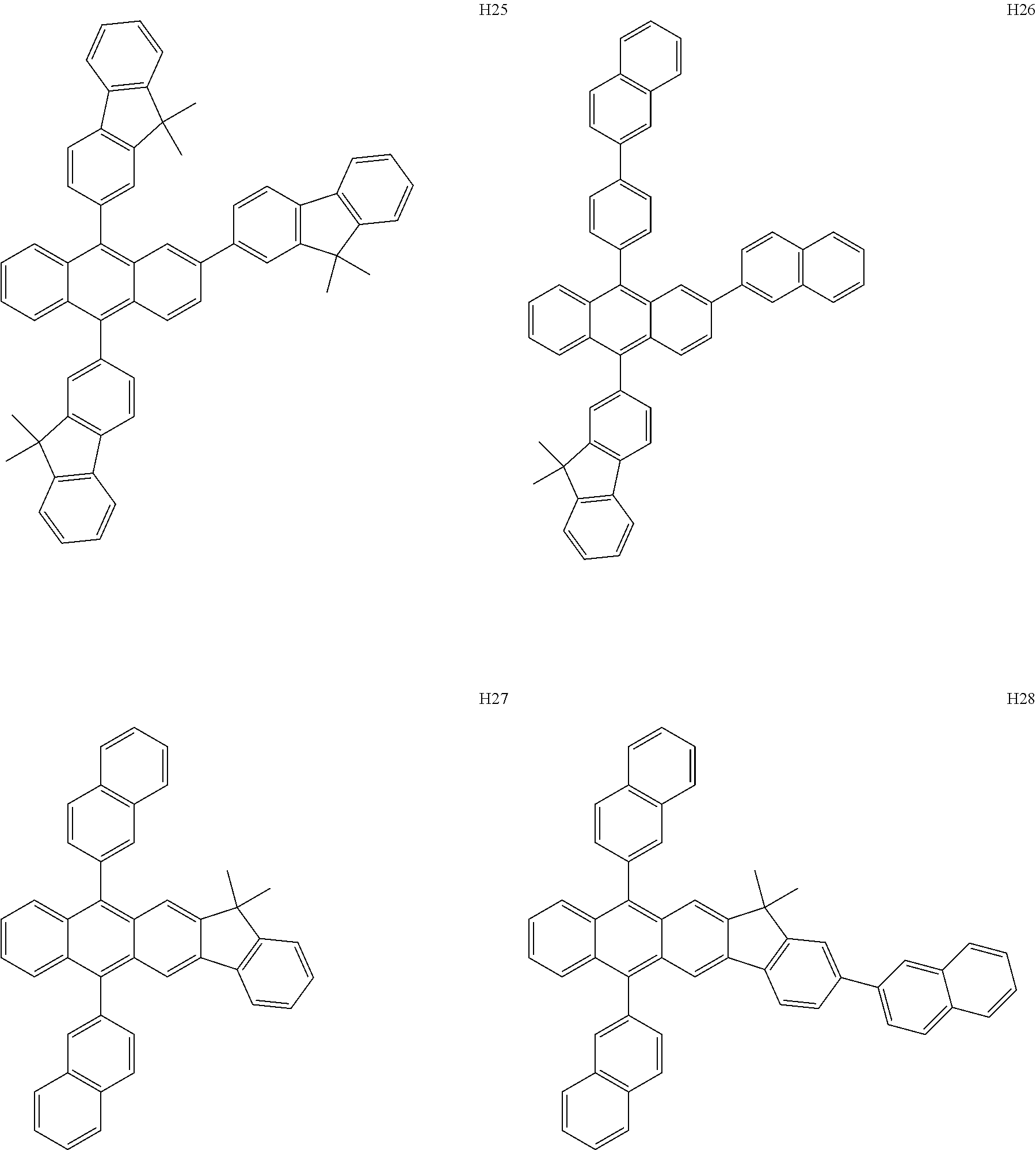


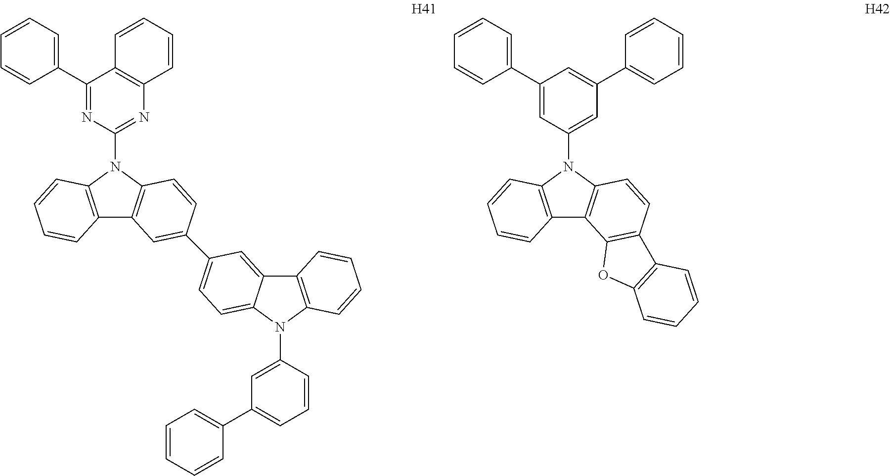


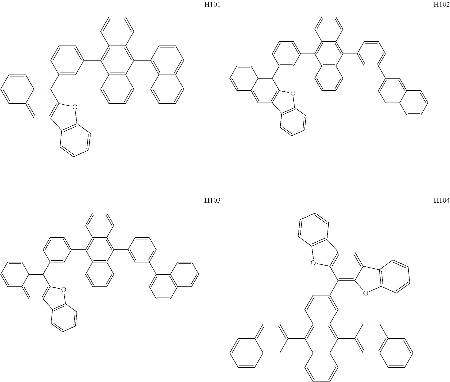
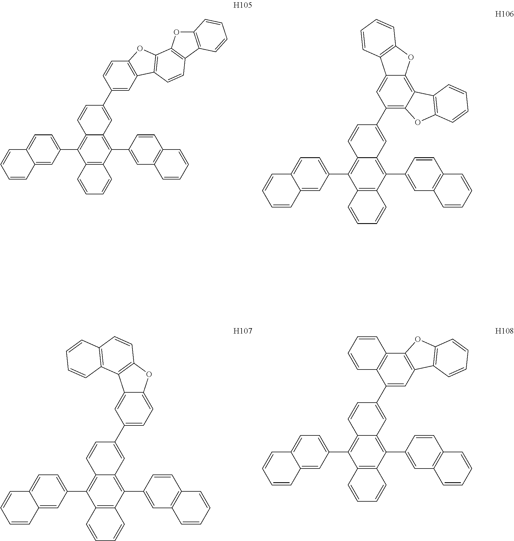

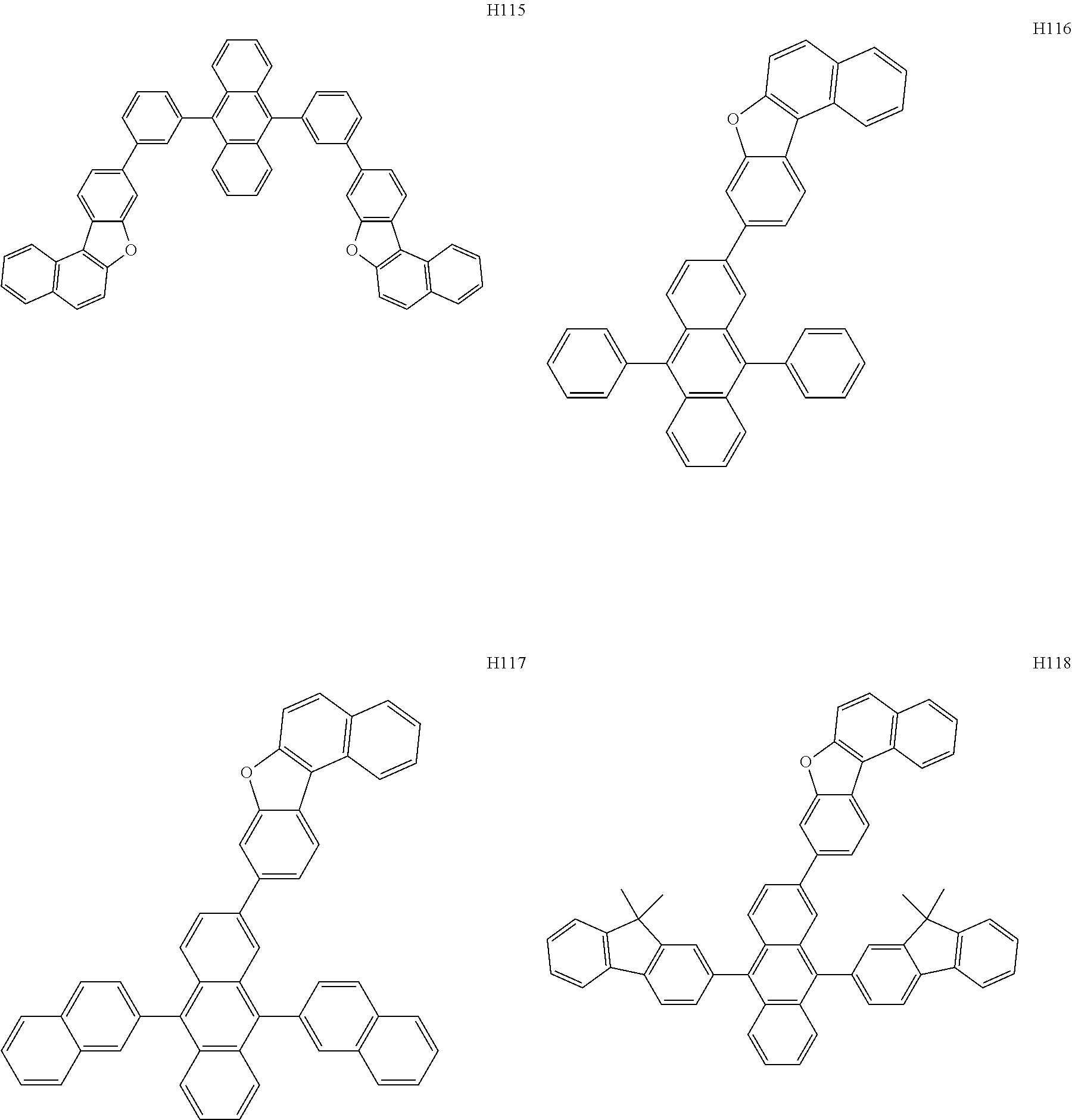
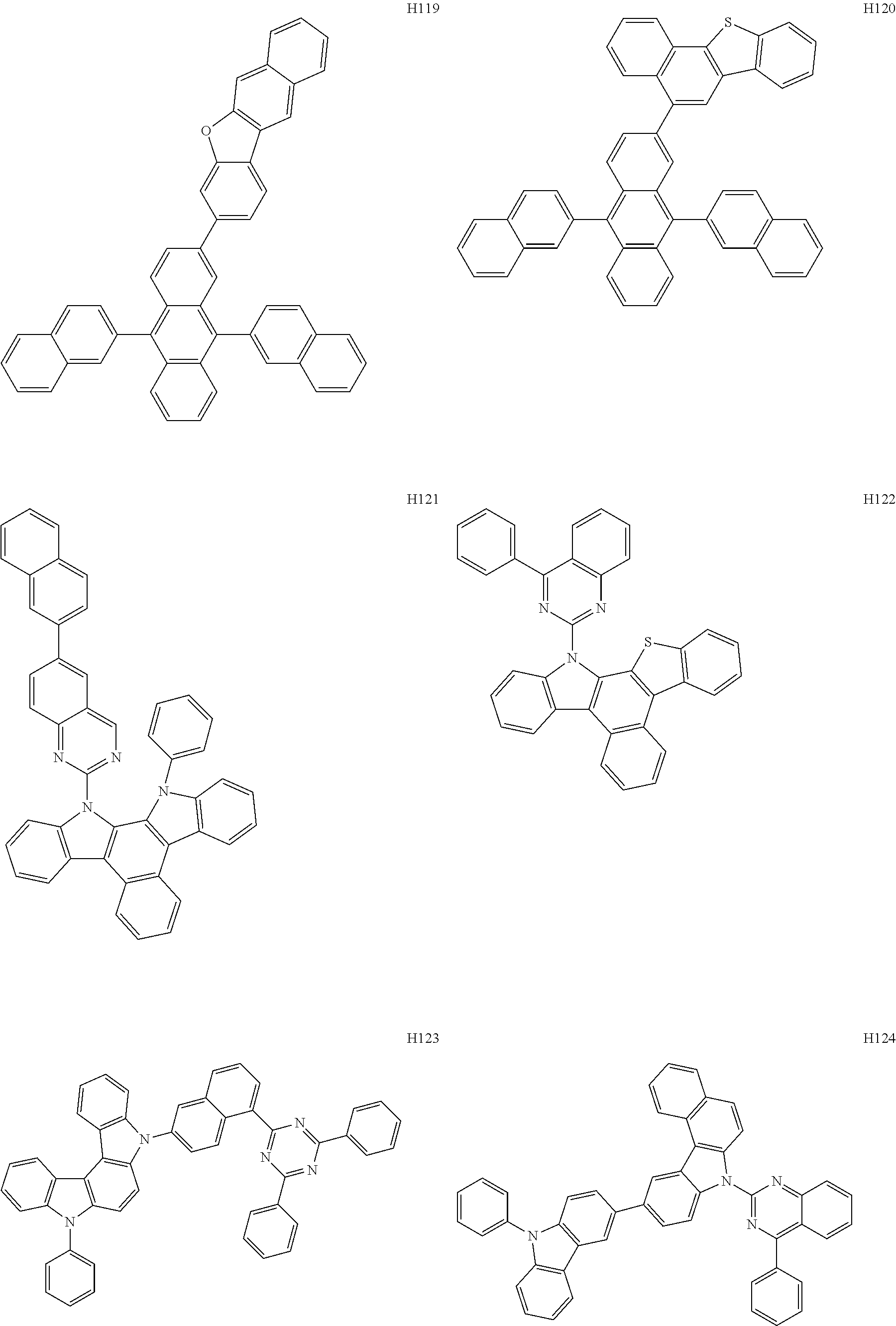


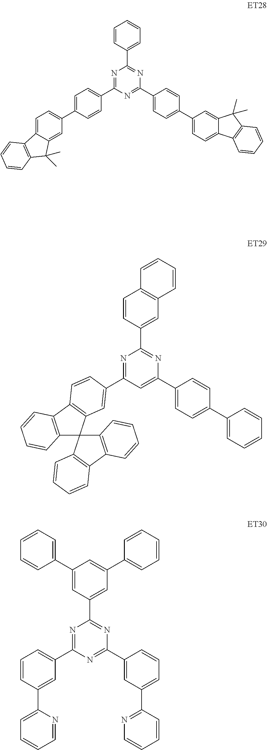


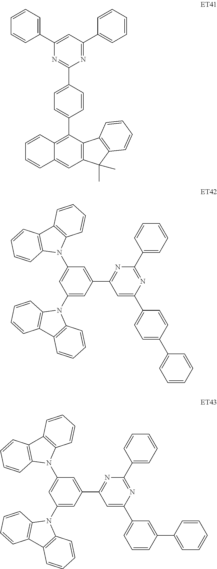


D00000

D00001
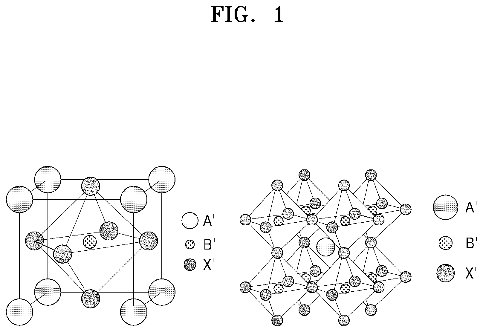
D00002
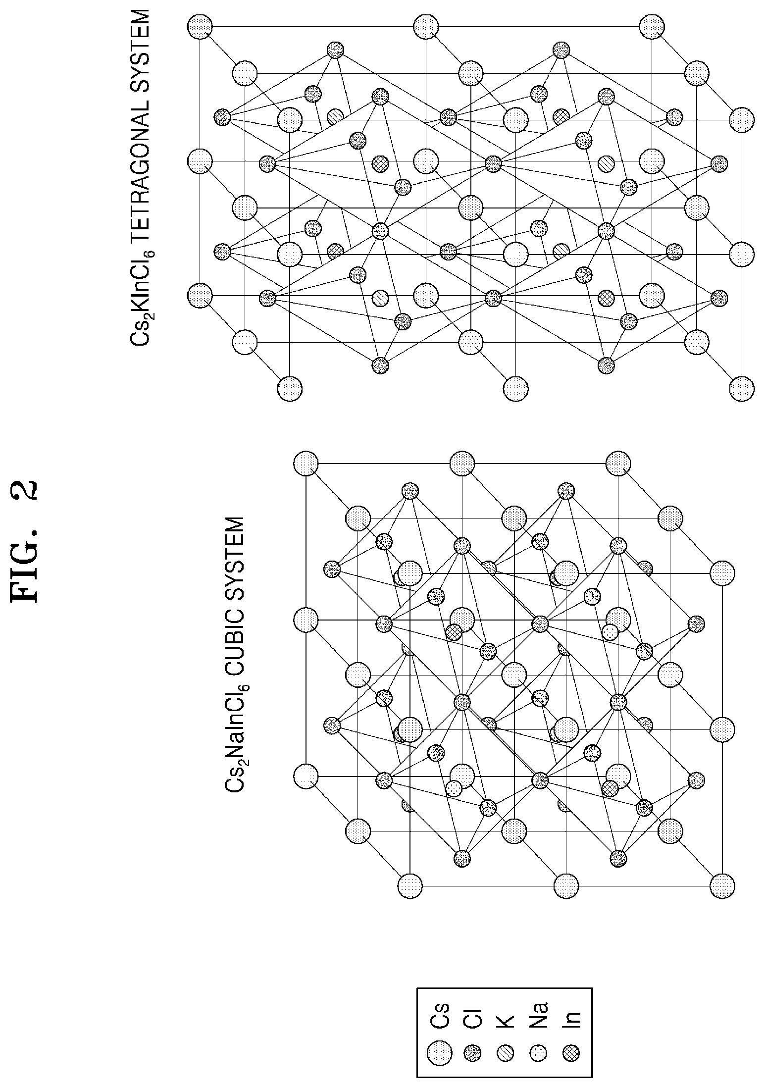
D00003

D00004

D00005

D00006
XML
uspto.report is an independent third-party trademark research tool that is not affiliated, endorsed, or sponsored by the United States Patent and Trademark Office (USPTO) or any other governmental organization. The information provided by uspto.report is based on publicly available data at the time of writing and is intended for informational purposes only.
While we strive to provide accurate and up-to-date information, we do not guarantee the accuracy, completeness, reliability, or suitability of the information displayed on this site. The use of this site is at your own risk. Any reliance you place on such information is therefore strictly at your own risk.
All official trademark data, including owner information, should be verified by visiting the official USPTO website at www.uspto.gov. This site is not intended to replace professional legal advice and should not be used as a substitute for consulting with a legal professional who is knowledgeable about trademark law.