Image Sensing Device
Yen; Shih-Chieh
U.S. patent application number 17/566444 was filed with the patent office on 2022-04-21 for image sensing device. This patent application is currently assigned to GUANGZHOU LUXVISIONS INNOVATION TECHNOLOGY LIMITED. The applicant listed for this patent is GUANGZHOU LUXVISIONS INNOVATION TECHNOLOGY LIMITED. Invention is credited to Shih-Chieh Yen.
| Application Number | 20220121016 17/566444 |
| Document ID | / |
| Family ID | |
| Filed Date | 2022-04-21 |


View All Diagrams
| United States Patent Application | 20220121016 |
| Kind Code | A1 |
| Yen; Shih-Chieh | April 21, 2022 |
IMAGE SENSING DEVICE
Abstract
An image sensing device includes a first light path changing element, a second light path changing element, and a plane lens. The first light path changing element includes a first light-incident side and a first light-emergent side, where the first light-incident side faces an image-capturing direction, the first light-emergent side faces a zoom optical axis, and there is an angle between the first light-incident side and the first light-emergent side. The second light path changing element includes a second light-incident side and a second light-emergent side, where the second light-incident side faces the zoom optical axis, the second light-emergent side faces an image-forming direction. An angle is between the second light-incident side and the second light-emergent side. An image-capturing light path passes through the first light-incident side, the first light-emergent side, the second light-incident side, and the second light-emergent side. The plane lens is disposed on the image-capturing light path.
| Inventors: | Yen; Shih-Chieh; (Guangzhou, CN) | ||||||||||
| Applicant: |
|
||||||||||
|---|---|---|---|---|---|---|---|---|---|---|---|
| Assignee: | GUANGZHOU LUXVISIONS INNOVATION
TECHNOLOGY LIMITED Guangzhou CN |
||||||||||
| Appl. No.: | 17/566444 | ||||||||||
| Filed: | December 30, 2021 |
Related U.S. Patent Documents
| Application Number | Filing Date | Patent Number | ||
|---|---|---|---|---|
| 63143158 | Jan 29, 2021 | |||
| International Class: | G02B 13/00 20060101 G02B013/00; G03B 13/34 20060101 G03B013/34; G02B 27/64 20060101 G02B027/64; G03B 5/00 20060101 G03B005/00; G02B 15/14 20060101 G02B015/14; H04N 5/232 20060101 H04N005/232 |
Foreign Application Data
| Date | Code | Application Number |
|---|---|---|
| Dec 8, 2021 | CN | 202111492317.8 |
Claims
1. An image sensing device, comprising: a first light path changing element, comprising a first light-incident side and a first light-emergent side, wherein the first light-incident side faces an image-capturing direction, the first light-emergent side faces a zoom optical axis, and there is a first angle between the first light-incident side and the first light-emergent side; a second light path changing element, comprising a second light-incident side and a second light-emergent side, wherein the second light-incident side faces the zoom optical axis, so that the first light-emergent side and the second light-incident side are disposed opposite to each other along the zoom optical axis; the second light-emergent side faces an image-forming direction, and there is a second angle between the second light-incident side and the second light-emergent side; and an image-capturing light path is formed between the first light path changing element and the second light path changing element, and sequentially passes through the first light-incident side, the first light-emergent side, the second light-incident side, and the second light-emergent side; and a plane lens, disposed on the image-capturing light path.
2. The image sensing device according to claim 1, wherein the first light path changing element is a first prism, comprising a first light-incident surface and a first light-emergent surface, wherein the first light-incident side is the first light-incident surface of the first prism, and the first light-emergent side is the first light-emergent surface of the first prism; and/or the second light path changing element is a second prism, comprising a second light-incident surface and a second light-emergent surface, wherein the second light-incident side is the second light-incident surface of the second prism, and the second light-emergent side is the second light-emergent surface of the second prism.
3. The image sensing device according to claim 1, wherein the first light path changing element is a first reflector, which is disposed at an angle to the image-capturing direction and is disposed at an angle to the zoom optical axis; and/or the second light path changing element is a second reflector, which is disposed at an angle to the image-forming direction and is disposed at an angle to the zoom optical axis.
4. The image sensing device according to claim 1, wherein the plane lens is a metalens or a multi-level diffractive lens (MDL).
5. The image sensing device according to claim 4, wherein there are a plurality of plane lenses, one of the plurality of plane lenses is a metalens, and another one of the plurality of plane lenses is an MDL.
6. The image sensing device according to claim 1, wherein the first light path changing element comprises a first light-incident surface and a first light-emergent surface, and the plane lens is disposed corresponding to the first light-incident surface.
7. The image sensing device according to claim 6, further comprising: a lens group, located between the first light path changing element and the second light path changing element.
8. The image sensing device according to claim 1, wherein the plane lens is located between the first light path changing element and the second light path changing element, and the zoom optical axis passes through the plane lens.
9. The image sensing device according to claim 8, further comprising: a focusing mechanism, connected to the plane lens, and configured to drive the plane lens to move along the zoom optical axis.
10. The image sensing device according to claim 8, further comprising: a lens group, located between the first light path changing element and the second light path changing element.
11. The image sensing device according to claim 10, wherein the plane lens is located between a plurality of lenses of the lens group.
12. The image sensing device according to claim 1, further comprising: an image sensor, disposed corresponding to the second light-emergent side.
13. The image sensing device according to claim 12, further comprising: a vibration compensation element, wherein the first light path changing element, the second light path changing element, and the plane lens together form a focal point, and the vibration compensation element is configured to adjust a landing point of the focal point on the image sensor.
14. The image sensing device according to claim 13, wherein the vibration compensation element is a vibration compensation lens group, is disposed on the image-capturing light path, and is configured to deflect light to adjust the landing point of the focal point on the image sensor.
15. The image sensing device according to claim 13, wherein the vibration compensation element is a multi-axis rotary actuator, is connected to the second light path changing element, and is configured to rotate the second light path changing element in a multi-axial direction.
16. The image sensing device according to claim 13, wherein the vibration compensation element is a multi-axis translational actuator, is connected to the image sensor, and is configured to translate the image sensor in a multi-axial direction.
Description
CROSS-REFERENCES TO RELATED APPLICATIONS
[0001] This application claims the benefit of U.S. provisional application Ser. No. 63/143,158, filed on Jan. 29, 2021 and claims the priority of Patent Application No. 202111492317.8 filed in China, P.R.C. on Dec. 8, 2021. The entirety of the above-mentioned patent applications are hereby incorporated by references herein and made a part of the specification.
BACKGROUND
Technical Field
[0002] The present invention relates to an image sensing device, and in particular, to an image sensing device for high magnification zooming.
Related Art
[0003] Existing thin electronic devices such as smartphones have a small thickness and limited internal space. When an electronic device needs to be equipped with a high-magnification camera, the optical lens group needs to adopt a periscope design, in which the optical lens group "lies transversely" inside the camera body, to configure an optical lens group with a long light path in the limited internal space. In addition, to increase the magnification, the optical lens group needs to be equipped with a zoom lens group including a plurality of zoom lenses, and a distance between the lenses of the optical lens group is extended as much as possible.
[0004] One or more lenses in the zoom lens group need to be moved with a long stroke, to achieve focusing and zooming. To achieve a long-stroke movement, a drive motor also needs to have a sufficient stroke to move the one or more lenses. In addition, to achieve a precise long-stroke movement, a guide rod and a lead screw configured to guide the one or more lenses also need to have high machining precision and high assembly precision, resulting in a high production difficulty.
SUMMARY
[0005] In view of this, the inventor puts forward an image sensing device. The image sensing device includes a first light path changing element, a second light path changing element, and a plane lens. The first light path changing element includes a first light-incident side and a first light-emergent side, where the first light-incident side faces an image-capturing direction, the first light-emergent side faces a zoom optical axis, and there is a first angle between the first light-incident side and the first light-emergent side. The second light path changing element includes a second light-incident side and a second light-emergent side, where the second light-incident side faces the zoom optical axis, so that the first light-emergent side and the second light-incident side are disposed opposite to each other along the zoom optical axis; the second light-emergent side faces an image-forming direction, and there is a second angle between the second light-incident side and the second light-emergent side; and an image-capturing light path is formed between the first light path changing element and the second light path changing element, and sequentially passes through the first light-incident side, the first light-emergent side, the second light-incident side, and the second light-emergent side. The plane lens is disposed on the image-capturing light path.
BRIEF DESCRIPTION OF THE DRAWINGS
[0006] FIG. 1 is a schematic diagram of an image sensing device disclosed in a first embodiment of the present disclosure.
[0007] FIG. 2 is a schematic diagram of an image sensing device disclosed in a second embodiment of the present disclosure.
[0008] FIG. 3A is a schematic diagram of an image sensing device disclosed in a third embodiment of the present disclosure.
[0009] FIG. 3B is an astigmatic field curvature diagram of the image sensing device disclosed in the third embodiment of the present disclosure.
[0010] FIG. 3C is a distortion diagram of the image sensing device disclosed in the third embodiment of the present disclosure.
[0011] FIG. 4A is a schematic diagram of an image sensing device disclosed in a fourth embodiment of the present disclosure.
[0012] FIG. 4B is an astigmatic field curvature diagram of the image sensing device disclosed in the fourth embodiment of the present disclosure.
[0013] FIG. 4C is a distortion diagram of the image sensing device disclosed in the fourth embodiment of the present disclosure.
[0014] FIG. 5A is a schematic diagram of an image sensing device disclosed in a fifth embodiment of the present disclosure.
[0015] FIG. 5B is an astigmatic field curvature diagram of the image sensing device disclosed in the fifth embodiment of the present disclosure.
[0016] FIG. 5C is a distortion diagram of the image sensing device disclosed in the fifth embodiment of the present disclosure.
[0017] FIG. 6A is a schematic diagram of an image sensing device disclosed in a sixth embodiment of the present disclosure.
[0018] FIG. 6B is an astigmatic field curvature diagram of the image sensing device disclosed in the sixth embodiment of the present disclosure.
[0019] FIG. 6C is a distortion diagram of the image sensing device disclosed in the sixth embodiment of the present disclosure.
[0020] FIG. 7A is a schematic diagram of an image sensing device disclosed in a seventh embodiment of the present disclosure.
[0021] FIG. 7B is an astigmatic field curvature diagram of the image sensing device disclosed in the seventh embodiment of the present disclosure.
[0022] FIG. 7C is a distortion diagram of the image sensing device disclosed in the seventh embodiment of the present disclosure.
[0023] FIG. 8 is a schematic diagram of an image sensing device disclosed in an eighth embodiment of the present disclosure.
[0024] FIG. 9 is a schematic diagram of an image sensing device disclosed in a ninth embodiment of the present disclosure.
DETAILED DESCRIPTION
[0025] FIG. 1 is a schematic diagram of an image sensing device disclosed in a first embodiment of the present disclosure. Referring to FIG. 1, the image sensing device 100 includes a first light path changing element 110, a second light path changing element 120, and a plane lens 130. The image sensing device 100 is applicable to an electronic device, for example, but not limited to a mobile phone, a tablet computer, or a notebook computer. In the first embodiment, the image sensing device 100 further includes an image sensor 140. The image sensor 140 may be a photosensitive element of the electronic device, such as a charge-coupled device (CCD) or a complementary metal-oxide-semiconductor active pixel sensor (CMOS active pixel sensor), to capture an image according to a photosensitive state and perform encoding to convert the image into a corresponding electronic signal. In some embodiments, the first light path changing element 110, the second light path changing element 120, and the plane lens 130 together form an optical assembly, which cooperates with the independently configured image sensor 140.
[0026] The first light path changing element 110 includes a first light-incident side 111 and a first light-emergent side 112. The first light-incident side 111 faces an image-capturing direction C, and the first light-emergent side 112 faces a zoom optical axis L. There is a first angle between the first light-incident side 111 and the first light-emergent side 112. The first angle may be a 90-degree angle, but other angles are not excluded. In an embodiment, the first light path changing element 110 is a first prism, and the first light-incident side 111 and the first light-emergent side 112 are a first light-incident surface and a first light-emergent surface of the first prism respectively. In a second embodiment, as shown in FIG. 2, the first light path changing element 110 is a first reflector, and is disposed at an angle to each of the image-capturing direction C and the zoom optical axis L, for example, but not limited to a 45-degree angle.
[0027] The second light path changing element 120 includes a second light-incident side 121 and a second light-emergent side 122. The second light-incident side 121 faces the zoom optical axis L, so that the first light-emergent side 112 of the first light path changing element 110 and the second light-incident side 121 of the second light path changing element 120 are disposed opposite to each other along the zoom optical axis L. The second light-emergent side 122 faces an image-forming direction I. There is a second angle between the second light-incident side 121 and the second light-emergent side 122. The second angle may be a 90-degree angle, but other angles are not excluded. In an embodiment, the second light path changing element 120 is a second prism, and the second light-incident side 121 and the second light-emergent side 122 are a second light-incident surface and a second light-emergent surface of the second prism respectively. In the second embodiment, as shown in FIG. 2, the second light path changing element 120 is a second reflector, and is disposed at an angle to each of the image-forming direction I and the zoom optical axis L, for example, but not limited to a 45-degree angle. Therefore, the first light path changing element 110 or the second light path changing element 120 may be a prism, a reflector, or a combination thereof. For example, the reflector is attached to an outer surface of a reflecting surface of the prism, or a reflecting surface of the prism is coated with a reflecting film.
[0028] An image-capturing light path is formed between the first light path changing element 110 and the second light path changing element 120, and sequentially passes through the first light-incident side 111, the first light-emergent side 112, the second light-incident side 121, and the second light-emergent side 122.
[0029] The plane lens 130 may be a metalens or a multi-level diffractive lens (MDL). The plane lens 130 is disposed on the image-capturing light path. In some embodiments, the plane lens 130 is located between the first light path changing element 110 and the second light path changing element 120, and the zoom optical axis L passes through the plane lens 130.
[0030] As shown in FIG. 1, the image sensor 140 is disposed corresponding to the second light-emergent side 122 of the second light path changing element 120. That is, the image-forming direction I faces the image sensor 140. Light received by the first light-incident side 111 of the first light path changing element 110 in the image-capturing direction C passes through the first light-emergent side 112, and is focused through the plane lens 130, and the focused light is imaged on the image sensor 140 through the second light-incident side 121 and the second light-emergent side 122.
[0031] As shown in FIG. 1 and FIG. 2, the plane lens 130 has a characteristic of a short focal length, and may complete high magnification zooming within a short light path. Therefore, a distance between the first light path changing element 110 and the second light path changing element 120 can be effectively shortened. In some embodiments, the image sensing device 100 further includes a focusing mechanism 150, connected to the plane lens 130, and configured to drive the plane lens 130 to move along the zoom optical axis L to perform focusing and zooming. The focusing mechanism 150 may be a voice coil motor (VCM), a shape memory alloy (SMA) motor, a piezo motor, or a combination of two or more thereof.
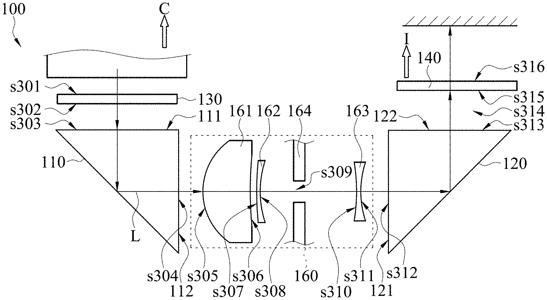
[0032] FIG. 3A is a schematic diagram of an image sensing device disclosed in a third embodiment of the present disclosure. Referring to FIG. 3A, the image sensing device 100 includes a first light path changing element 110, a second light path changing element 120, a plane lens 130, and an image sensor 140. In the third embodiment, configurations of the first light path changing element 110, the second light path changing element 120, and the image sensor 140 are substantially the same as those in the first embodiment. In the third embodiment, the plane lens 130 is also disposed on the image-capturing light path, and the plane lens 130 is disposed corresponding to a first light-incident side 111 of the first light path changing element 110. That is, the plane lens 130 is located in an image-capturing direction, and first performs high magnification zooming on incident light, and the first light-incident side 111 of the first light path changing element 110 then receives zoomed and refracted light.
[0033] As shown in FIG. 3A, the image sensing device 100 in the third embodiment further includes a lens group 160, including a plurality of lenses, such as lenses 161, 162, and 163. The lens group 160 is located between the first light path changing element 110 and the second light path changing element 120, and the lens group 160 is located on the zoom optical axis L. In an embodiment, the lens group 160 includes a focusing mechanism (not shown in the figure), configured to drive one or more lenses to move along the zoom optical axis L to perform focusing and zooming. Because a function of zooming a magnification is mainly achieved by the plane lens 130, the one or more lenses of the lens group 160 only need to be shifted within a short stroke, thereby effectively reducing a production difficulty, and shortening a length of the image sensing device 100 on the zoom optical axis L. The lenses 161, 162, and 163 of the lens group 160 may be aspheric lenses made of quartz or plastic. In the third embodiment, the lens 161 and the lens 162 are convex-concave lenses, and the lens 163 is a biconcave lens. Table 1 is a lens parameter table of the image sensing device disclosed in the third embodiment of the present disclosure (attached as an appendix at the end of this specification), referring to FIG. 3A supplemented with Table 1. Rows in Table 1 are arranged in an order in which light is projected onto the image sensor 140 after entering the image sensing device 100. For example, light is incident from a surface s301 of the plane lens 130, and is then emergent from a surface s302 of the plane lens 130, and an optical axis path length by which the light passes in the plane lens 130 is 0.5 mm; next, light is incident from the surface s302 of the plane lens 130 to a surface s303 of the first light path changing element 110, and an optical axis path length by which the light passes in a space gap is 0.35 mm; and then, light is incident from the surface s303 of the first light path changing element 110, and is then incident to a surface s304 of the first light path changing element 110 after being reflected in the first light path changing element 110. An optical axis path length by which the light passes in the first light path changing element 110 is 5.8 mm (2.9 mm before reflection+2.9 mm after reflection), and the rest may be deduced by analogy. In the third embodiment, the surface s303 and the surface s304 of the first light path changing element 110 are planes, and therefore, curvature radiuses are infinity; and a surface s305 and a surface s306 of the lens 161 are curved surfaces, and curvature radiuses are sequentially 2.922 mm and 455.122 mm.
[0034] According to the following sag function (Formula 1), an aspheric lens in the image sensing device 100 is described:
Z .function. ( s ) = Cs 2 1 + 1 - ( 1 + k ) .times. C 2 .times. s 2 + A 4 .times. s 4 + A 6 .times. s 6 + A 8 .times. s 8 + A 10 .times. s 10 + ( Formula .times. .times. 1 ) ##EQU00001##
[0035] where Z is a surface profile of a surface parallel to the optical axis; s is a radial distance from the optical axis; C is a curvature; k is a conic constant; and A.sub.4, A.sub.6, A.sub.8, and A.sub.10 are 4.sup.th-order, 6.sup.th-order, 8.sup.th-order, and 10.sup.th-order aspheric coefficients. Table 2 is a coefficient table of an aspheric formula of the image sensing device disclosed in the third embodiment of the present disclosure, referring to Table 1 and Table 2 together supplemented with the foregoing Formula 1. The surface s305 of the lens 161 is used as an example. A profile of the surface s305 is described by using Formula 1, where a conic constant k is 0, 4.sup.th-order, 6.sup.th-order, 8.sup.th-order, and 10.sup.th-order aspheric coefficients are sequentially 5.08E-04, 8.14E-05, 4.17E-06, and -1.69E-07, and a curvature radius is 2.922 mm.
[0036] According to the following Binary 2 surface phase formula (Formula 2), the plane lens 130 in the image sensing device 100 is described:
.phi.=M.SIGMA..sub.i=1.sup.NA.sub.i.rho..sup.2i (Formula 2)
[0037] where .phi. is a phase; M is a diffraction order; N is a series of polynomial coefficients; and A.sub.i is a polynomial coefficient in a normalized radial aperture coordinate .rho..sup.2i, and .rho. is an element radius. Table 3 is a coefficient table of the Binary 2 surface phase formula of the plane lens disclosed in the third embodiment of the present disclosure, referring to Table 3 supplemented with the foregoing Formula 2. The surface s301 of the plane lens 130 is used as an example, and a surface phase change of the surface s305 is described by using Formula 2, where .rho..sup.2, .rho..sup.4, .rho..sup.6, and .rho..sup.8 are sequentially -2.75E+05, -4.17E+07, -5.04E+10, and -1.17E+13.
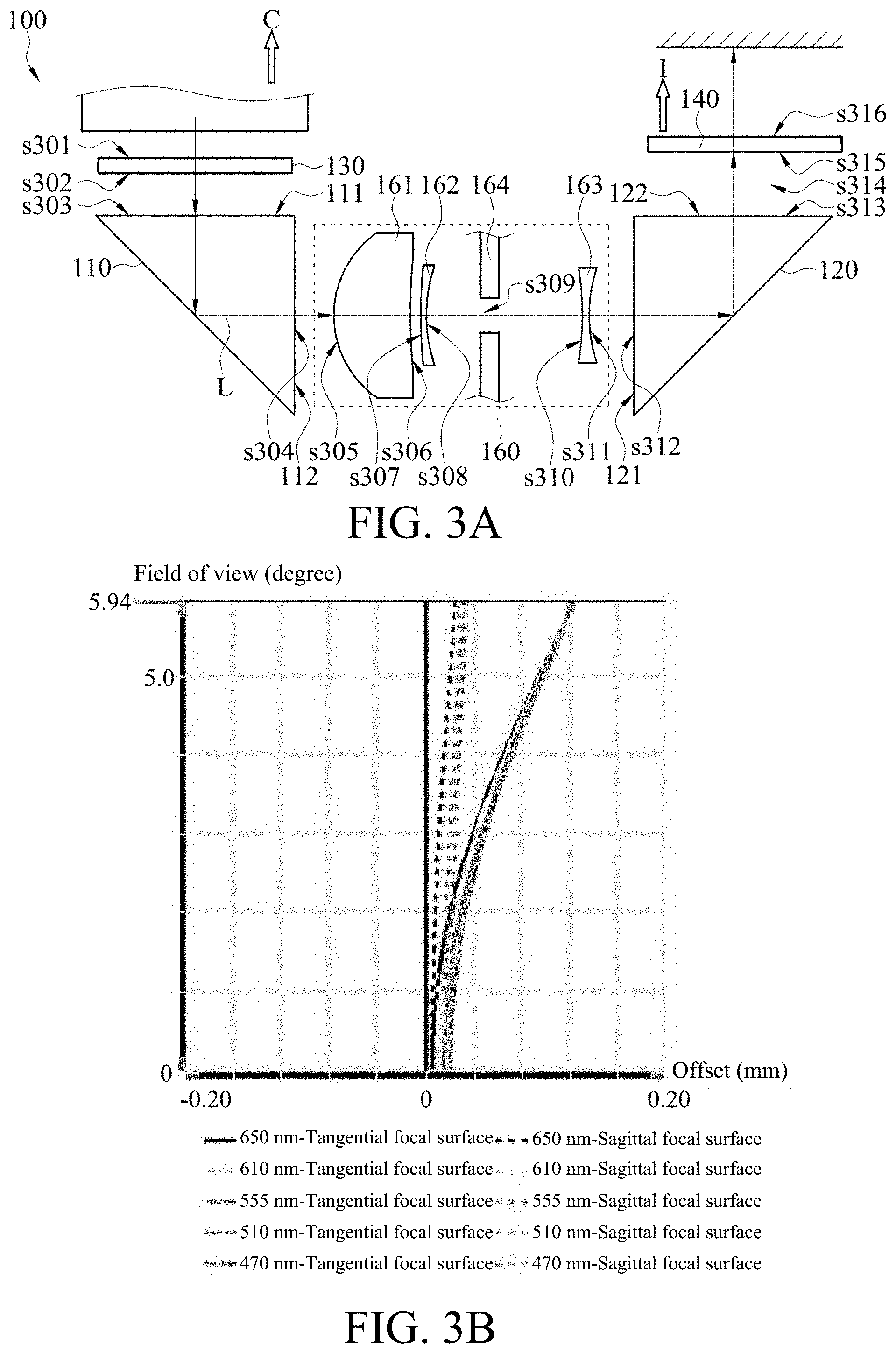
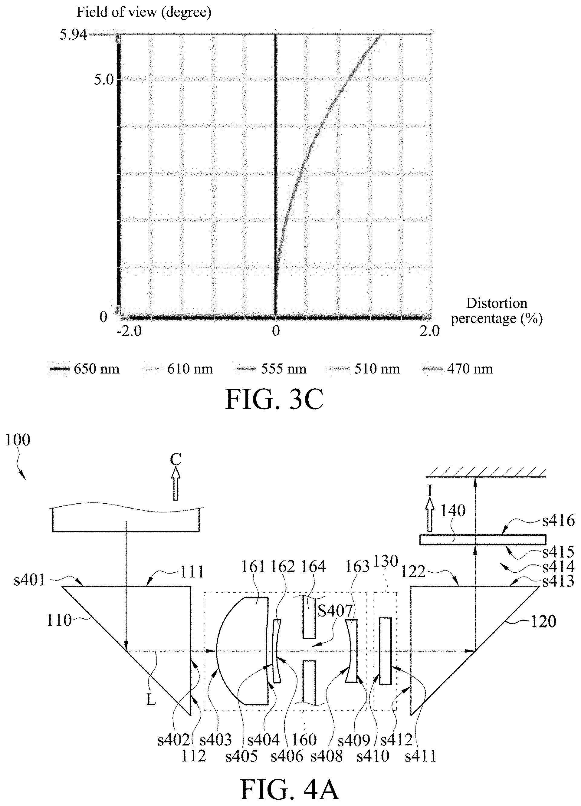
[0038] FIG. 3B and FIG. 3C are an astigmatic field curvature diagram and a distortion diagram of the image sensing device disclosed in the third embodiment of the present disclosure, referring to FIG. 3B and FIG. 3C together. A transverse axis in FIG. 3B is an offset between an imaging focus and a paraxial focal plane; and a longitudinal axis is a field of view of the imaging focus and the optical axis. FIG. 3B shows focus offsets of light with different wavelengths (650 nm, 610 nm, 555 nm, 510 nm, and 470 nm) on a tangential focal surface by using solid lines; and shows focus offsets of light with different wavelengths (650 nm, 610 nm, 555 nm, 510 nm, and 470 nm) on a sagittal focal surface by using dashed lines. A transverse axis in FIG. 3C is a distortion percentage; and a longitudinal axis is a field of view of the imaging focus and the optical axis. In this embodiment, a maximum field of view of imaging is 5.94 degrees, a tangential field curvature is 0.1094 mm, a sagittal field curvature is 0.0162 mm, and a maximum distortion is 1.3516%.
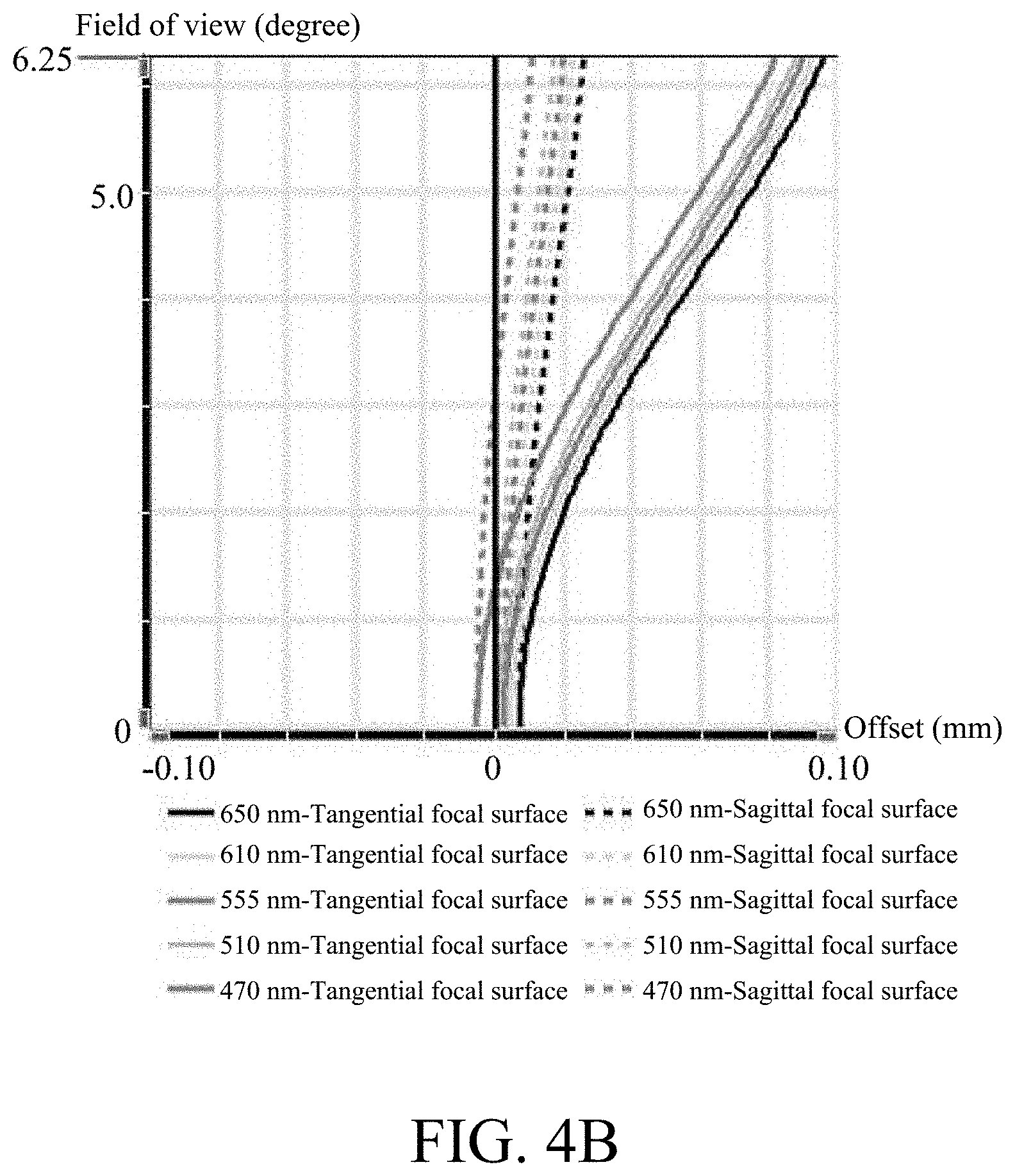
[0039] FIG. 4A is a schematic diagram of an image sensing device disclosed in a fourth embodiment of the present disclosure. Referring to FIG. 4A, the image sensing device 100 includes a first light path changing element 110, a second light path changing element 120, a plane lens 130, a lens group 160, and an image sensor 140. In the fourth embodiment, configurations of the first light path changing element 110, the second light path changing element 120, and the image sensor 140 are substantially the same as those in the first embodiment. In the fourth embodiment, both the plane lens 130 and the lens group 160 are located between the first light path changing element 110 and the second light path changing element 120, and both the plane lens 130 and the lens group 160 are located on the zoom optical axis L. For relative positions, the plane lens 130 may be disposed close to the first light path changing element 110, and the lens group 160 may be disposed close to the second light path changing element 120. Therefore, the plane lens 130 first performs high magnification zooming on light emergent from the first light-emergent side 112, and the lens group 160 then performs further focusing and zooming. Because a function of zooming a magnification is also achieved by the plane lens 130, one or more lenses of the lens group 160 only need to be shifted within a short stroke, thereby effectively reducing a production difficulty, and shortening a length of the image sensing device 100 on the zoom optical axis L. The foregoing relative position relationship is only an example, and the positions of the plane lens 130 and the lens group 160 may be arbitrarily changed. In the fourth embodiment, the lens 161 and the lens 162 are convex-concave lenses, and the lens 163 is a concave-convex lens. Table 4 is a lens parameter table of the image sensing device disclosed in the fourth embodiment of the present disclosure. Table 5 is a coefficient table of an aspheric formula of the image sensing device disclosed in the fourth embodiment of the present disclosure. Table 6 is a coefficient table of a Binary 2 surface phase formula of the plane lens disclosed in the fourth embodiment of the present disclosure. Refer to Table 4 to Table 6 together with the foregoing Formula 1 and Formula 2, to understand specifications of the image sensing device 100 in the fourth embodiment of the present disclosure.
[0040] FIG. 4B and FIG. 4C are an astigmatic field curvature diagram and a distortion diagram of the image sensing device disclosed in the fourth embodiment of the present disclosure. FIG. 4B shows focus offsets of light with different wavelengths on a tangential focal surface by using solid lines; and shows focus offsets of light with different wavelengths on a sagittal focal surface by using dashed lines. In this embodiment, a maximum field of view of imaging is 6.57 degrees, a tangential field curvature is 0.0734 mm, a sagittal field curvature is 0.0102 mm, and a maximum distortion is 0.5981%.
[0041] FIG. 5A is a schematic diagram of an image sensing device disclosed in a fifth embodiment of the present disclosure. Referring to FIG. 5A, in some embodiments, the plane lens 130 may alternatively be inserted between a plurality of lenses of lens groups 160. That is, the plane lens 130 is located between two lens groups 160, and each lens group 160 includes one or more lenses. For example, the plane lens 130 in the fifth embodiment is located between lenses 161 and 162 of a lens group 160 and a lens 163 of an other lens group 160. Alternatively, the plane lens 130 may be located between a lens 161 of a lens group 160 and lenses 162 and 163 of another lens group 160 (not shown in the figure). In the fifth embodiment, the lens 161 and the lens 162 are convex-concave lenses, and the lens 163 is a concave-convex lens. Table 7 is a lens parameter table of the image sensing device disclosed in the fifth embodiment of the present disclosure. Table 8 is a coefficient table of an aspheric formula of the image sensing device disclosed in the fifth embodiment of the present disclosure. Table 9 is a coefficient table of a Binary 2 surface phase formula of the plane lens disclosed in the fifth embodiment of the present disclosure. Refer to Table 7 to Table 9 together with the foregoing Formula 1 and Formula 2, to understand specifications of the image sensing device 100 in the fifth embodiment of the present disclosure.
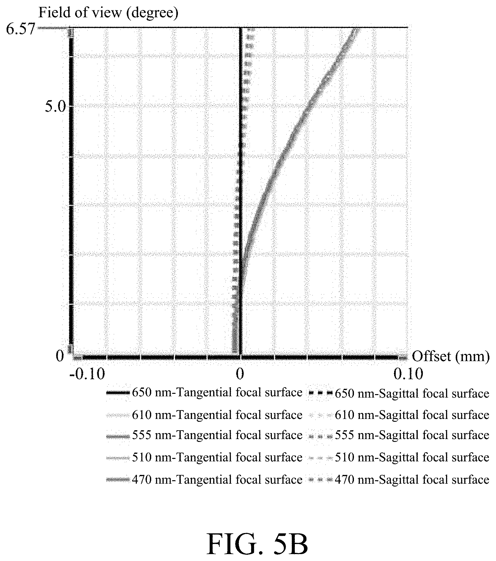
[0042] FIG. 5B and FIG. 5C are an astigmatic field curvature diagram and a distortion diagram of the image sensing device disclosed in the fifth embodiment of the present disclosure. FIG. 5B shows focus offsets of light with different wavelengths on a tangential focal surface by using solid lines; and shows focus offsets of light with different wavelengths on a sagittal focal surface by using dashed lines. In this embodiment, a maximum field of view of imaging is 6.57 degrees, a tangential field curvature is 0.0734 mm, a sagittal field curvature is 0.0102 mm, and a maximum distortion is 0.5981%.
[0043] FIG. 6A is a schematic diagram of an image sensing device disclosed in a sixth embodiment of the present disclosure. Referring to FIG. 6A, in some embodiments, the image sensing device 100 may include a plurality of plane lenses, for example, two plane lenses 130a and 130b. The two plane lenses 130a and 130b may be in different forms. For example, one plane lens 130a is a metalens, and an other plane lens 130b is an MDL. The plurality of plane lenses 130a and 130b may perform a plurality of times of zooming, to avoid an image edge distortion caused by performing a single time of zooming with an excessively high magnification. Similarly, one or more lenses of the lens group 160 only need to be shifted within a short stroke to perform additional focusing and zooming, to overcome a disadvantage of a lens group with a long stroke. In the sixth embodiment, the lens 161 and the lens 162 are convex-concave lenses, the lens 163 is a biconcave lens, and both the plane lens 130a and the plane lens 130b are metalenses. Table 10 is a lens parameter table of the image sensing device disclosed in the sixth embodiment of the present disclosure. Table 11 is a coefficient table of an aspheric formula of the image sensing device disclosed in the sixth embodiment of the present disclosure. Table 12 is a coefficient table of a Binary 2 surface phase formula of the plane lens disclosed in the sixth embodiment of the present disclosure. Refer to Table 10 to Table 12 together with the foregoing Formula 1 and Formula 2, to understand specifications of the image sensing device 100 in the sixth embodiment of the present disclosure.
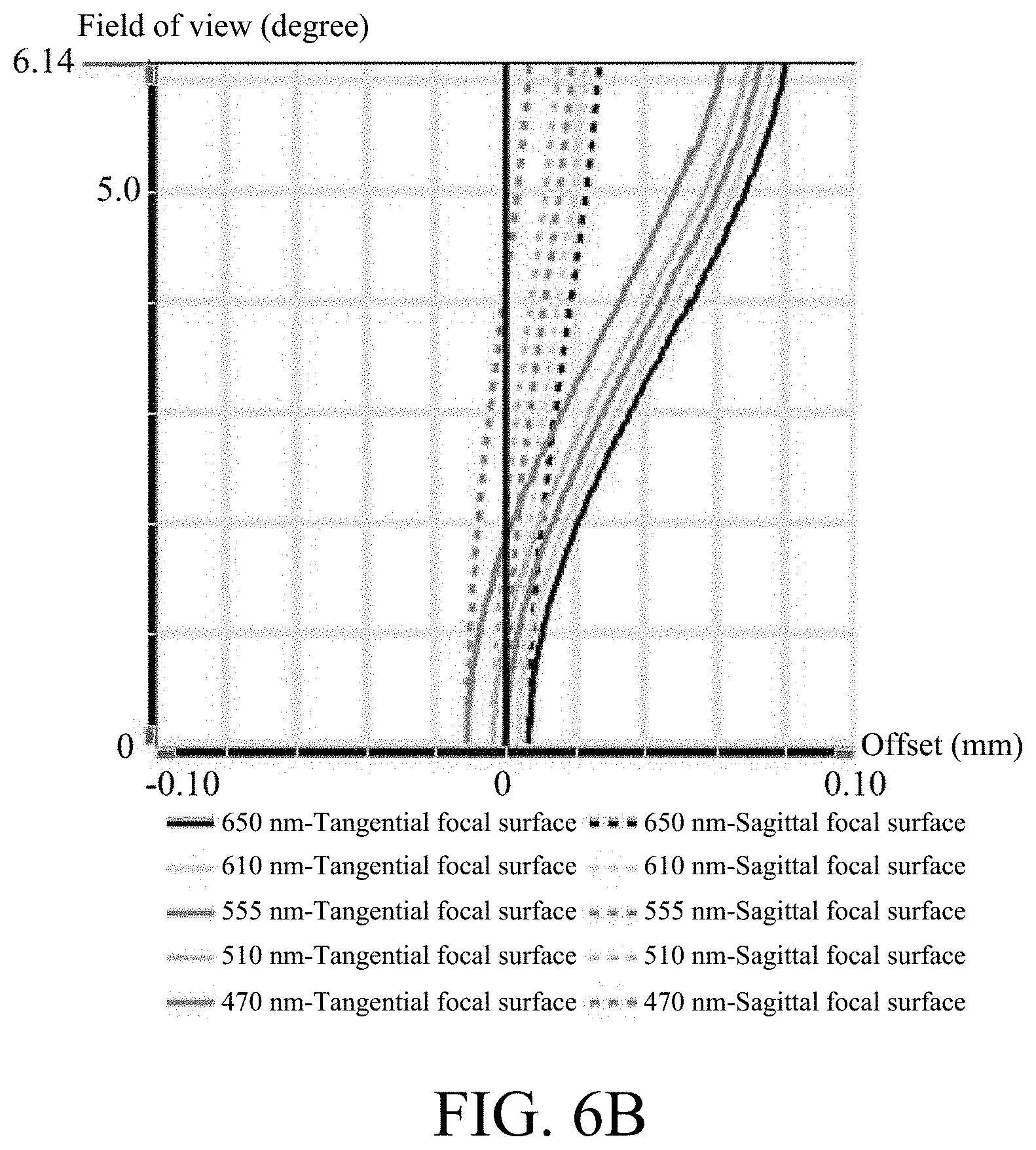
[0044] FIG. 6B and FIG. 6C are an astigmatic field curvature diagram and a distortion diagram of the image sensing device disclosed in the sixth embodiment of the present disclosure. FIG. 6B shows focus offsets of light with different wavelengths on a tangential focal surface by using solid lines; and shows focus offsets of light with different wavelengths on a sagittal focal surface by using dashed lines. In this embodiment, a maximum field of view of imaging is 6.14 degrees, a tangential field curvature is 0.0726 mm, a sagittal field curvature is 0.0190 mm, and a maximum distortion is 0.8914%.
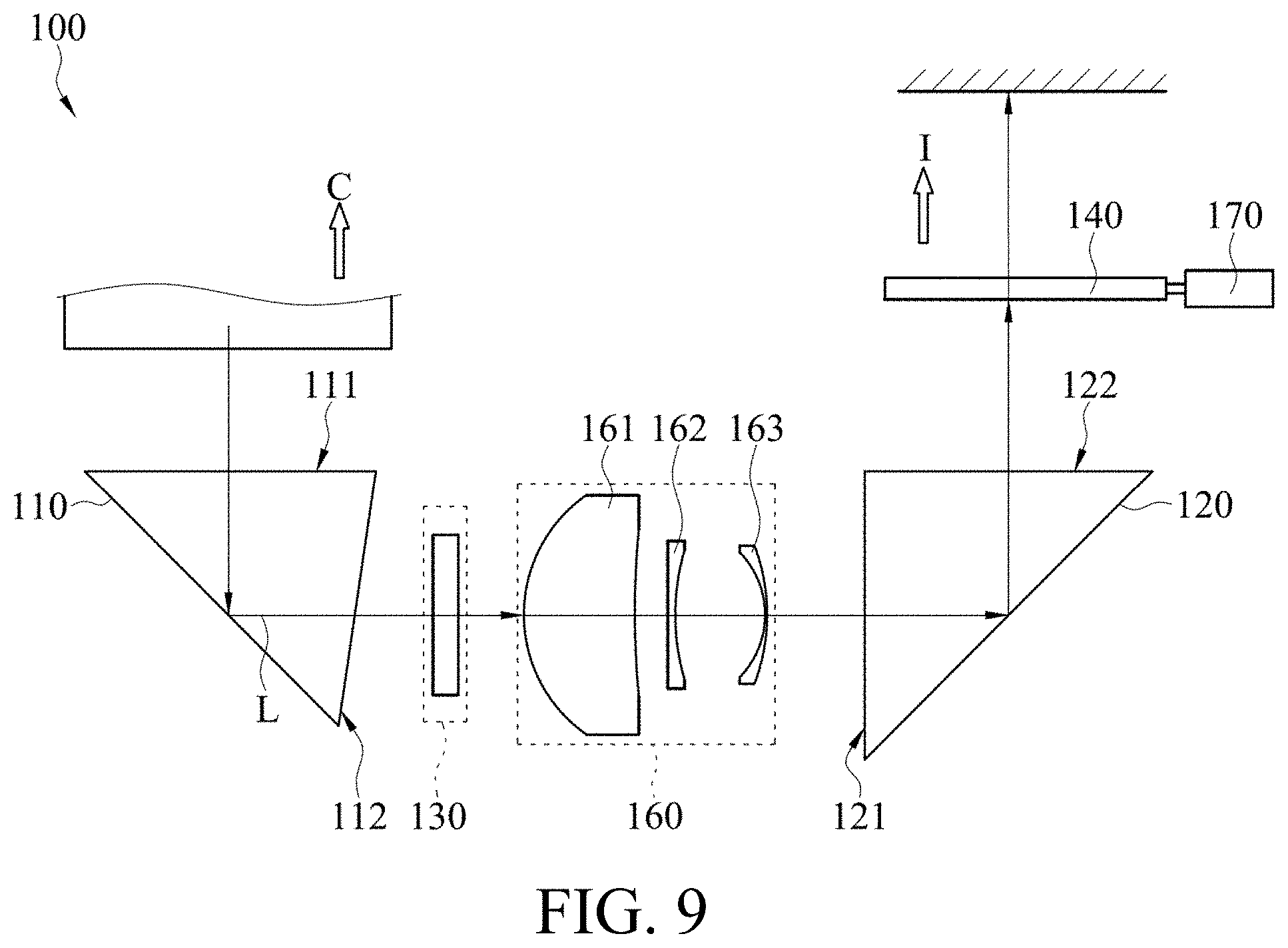
[0045] FIG. 7A, FIG. 8, and FIG. 9 show an image sensing device 100 according to some embodiments of the present invention. The image sensing device 100 further includes a vibration compensation element 170.
[0046] As shown in FIG. 7A, light is focused on the image sensor 140 through the first light path changing element 110, the vibration compensation element 170, the lens group 160, the plane lens 130, and the second light path changing element 120. The vibration compensation element 170 may be a vibration compensation lens group, configured to deflect light to adjust a landing point of a focal point on the image sensor 140 to achieve vibration compensation. The vibration compensation lens group may be located between the first light path changing element 110 and the second light path changing element 120, and corresponds to the first light-emergent side 112. In a seventh embodiment, the lens 161 and the lens 162 are convex-concave lenses, and the lens 163 is a concave-convex lens. Table 13 is a lens parameter table of an image sensing device disclosed in the seventh embodiment of the present disclosure. Table 14 is a coefficient table of an aspheric formula of the image sensing device disclosed in the seventh embodiment of the present disclosure. Table 15 is a coefficient table of a Binary 2 surface phase formula of the plane lens disclosed in the seventh embodiment of the present disclosure. Refer to Table 13 to Table 15 together with the foregoing Formula 1 and Formula 2, to understand specifications of the image sensing device 100 in the seventh embodiment of the present disclosure.
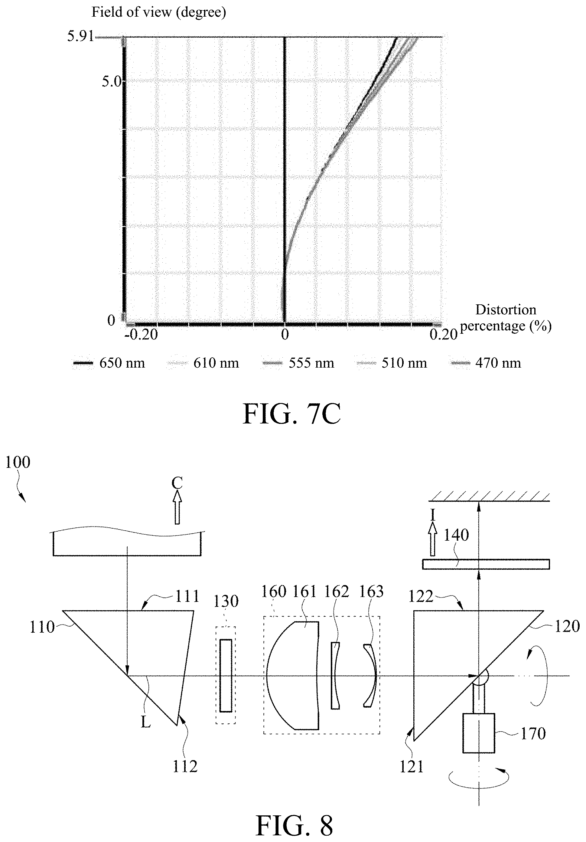
[0047] FIG. 7B and FIG. 7C are an astigmatic field curvature diagram and a distortion diagram of the image sensing device disclosed in the seventh embodiment of the present disclosure. FIG. 7B shows focus offsets of light with different wavelengths on a tangential focal surface by using solid lines; and shows focus offsets of light with different wavelengths on a sagittal focal surface by using dashed lines. In this embodiment, a maximum field of view of imaging is 5.91 degrees, a tangential field curvature is 0.0348 mm, a sagittal field curvature is 0.0310 mm, and a maximum distortion is 0.16%.
[0048] As shown in FIG. 8, the vibration compensation element 170 may be a multi-axis rotary actuator, is connected to the second light path changing element 120, and is configured to rotate the second light path changing element 120 in a multi-axial direction, to adjust a landing point of a focal point on the image sensor 140 to achieve vibration compensation.
[0049] As shown in FIG. 9, the vibration compensation element 170 may be a multi-axis translational actuator, is connected to the image sensor 140, and is configured to translate the image sensor 140 in a multi-axial direction, to adjust a landing point of a focal point on the image sensor 140 to achieve vibration compensation.
[0050] In summary, by using a characteristic of a short focal length of the plane lens 130 in the present disclosure, high magnification zooming may be completed within a short light path. Therefore, a distance between the first light path changing element 110 and the second light path changing element 120 may be effectively shortened; and the existing lens group 160 does not need to be configured to perform high magnification zooming, and one or more lenses of the lens group 160 only need to be shifted within a short stroke, thereby effectively reducing a production difficulty.
[0051] In the content recorded in this specification, when the terms "include", "comprise" or "have" are used, other elements, components, structures, areas, components, devices, systems, steps, connections, and the like may be additionally included unless otherwise stated, and other specifications shall not be excluded.
[0052] The features such as a proportional relationship, a structure, and a size shown in the figures of the present invention are only intended to describe the embodiments described in the present disclosure, to help a person of ordinary skill in the art to which the present invention belongs read and understand the present invention, are not intended to limit the scope of the claims of the present invention. In addition, any changes, modifications, or adjustments to the content recorded in the foregoing embodiments shall fall within the scope of the claims of the present invention, without affecting the inventive objectives and effects of the present disclosure.
TABLE-US-00001 TABLE 1 a lens parameter table of the image sensing device disclosed in the third embodiment of the present disclosure: Curvature Optical axis Refraction Dispersion Surface Object radius path length coefficient coefficient s301 Plane lens 130 -- 0.5 1.460 67.800 s302 -- -- 0.35 -- -- s303 First light path Infinity 5.800 1.85 23.79 changing element 110 s304 -- Infinity 0.700 -- -- s305 Lens 161 2.922 2.250 1.540 56.000 s306 -- 455.122 0.285 -- -- s307 Lens 162 32.932 0.150 1.640 22.400 s308 -- 5.133 0.245 -- -- s309 Aperture stop Infinity 2.377 -- -- 164 s310 Lens 163 -21.016 0.289 1.540 56.000 s311 -- 4.991 0.720 -- -- s312 Second light Infinity 5.800 1.85 23.79 path changing element 120 s313 -- Infinity 0.200 -- -- s314 -- Infinity 0.210 1.520 64.200 s315 -- Infinity 0.200 -- -- s316 Image sensor -- -- -- -- 140 Note: The curvature radius and the optical axis path length are measured in mm.
TABLE-US-00002 TABLE 2 a coefficient table of an aspheric formula of an image sensing device disclosed in a third embodiment of the present disclosure: Surface k A4 A6 A8 A10 s305 0 5.08E-04 8.14E-05 4.17E-06 -1.69E-07 s306 0 9.58E-03 -3.71E-03 8.17E-04 -6.13E-05 s307 0 -2.24E-03 -5.93E-04 2.23E-03 -3.59E-04 s308 0 -3.07E-03 4.98E-03 1.86E-03 1.16E-04 s310 0 -5.15E-02 3.32E-02 -2.44E-03 -4.33E-04 s311 0 -4.66E-02 3.22E-02 -4.47E-03 5.19E-04
TABLE-US-00003 TABLE 3 a coefficient table of a Binary 2 surface phase formula of a plane lens disclosed in the third embodiment of the present disclosure: Normalized Sur- curvature face radius .rho..sup.2 .rho..sup.4 .rho..sup.6 .rho..sup.8 s301 100 -2.75E+05 -4.17E+07 -5.04E+10 -1.17E+13 s302 100 3.23E+05 9.08E+07 -3.67E+09 3.06E+13
TABLE-US-00004 TABLE 4 a lens parameter table of an image sensing device disclosed in a fourth embodiment of the present disclosure: Curva- Sur- ture Optical axis Refraction Dispersion face Object radius path length coefficient coefficient s401 First light Infinity 5.800 1.85 23.79 path changing element 110 s402 -- Infinity 0.700 -- -- s403 Lens 161 2.922 2.250 1.540 56.000 s404 -- 455.122 0.285 -- -- s405 Lens 162 32.932 0.150 1.640 22.400 s406 -- 5.133 0.245 -- -- s407 Aperture Infinity 2.377 -- -- stop 164 s408 Lens 163 -4.473 0.292 1.540 56.000 s409 -- 263.852 0.100 -- -- s410 Plane Infinity 0.500 1.460 67.800 lens 130 s411 -- Infinity 0.200 -- -- s412 Second Infinity 5.800 1.85 23.79 light path changing element 120 s413 -- Infinity 0.200 -- -- s414 -- Infinity 0.210 1.520 64.200 s415 -- Infinity 0.200 -- -- s416 Image -- -- -- -- sensor 140 Note: The curvature radius and the optical axis path length are measured in mm.
TABLE-US-00005 TABLE 5 a coefficient table of an aspheric formula of the image sensing device disclosed in the fourth embodiment of the present disclosure: Surface k A4 A6 A8 A10 s403 0 6.02E-04 8.19E-05 9.34E-07 2.21E-06 s404 0 1.19E-02 -3.26E-03 8.86E-04 -1.22E-04 s405 0 -6.07E-04 -4.20E-04 2.05E-03 -4.58E-04 s406 0 -4.94E-03 4.35E-03 1.64E-03 -1.37E-04 s408 0 -5.92E-02 3.32E-02 -2.38E-03 -3.30E-04 s409 0 -4.97E-02 3.01E-02 -4.35E-03 5.14E-04
TABLE-US-00006 TABLE 6 a coefficient table of a Binary 2 surface phase formula of a plane lens disclosed in the fourth embodiment of the present disclosure: Normalized Sur- curvature face radius .rho..sup.2 .rho..sup.4 .rho..sup.6 .rho..sup.8 s410 5 7.46E+03 3.37E+04 5.97E+04 -2.12E+06 s411 5 -7.18E+03 -2.87E+04 -2.63E+05 3.63E+06
TABLE-US-00007 TABLE 7 a lens parameter table of the image sensing device disclosed in the fifth embodiment of the present disclosure: Refrac- Disper- Curva- Optical tion sion ture axis path coe- coe- Surface Object radius length fficient fficient s501 First light path Infinity 5.800 1.85 23.79 changing element 110 s502 -- Infinity 0.700 -- -- s503 Lens 161 2.979 2.250 1.540 56.000 s504 -- -566.158 0.285 -- -- s505 Lens 162 22.587 0.150 1.640 22.400 s506 -- 4.970 0.245 -- -- s507 Plane lens 130 Infinity 0.500 1.460 67.800 s508 -- Infinity 0.200 -- -- s509 Aperture stop Infinity 2.041 -- -- 164 s510 Lens 163 -3.434 0.234 1.540 56.000 s511 -- -15.586 0.245 -- -- s512 Second light Infinity 5.800 1.85 23.79 path changing element 120 s513 -- Infinity 0.200 -- -- s514 -- Infinity 0.210 1.520 64.200 s515 -- Infinity 0.200 -- -- s516 Image sensor -- -- -- 140 Note: The curvature radius and the optical axis path length are measured in mm.
TABLE-US-00008 TABLE 8 a coefficient table of an aspheric formula of the image sensing device disclosed in the fifth embodiment of the present disclosure: Surface k A4 A6 A8 A10 s503 0 4.12E-04 8.14E-05 -9.32E-06 2.73E-06 s504 0 1.17E-02 -3.23E-03 8.96E-04 -1.15E-04 s505 0 -3.16E-05 -3.20E-04 2.06E-03 -4.69E-04 s506 0 -5.18E-03 4.29E-03 1.52E-03 -1.90E-04 s510 0 -5.97E-02 3.21E-02 -2.98E-03 -4.54E-04 s511 0 -5.08E-02 2.98E-02 -4.59E-03 1.94E-04
TABLE-US-00009 TABLE 9 a coefficient table of a Binary 2 surface phase formula of a plane lens disclosed in the fifth embodiment of the present disclosure: Normalized Sur- curvature face radius .rho..sup.2 .rho..sup.4 .rho..sup.6 .rho..sup.8 s507 1.00E+02 4.30E+05 6.26E+07 -3.15E+12 -3.54E+15 s508 1.00E+02 -3.08E+05 3.41E+08 1.33E+12 2.65E+16
TABLE-US-00010 TABLE 10 a lens parameter table of an image sensing device disclosed in a sixth embodiment of the present disclosure: Optical Refrac- Disper- Curv- axis tion sion Sur- ature path coe- coe- face Object radius length fficient fficient s601 First light path Infinity 5.800 1.85 23.79 changing element 110 s602 -- Infinity 0.700 -- -- s603 Lens 161 2.949 2.250 1.540 56.000 s604 -- 175.377 0.285 -- -- s605 Lens 162 76.715 0.150 1.640 22.400 s606 -- 5.807 0.245 -- -- s607 Aperture stop Infinity 2.144 -- -- 164 s608 Lens 163 -6.347 0.284 1.540 56.000 s609 -- 20.401 0.100 -- -- s610 Plane lens Infinity 0.500 1.460 67.800 130a s611 -- Infinity 0.200 -- -- s612 Plane lens Infinity 0.500 1.460 67.800 130b s613 Infinity 0.200 -- -- s614 Second light Infinity 5.800 1.85 23.79 path changing element 120 s615 -- Infinity 0.200 -- -- s616 -- Infinity 0.210 1.520 64.200 s617 -- Infinity 0.200 -- -- s618 Image sensor -- -- -- -- 140 Note: The curvature radius and the optical axis path length are measured in mm.
TABLE-US-00011 TABLE 11 a coefficient table of an aspheric formula of the image sensing device disclosed in the sixth embodiment of the present disclosure: Surface k A4 A6 A8 A10 s607 0 8.06E-04 1.14E-04 -2.01E-07 3.22E-06 s608 0 1.26E-02 -3.49E-03 1.02E-03 -1.43E-04 s609 0 -5.74E-04 -9.24E-05 2.32E-03 -4.93E-04 s610 0 -6.16E-03 5.44E-03 1.45E-03 -7.96E-06 s612 0 -5.82E-02 3.11E-02 -1.26E-03 -5.17E-04 s613 0 -4.96E-02 3.08E-02 -4.39E-03 5.27E-04
TABLE-US-00012 TABLE 12 a coefficient table of a Binary 2 surface phase formula of a plane lens disclosed in the sixth embodiment of the present disclosure: Normalized Sur- curvature face radius .rho..sup.2 .rho..sup.4 .rho..sup.6 .rho..sup.8 s614 5 2.16E+03 -1.92E+03 5.83E+04 2.29E+05 s615 5 -3.47E+03 -2.81E+03 2.02E+04 -3.65E+05 s616 5 7.46E+03 3.37E+04 5.97E+04 -2.12E+06 s617 5 -5.85E+03 -2.60E+04 -2.53E+05 3.13E+06
TABLE-US-00013 TABLE 13 a lens parameter table of an image sensing device disclosed in a seventh embodiment of the present disclosure: Sur- Curvature Optical axis Refraction Dispersion face Object radius path length coefficient coefficient s701 First light path Infinity 5.800 1.7 59.05 changing element 110 s702 -- Infinity 0.700 -- -- s703 Vibration Infinity 0.600 1.7 59.05 compensation element 170a s704 -- Infinity 0.800 -- -- s705 Vibration Infinity 0.600 1.7 59.05 compensation element 170b s706 -- Infinity 0.800 -- -- s707 Lens 161 2.803 2.253 1.540 56.000 s708 -- -63.100 0.285 -- -- s709 Lens 162 36.683 0.150 1.640 22.400 s710 -- 4.545 0.245 -- -- s711 Aperture stop Infinity 2.507 -- -- 164 s712 Lens 163 -2.022 0.150 1.540 56.000 s713 -- -5.516 0.100 -- -- s714 Plane lens 130 Infinity 0.500 1.460 67.800 s715 -- Infinity 0.200 -- -- s716 Second light Infinity 5.800 1.85 23.79 path changing element 120 s717 -- Infinity 0.200 -- -- s718 -- Infinity 0.210 1.520 64.200 s719 -- Infinity 0.200 -- -- s720 Image sensor -- -- -- -- 140 Note: The curvature radius and the optical axis path length are measured in mm.
TABLE-US-00014 TABLE 14 a coefficient table of an aspheric formula of the image sensing device disclosed in the seventh embodiment of the present disclosure: Surface k A4 A6 A8 A10 s707 0 -3.24E-04 2.35E-07 -1.17E-05 4.88E-07 s708 0 1.06E-02 -3.83E-03 7.01E-04 -4.61E-05 s709 0 -1.98E-04 -4.72E-03 1.65E-03 -1.53E-04 s710 0 -6.27E-03 1.10E-03 1.45E-04 1.86E-04 s712 0 -5.83E-02 2.81E-02 1.52E-03 -3.52E-03 s713 0 -5.47E-02 3.43E-02 -7.95E-03 1.95E-04
TABLE-US-00015 TABLE 15 a coefficient table of a Binary 2 surface phase formula of a plane lens disclosed in the seventh embodiment of the present disclosure: Normalized Sur- curvature face radius .rho..sup.2 .rho..sup.4 .rho..sup.6 .rho..sup.8 s714 5 -6.20E+03 -1.58E+04 -5.73E+02 1.00E+05 s715 5 6.85E+03 7.34E+03 1.72E+05 -9.59E+05
* * * * *
D00000
D00001
D00002
D00003
D00004
D00005
D00006
D00007
D00008
D00009
D00010
D00011
D00012

XML
uspto.report is an independent third-party trademark research tool that is not affiliated, endorsed, or sponsored by the United States Patent and Trademark Office (USPTO) or any other governmental organization. The information provided by uspto.report is based on publicly available data at the time of writing and is intended for informational purposes only.
While we strive to provide accurate and up-to-date information, we do not guarantee the accuracy, completeness, reliability, or suitability of the information displayed on this site. The use of this site is at your own risk. Any reliance you place on such information is therefore strictly at your own risk.
All official trademark data, including owner information, should be verified by visiting the official USPTO website at www.uspto.gov. This site is not intended to replace professional legal advice and should not be used as a substitute for consulting with a legal professional who is knowledgeable about trademark law.