Inverted Group Delay Circuit
Khlat; Nadim ; et al.
U.S. patent application number 17/363522 was filed with the patent office on 2022-04-14 for inverted group delay circuit. The applicant listed for this patent is Qorvo US, Inc.. Invention is credited to Marcus Granger-Jones, Nadim Khlat.
| Application Number | 20220116029 17/363522 |
| Document ID | / |
| Family ID | |
| Filed Date | 2022-04-14 |


| United States Patent Application | 20220116029 |
| Kind Code | A1 |
| Khlat; Nadim ; et al. | April 14, 2022 |
INVERTED GROUP DELAY CIRCUIT
Abstract
An inverted group delay circuit is provided. The inverted group delay circuit can offset a group delay between a pair of signals. In a non-limiting example, the inverted group delay circuit can be configured to offset a group delay (e.g., negative group delay) between a time-variant voltage and a time-variant envelope of an analog signal. More specifically, the inverted group delay circuit can output an inverted time-variant voltage having an opposing phase and time-adjusted relative to the time-variant voltage to thereby offset the group delay between the time-variant voltage and the time-variant envelope. As such, the inverted group delay circuit can be provided in a power management integrated circuit (PMIC) to improve timing alignment between a time-variant voltage(s) and a time-variant analog signal(s) at a power amplifier(s), thus helping to reduce potential amplitude distortion when the analog signal(s) is amplified by the power amplifier(s).
| Inventors: | Khlat; Nadim; (Cugnaux, FR) ; Granger-Jones; Marcus; (Scotts Valley, CA) | ||||||||||
| Applicant: |
|
||||||||||
|---|---|---|---|---|---|---|---|---|---|---|---|
| Appl. No.: | 17/363522 | ||||||||||
| Filed: | June 30, 2021 |
Related U.S. Patent Documents
| Application Number | Filing Date | Patent Number | ||
|---|---|---|---|---|
| 63091687 | Oct 14, 2020 | |||
| International Class: | H03K 5/01 20060101 H03K005/01; H03F 3/45 20060101 H03F003/45; H03F 1/02 20060101 H03F001/02 |
Claims
1. An inverted group delay circuit comprising: a tunable resistor-capacitor (RC) circuit configured to output a time-variant voltage having a group delay relative to a time-variant envelope of an analog signal; and an operational amplifier comprising: an inverting terminal coupled to the tunable RC circuit to receive the time-variant voltage; and an output terminal configured to output an inverted time-variant voltage having an opposing phase and time-adjusted relative to the time-variant voltage to thereby offset the group delay.
2. The inverted group delay circuit of claim 1, wherein the operational amplifier further comprises: a non-inverting terminal configured to receive a reference voltage; and a feedback resistor coupled between the output terminal and the inverting terminal.
3. The inverted group delay circuit of claim 2, wherein the tunable RC circuit comprises: a first voltage input and a second voltage input coupled to a switch circuit; and a resistor and a tunable capacitor coupled in parallel between the inverting terminal and the switch circuit.
4. The inverted group delay circuit of claim 3, further comprising a control circuit configured to: determine the group delay between the time-variant voltage and the time-variant envelope of the analog signal; and control the tunable capacitor to thereby cause the tunable RC circuit to output the time-variant voltage with the determined group delay.
5. The inverted group delay circuit of claim 4, wherein: the tunable RC circuit is configured to receive a positive time-variant voltage via the first voltage input; and the control circuit is further configured to: control the switch circuit to cause the first voltage input to be coupled to the resistor and the tunable capacitor; and control the switch circuit to cause the second voltage input to be decoupled from the resistor and the tunable capacitor.
6. The inverted group delay circuit of claim 5, wherein: the group delay between the time-variant voltage and the time-variant envelope comprises a negative group delay; and the inverted group delay circuit has a transfer function expressed as H(s)=-(R.sub.2/R.sub.1)*(1+R.sub.1*C.sub.1*s).
7. The inverted group delay circuit of claim 4, wherein: the tunable RC circuit is configured to receive a positive time-variant voltage via the first voltage input and a negative time-variant voltage via the second voltage input; and the control circuit is further configured to: control the switch circuit to cause the first voltage input to be coupled to the resistor and decoupled from the tunable capacitor; and control the switch circuit to cause the second voltage input to be coupled to the tunable capacitor and decoupled from the resistor.
8. The inverted group delay circuit of claim 7, wherein: the group delay between the time-variant voltage and the time-variant envelope comprises a positive group delay; and the inverted group delay circuit has a transfer function expressed as H(s)=-(R.sub.2/R.sub.1)*(1-R.sub.1*C.sub.1*s).
9. A power management integrated circuit (PMIC) comprising: a target voltage circuit comprising: an envelope detector circuit configured to detect a time-variant envelope of an analog signal, wherein the detected time-variant envelope is delayed from the time-variant envelope of the analog signal by a first temporal delay; an analog look-up table (LUT) circuit configured to generate a time-variant target voltage based on the detected time-variant envelope of the analog signal, wherein the time-variant target voltage is delayed from the detected time-variant envelope of the analog signal by a second temporal delay; and an inverted group delay circuit comprising: a tunable resistor-capacitor (RC) circuit configured to output the time-variant target voltage having a group delay comprising at least the first temporal delay and the second temporal delay; and an operational amplifier comprising: an inverting terminal coupled to the tunable RC circuit to receive the time-variant target voltage; and an output terminal configured to output an inverted time-variant target voltage having an opposing phase and time-adjusted relative to the time-variant target voltage to thereby offset the group delay.
10. The PMIC of claim 9, wherein: the operational amplifier further comprises: a non-inverting terminal configured to receive a reference voltage; and a feedback resistor coupled between the output terminal and the inverting terminal; and the tunable RC circuit comprises: a first voltage input and a second voltage input coupled to a switch circuit; and a resistor and a tunable capacitor coupled in parallel between the inverting terminal and the switch circuit.
11. The PMIC of claim 10, wherein the inverted group delay circuit further comprises a control circuit configured to: determine the group delay between the time-variant target voltage and the time-variant envelope; and control the tunable capacitor to thereby cause the tunable RC circuit to output the time-variant target voltage with the determined group delay.
12. The PMIC of claim 11, wherein: the tunable RC circuit is configured to receive a positive time-variant target voltage via the first voltage input; and the control circuit is further configured to: control the switch circuit to cause the first voltage input to be coupled to the resistor and the tunable capacitor; and control the switch circuit to cause the second voltage input to be decoupled from the resistor and the tunable capacitor.
13. The PMIC of claim 12, wherein: the group delay between the time-variant target voltage and the time-variant envelope corresponds to a negative group delay; and the inverted group delay circuit has a transfer function expressed as H(s)=-(R.sub.2/R.sub.1)*(1+R.sub.1*C.sub.1*s).
14. The PMIC of claim 11, wherein: the tunable RC circuit is configured to receive a positive time-variant target voltage via the first voltage input and a negative time-variant target voltage via the second voltage input; and the control circuit is further configured to: control the switch circuit to cause the first voltage input to be coupled to the resistor and decoupled from the tunable capacitor; and control the switch circuit to cause the second voltage input to be coupled to the tunable capacitor and decoupled from the resistor.
15. The PMIC of claim 14, wherein: the group delay between the time-variant target voltage and the time-variant envelope corresponds to a positive group delay; and the inverted group delay circuit has a transfer function expressed as H(s)=-(R.sub.2/R.sub.1)*(1-R.sub.1*C.sub.1*s).
16. The PMIC of claim 9 wherein the first temporal delay and the second temporal delay are predetermined and stored in the inverted group delay circuit.
17. The PMIC of claim 9 wherein the target voltage circuit further comprises a delay detector circuit configured to: dynamically determine the first temporal delay and the second temporal delay; and provide the determined first temporal delay and the determined second temporal delay to the inverted group delay circuit.
18. The PMIC of claim 9 further comprising an envelope tracking integrated circuit (ETIC) configured to generate a time-variant voltage for amplifying the analog signal, wherein the time-variant voltage is delayed from the time-variant target voltage by a third temporal delay.
19. The PMIC of claim 18 wherein the inverted group delay circuit is further configured to generate the inverted time-variant target voltage that is time-adjusted to offset the group delay further comprising the third temporal delay.
20. A differential inverted group delay circuit comprising: a positive inverted group delay circuit configured to output a positive inverted time-variant voltage via a positive voltage output; and a negative inverted group delay circuit configured to output a negative inverted time-variant voltage via a negative voltage output; wherein each of the positive inverted group delay circuit and the negative inverted group delay circuit comprises: a tunable resistor-capacitor (RC) circuit configured to output a time-variant voltage having a group delay relative to a time-variant envelope of an analog signal; and an operational amplifier comprising: an inverting terminal coupled to the tunable RC circuit to receive the time-variant voltage; and an output terminal configured to output a respective one of the positive inverted time-variant voltage and the negative inverted time-variant voltage having an opposing phase and time-adjusted relative to the time-variant voltage to thereby offset the group delay.
Description
RELATED APPLICATIONS
[0001] This application claims the benefit of provisional patent application Ser. No. 63/091,687, filed on Oct. 14, 2020, the disclosure of which is hereby incorporated herein by reference in its entirety.
FIELD OF THE DISCLOSURE
[0002] The technology of the disclosure relates generally to a group delay circuit.
BACKGROUND
[0003] Mobile communication devices have become increasingly common in current society for providing wireless communication services. The prevalence of these mobile communication devices is driven in part by the many functions that are now enabled on such devices. Increased processing capabilities in such devices means that mobile communication devices have evolved from being pure communication tools into sophisticated mobile multimedia centers that enable enhanced user experiences.
[0004] A fifth-generation new radio (5G-NR) wireless communication system is widely regarded as a technological advancement that can achieve significantly higher data throughput, improved coverage range, enhanced signaling efficiency, and reduced latency compared to the existing third-generation (3G) and fourth-generation (4G) communication systems. A 5G-NR mobile communication device usually transmits and receives a radio frequency (RF) signal(s) in a millimeter wave (mmWave) RF spectrum that is typically above 6 GHz. Notably, the RF signal(s) transmitted in the mmWave RF spectrum may be more susceptible to propagation attenuation and interference that can result in substantial reduction in data throughput. To help mitigate propagation attenuation and maintain desirable data throughput, the 5G-NR mobile communication device employs a power amplifier(s) to amplify the RF signal(s) before transmitting in the mmWave RF spectrum.
[0005] Envelope tracking (ET) is a power management technique designed to improve operating efficiency of the power amplifier(s). Specifically, the power amplifier(s) is configured to amplify the RF signal(s) based on a time-variant voltage that closely tracks a time-variant power envelope of the RF signal(s). The time-variant voltage is typically generated by a power management circuit in the wireless communication device by first detecting the time-variant power envelop of the RF signal(s) and subsequently mapping the detected time-variant power envelope to a set of target voltage values prestored in a lookup table (LUT). Notably, the inherent processing delay associated with a power management circuit can inadvertently cause the time-variant voltage to lag behind the time-variant power envelope of the RF signal(s). As a result, the peaks of the time-variant voltage may become misaligned with the peaks of the time-variant power envelope, which may cause the power amplifier(s) to clip and distort the RF signal(s). In this regard, it is desirable to ensure that the power management circuit can maintain good alignment between the time-variant voltage and the time-variant power envelope of the RF signal(s).
SUMMARY
[0006] Aspects disclosed in the detailed description include an inverted group delay circuit. The inverted group delay circuit can offset a group delay between a pair of signals. In a non-limiting example, the inverted group delay circuit can be configured to offset a group delay (e.g., negative group delay) between a time-variant voltage and a time-variant envelope of an analog signal. More specifically, the inverted group delay circuit can output an inverted time-variant voltage having an opposing phase and time-adjusted relative to the time-variant voltage to thereby offset the group delay between the time-variant voltage and the time-variant envelope. As such, the inverted group delay circuit can be provided in a power management integrated circuit (PMIC) to improve timing alignment between a time-variant voltage(s) and a time-variant analog signal(s) at a power amplifier(s), thus helping to reduce potential amplitude distortion when the analog signal(s) is amplified by the power amplifier(s).
[0007] In one aspect, an inverted group delay circuit is provided. The inverted group delay circuit includes a tunable resistor-capacitor (RC) circuit. The tunable RC circuit is configured to output a time-variant voltage having a group delay relative to a time-variant envelope of an analog signal. The inverted group delay circuit also includes an operational amplifier. The operational amplifier includes an inverting terminal coupled to the tunable RC circuit to receive the time-variant voltage. The operational amplifier also includes an output terminal configured to output an inverted time-variant voltage having an opposing phase and time-adjusted relative to the time-variant voltage to thereby offset the group delay.
[0008] In another aspect, a PMIC is provided. The PMIC includes a target voltage circuit. The target voltage circuit includes an envelope detector circuit configured to detect a time-variant envelope of an analog signal. The detected time-variant envelope is delayed from the time-variant envelope of the analog signal by a first temporal delay. The target voltage circuit also includes an analog look-up table (LUT) circuit configured to generate a time-variant target voltage based on the detected time-variant envelope of the analog signal. The time-variant target voltage is delayed from the detected time-variant envelope of the analog signal by a second temporal delay. The target voltage circuit also includes an inverted group delay circuit. The inverted group delay circuit includes a tunable RC circuit. The tunable RC circuit is configured to output the time-variant target voltage having a group delay comprising at least the first temporal delay and the second temporal delay. The inverted group delay circuit also includes an operational amplifier. The operational amplifier includes an inverting terminal coupled to the tunable RC circuit to receive the time-variant target voltage. The operational amplifier also includes an output terminal configured to output an inverted time-variant target voltage having an opposing phase and time-adjusted relative to the time-variant target voltage to thereby offset the group delay.
[0009] Those skilled in the art will appreciate the scope of the disclosure and realize additional aspects thereof after reading the following detailed description in association with the accompanying drawings.
BRIEF DESCRIPTION OF THE DRAWINGS
[0010] The accompanying drawings incorporated in and forming a part of this specification illustrate several aspects of the disclosure and, together with the description, serve to explain the principles of the disclosure.
[0011] FIG. 1A is a schematic diagram of an exemplary existing power management integrated circuit (PMIC) that may cause amplitude distortion in an analog signal as a result of an inherent processing delay in the existing PMIC;
[0012] FIG. 1B is a graphic diagram providing an exemplary illustration of a group delay between a time-variant envelope of the analog signal and a target voltage caused by the inherent processing delay in the existing PMIC of FIG. 1A;
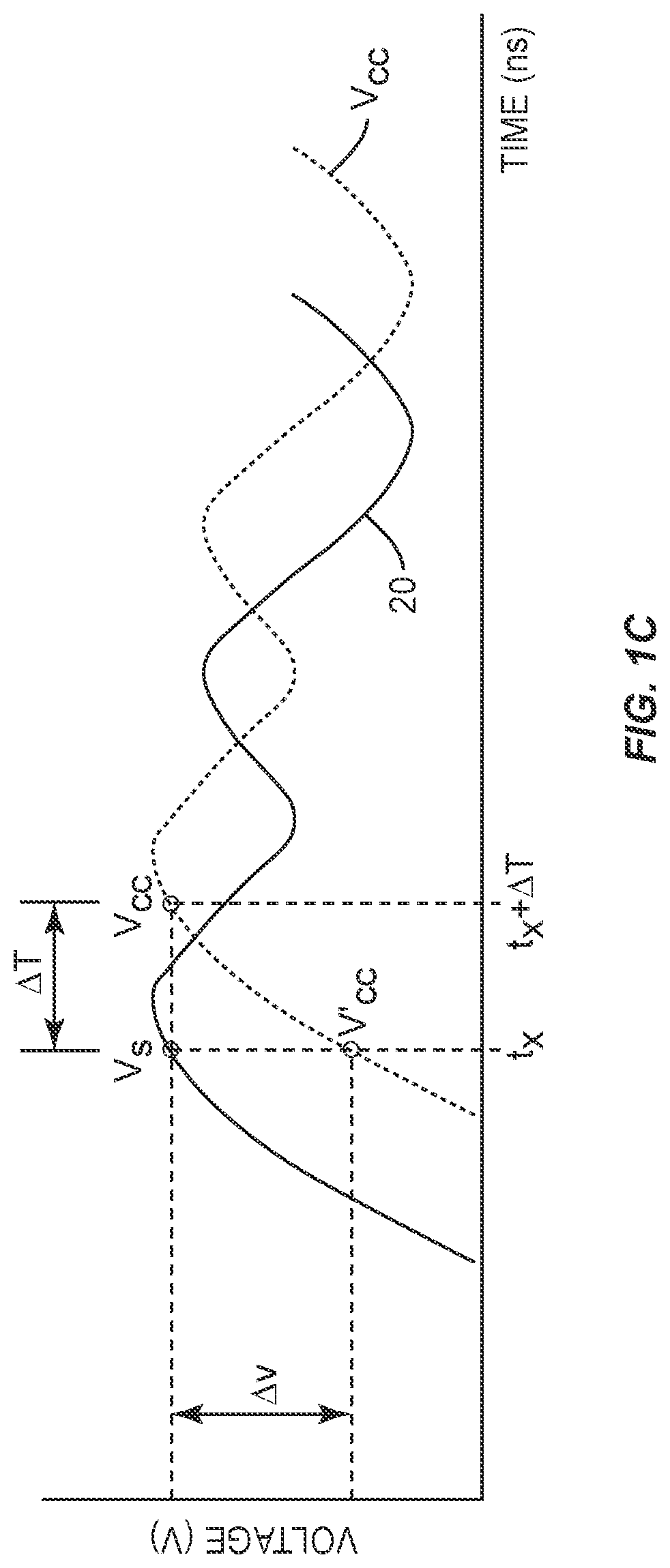
[0013] FIG. 1C is a graphic diagram providing an exemplary illustration as to how the inherent processing delay in the existing PMIC of FIG. 1A can cause the amplitude distortion in the analog signal;
[0014] FIG. 2 is a schematic diagram of an exemplary PMIC configured according to embodiments of the present disclosure to offset various group delays incurred in the PMIC;
[0015] FIG. 3 is a graphic diagram providing an exemplary illustration of an inverted time-variant target voltage that is time-adjusted relative to a time-variant envelope to substantially offset a group delay(s);
[0016] FIG. 4A is a schematic diagram of a conventional inverted amplifier circuit;
[0017] FIG. 4B is a schematic diagram of a conventional non-inverted amplifier circuit;
[0018] FIG. 5 is a schematic diagram of an exemplary inverted group delay circuit configured according to an embodiment of the present disclosure;
[0019] FIG. 6A is a schematic diagram providing an exemplary illustration of the inverted group delay circuit of FIG. 5 operable to offset a negative group delay;
[0020] FIG. 6B is a schematic diagram providing an exemplary illustration of the inverted group delay circuit of FIG. 5 operable to offset a positive group delay; and
[0021] FIG. 7 is a schematic diagram providing an exemplary differential inverted group delay circuit.
DETAILED DESCRIPTION
[0022] The embodiments set forth below represent the necessary information to enable those skilled in the art to practice the embodiments and illustrate the best mode of practicing the embodiments. Upon reading the following description in light of the accompanying drawing figures, those skilled in the art will understand the concepts of the disclosure and will recognize applications of these concepts not particularly addressed herein. It should be understood that these concepts and applications fall within the scope of the disclosure and the accompanying claims.
[0023] It will be understood that, although the terms first, second, etc. may be used herein to describe various elements, these elements should not be limited by these terms. These terms are only used to distinguish one element from another. For example, a first element could be termed a second element, and, similarly, a second element could be termed a first element, without departing from the scope of the present disclosure. As used herein, the term "and/or" includes any and all combinations of one or more of the associated listed items.
[0024] It will be understood that when an element such as a layer, region, or substrate is referred to as being "on" or extending "onto" another element, it can be directly on or extend directly onto the other element or intervening elements may also be present. In contrast, when an element is referred to as being "directly on" or extending "directly onto" another element, there are no intervening elements present. Likewise, it will be understood that when an element such as a layer, region, or substrate is referred to as being "over" or extending "over" another element, it can be directly over or extend directly over the other element or intervening elements may also be present. In contrast, when an element is referred to as being "directly over" or extending "directly over" another element, there are no intervening elements present. It will also be understood that when an element is referred to as being "connected" or "coupled" to another element, it can be directly connected or coupled to the other element or intervening elements may be present. In contrast, when an element is referred to as being "directly connected" or "directly coupled" to another element, there are no intervening elements present.
[0025] Relative terms such as "below" or "above" or "upper" or "lower" or "horizontal" or "vertical" may be used herein to describe a relationship of one element, layer, or region to another element, layer, or region as illustrated in the Figures. It will be understood that these terms and those discussed above are intended to encompass different orientations of the device in addition to the orientation depicted in the Figures.
[0026] The terminology used herein is for the purpose of describing particular embodiments only and is not intended to be limiting of the disclosure. As used herein, the singular forms "a," "an," and "the" are intended to include the plural forms as well, unless the context clearly indicates otherwise. It will be further understood that the terms "comprises," "comprising," "includes," and/or "including" when used herein specify the presence of stated features, integers, steps, operations, elements, and/or components, but do not preclude the presence or addition of one or more other features, integers, steps, operations, elements, components, and/or groups thereof.
[0027] Unless otherwise defined, all terms (including technical and scientific terms) used herein have the same meaning as commonly understood by one of ordinary skill in the art to which this disclosure belongs. It will be further understood that terms used herein should be interpreted as having a meaning that is consistent with their meaning in the context of this specification and the relevant art and will not be interpreted in an idealized or overly formal sense unless expressly so defined herein.
[0028] Aspects disclosed in the detailed description include an inverted group delay circuit. The inverted group delay circuit can offset a group delay between a pair of signals. In a non-limiting example, the inverted group delay circuit can be configured to offset a group delay (e.g., negative group delay) between a time-variant voltage and a time-variant envelope of an analog signal. More specifically, the inverted group delay circuit can output an inverted time-variant voltage having an opposing phase and time-adjusted relative to the time-variant voltage to thereby offset the group delay between the time-variant voltage and the time-variant envelope. As such, the inverted group delay circuit can be provided in a power management integrated circuit (PMIC) to improve timing alignment between a time-variant voltage(s) and a time-variant analog signal(s) at a power amplifier(s), thus helping to reduce potential amplitude distortion when the analog signal(s) is amplified by the power amplifier(s).
[0029] Before discussing a PMIC employing the inverted group circuit of the present disclosure, starting at FIG. 2, a brief overview of an existing PMIC that may cause amplitude distortion in an analog signal as a result of an inherent processing delay associated with the existing PMIC is first provided with reference to FIGS. 1A-1C.
[0030] FIG. 1A is a schematic diagram of an exemplary existing PMIC 10 that that may cause amplitude distortion in an analog signal 12 as a result of an inherent processing delay in the existing PMIC 10. The existing PMIC 10 is configured to provide a time-variant voltage V.sub.CC to a power amplifier 14 for amplifying the analog signal 12. The analog signal 12 may be generated by a transceiver circuit 16 and provided to a signal processing circuit 18 in an intermediate frequency (IF). The signal processing circuit 18 may upconvert the analog signal 12 from the IF to a carrier frequency and provide the analog signal 12 to the power amplifier 14 for amplification.
[0031] The analog signal 12 is associated with a time-variant envelope 20 that rises and falls over time. Thus, to prevent potential amplitude distortion in the analog signal 12 and ensure higher operating efficiency of the power amplifier 14, it is necessary for the existing PMIC 10 to generate the time-variant voltage V.sub.CC to closely track the time-variant envelope 20.
[0032] In other words, the time-variant voltage V.sub.CC needs to be aligned with the time-variant envelope 20 as closely as possible. As such, the existing PMIC 10 is configured to include a target voltage circuit 22 and an envelope tracking (ET) integrated circuit (ETIC) 24. The target voltage circuit 22 includes an envelope detector circuit 26 and an analog lookup table (LUT) circuit 28. The envelope detector circuit 26 is configured to detect the time-variant envelope 20 of the analog signal 12 and provide a detected time-variant envelope 20' to the analog LUT circuit 28. The analog LUT circuit 28 is configured to generate a target voltage V.sub.TGT from the detected time-variant envelope 20' and provide the target voltage V.sub.TGT to the ETIC 24. The ETIC 24, in turn, generates the time-variant voltage V.sub.CC based on the target voltage V.sub.TGT.
[0033] In this regard, since the target voltage V.sub.TGT tracks the detected time-variant envelope 20' and the time-variant voltage V.sub.CC tracks the target voltage V.sub.TGT, the time-variant voltage V.sub.CC will end up rising and falling along with the time-variant envelope 20. Notably, the envelope detector circuit 26 and the analog LUT circuit 28 can cause an inherent processing delay. As a result, as shown in FIG. 1B, the detected time-variant envelope 20' will lag behind the time-variant envelope 20 associated with the analog signal 12 and the target voltage V.sub.TGT will lag behind the detected time-variant envelope 20'.
[0034] FIG. 1B is a graphic diagram providing an exemplary illustration of a group delay .DELTA.T between the time-variant envelope 20 of the analog signal 12 and the target voltage V.sub.TGT caused by the inherent processing delay in the existing PMIC 10 of FIG. 1A. Common elements between FIGS. 1A and 1B are shown therein with common element numbers and will not be re-described herein.
[0035] As shown in FIG. 1B, the detected time-variant envelope 20' is delayed from the time-variant envelope 20 of the analog signal 12 by a first temporal delay .DELTA.T.sub.1, and the target voltage V.sub.TGT is delayed from the detected time-variant envelope 20' by a second temporal delay .DELTA.T.sub.2. The group delay .DELTA.T, which refers generally to an actual transit time of a signal (e.g., the target voltage V.sub.TGT or the time-variant voltage V.sub.CC) through a device (e.g., the conventional PMIC 10) under test as a function of frequency, can thus include the first temporal delay .DELTA.T.sub.1, the second temporal delay .DELTA.T.sub.2, and/or the inherent processing delay of the ETIC 24. Understandably, the group delay .DELTA.T can cause timing misalignment between the time-variant voltage V.sub.CC and the time-variant envelope 20 at the power amplifier 14.
[0036] As illustrated in FIG. 1C, the misalignment between the time-variant voltage V.sub.CC and the time-variant envelope 20 of the analog signal 12 can cause amplitude distortion in the analog signal 12. FIG. 1C is a graphic diagram providing an exemplary illustration as to how the inherent processing delay in the existing PMIC 10 of FIG. 1A can cause amplitude distortion in the analog signal 12.
[0037] If the time-variant envelope 20 and the time-variant voltage V.sub.CC are perfectly aligned, an instantaneous amplitude of the analog signal 12 (not shown), which is represented by a voltage Vs, would substantially equal the time-variant voltage V.sub.CC at time t.sub.x. However, as shown in FIG. 1C, the time-variant voltage V.sub.CC lags behind the time-variant envelope 20 by the group delay .DELTA.T. As such, at time t.sub.x, the power amplifier 14 (not shown) receives a lower voltage V'.sub.CC, instead of the time-variant voltage V.sub.CC. In this regard, the time-variant voltage V.sub.CC deviates from the time-variant envelope 20 by a voltage differential .DELTA.v at time t.sub.x. Consequently, the power amplifier 14 may clip the analog signal 12 to cause an amplitude distortion. As such, it is desirable to reduce the misalignment between the time-variant voltage V.sub.CC and the time-variant envelope 20 of the analog signal 12 as much as possible.
[0038] In this regard, FIG. 2 is a schematic diagram of an exemplary PMIC 30 configured according to embodiments of the present disclosure to offset various group delays incurred in the PMIC 30.
[0039] The PMIC 30 is configured to provide a time-variant voltage V.sub.CC to a power amplifier 32 for amplifying an analog signal 34. The analog signal 34 may be generated by a transceiver circuit 36 and provided to a signal processing circuit 38 in the IF. The signal processing circuit 38 may upconvert the analog signal 34 from the IF to a carrier frequency and provide the analog signal 34 to the power amplifier 32 for amplification.
[0040] The analog signal 34 is associated with a time-variant envelope 40 that rises and falls over time. Thus, to prevent potential amplitude distortion in the analog signal 34 and ensure higher operating efficiency of the power amplifier 32, it is necessary to generate the time-variant voltage V.sub.CC to closely track the time-variant envelope 40.
[0041] In this regard, the PMIC 30 is configured to include a target voltage circuit 42. As discussed below, the target voltage circuit 42 is configured to generate an inverted time-variant target voltage V.sub.TGT-R(t) that is time-adjusted relative to the time-variant envelope 40 of the analog signal 34 to offset a group delay(s) incurred in the PMIC 30. Herein, a first signal is said to be time-adjusted relative to a second signal when the first signal is advanced in time to eliminate a negative group delay from the second signal or delayed in time to eliminate a positive group delay from the second signal.
[0042] Accordingly, an ETIC 44 in the PMIC 30 can generate a time-variant voltage V.sub.CC based on the inverted time-variant target voltage V.sub.TGT-R(t) and provide the time-variant voltage V.sub.CC to the power amplifier 32 for amplifying the analog signal 34. Since the inverted time-variant target voltage V.sub.TGT-R(t) is better aligned with the time-variant envelope 40, the time-variant voltage V.sub.CC will be better aligned with the time-variant envelope 40 as a result. Therefore, it is possible to reduce or even avoid potential amplitude distortion to the analog signal 34 during amplification.
[0043] In a non-limiting example, the target voltage circuit 42 includes an envelope detector circuit 46 and an analog LUT circuit 48. The envelope detector circuit 46 is configured to detect the time-variant envelope 40 of the analog signal 34 and provide a detected time-variant envelope 40' to the analog LUT circuit 48. The analog LUT circuit 48 is configured to generate a target voltage V.sub.TGT(t) based on the detected time-variant envelope 40' of the analog signal 34. Like the envelope detector circuit 26 and the analog LUT circuit 28 in the existing PMIC 10 of FIG. 1A, the envelope detector circuit 46 and the analog LUT circuit 48 can each cause certain processing delays. As a result, the detected time-variant envelope 40' may be delayed from the time-variant envelope 40 of the analog signal 34 by a first temporal delay .DELTA.T.sub.1 and the target voltage V.sub.TGT(t) may be delayed from the detected time-variant envelope 40' by a second temporal delay .DELTA.T.sub.2. In addition, the ETIC 44 can also incur a certain processing delay that may further delay the time-variant voltage V.sub.CC from the target voltage V.sub.TGT(t) by a third temporal delay .DELTA.T.sub.3. As a result, the time-variant voltage V.sub.CC may become misaligned from the time-variant envelope 40 by the group delay .DELTA.T that includes the first temporal delay .DELTA.T.sub.1, the second temporal delay .DELTA.T.sub.2, and the third temporal delay .DELTA.T.sub.3.
[0044] In an embodiment, the target voltage circuit 42 is configured to include an inverted group delay circuit 50. As shown in FIG. 3, the inverted group delay circuit 50 is configured to generate the inverted time-variant target voltage V.sub.TGT(t).sub.-R(t), which is time-adjusted relative to the time-variant envelope 40 of the analog signal to offset the group delay .DELTA.T that includes at least the first temporal delay .DELTA.T.sub.1 and the second temporal delay .DELTA.T.sub.2.
[0045] FIG. 3 is a graphic diagram providing an exemplary illustration of the inverted time-variant target voltage V.sub.TGT-R(t) that is time-adjusted relative to the time-variant envelope 40 to substantially offset the first temporal delay .DELTA.T.sub.1 and the second temporal delay .DELTA.T.sub.2. Common elements between FIGS. 2 and 3 are shown therein with common element numbers and will not be re-described herein.
[0046] As shown in FIG. 3, the target voltage V.sub.TGT(t) as originally generated by the analog LUT circuit 48 lags behind the time-variant envelope 40 by the group delay .DELTA.T that includes a sum of the first temporal delay .DELTA.T.sub.1 and the second temporal delay .DELTA.T.sub.2. In contrast, the inverted time-variant target voltage V.sub.TGT-R(t) is time-adjusted to substantially offset the first temporal delay .DELTA.T.sub.1 and the second temporal delay .DELTA.T.sub.2 to thereby be better aligned with the time-variant envelope 40. Herein, the inverted time-variant target voltage V.sub.TGT-R(t) is said to substantially offset the first temporal delay .DELTA.T.sub.1 and the second temporal delay .DELTA.T.sub.2 when a temporal gap .DELTA.T between the inverted time-variant target voltage V.sub.TGT-R(t) and the time-variant envelope 40 is less than 10% of the group delay .DELTA.T. As a result of improved alignment with the time-variant envelope 40, it is possible to reduce or even avoid amplitude distortion at the power amplifier 32.
[0047] Before discussing the inverted group delay circuit 50 of the present disclosure, starting at FIG. 5, a brief overview of inverted and non-inverted amplifiers is first provided with reference to FIGS. 4A and 4B, respectively.
[0048] FIG. 4A is a schematic diagram of a conventional inverted amplifier circuit 52. The conventional inverted amplifier circuit 52 receives an input voltage V.sub.IN via a voltage input 54 and outputs an inverted output voltage V.sub.OUT via a voltage output 56. The conventional inverted amplifier circuit 52 also includes an operational amplifier 58, which includes an inverting terminal 60, a non-inverting terminal 62, and an output terminal 64. The inverting terminal 60 is coupled to the voltage input 54 via an input resistor R.sub.IN to receive the input voltage V.sub.IN. The non-inverting terminal 62 is coupled to a ground (GND). The output terminal 64 is coupled to the voltage output 56. The conventional inverted amplifier circuit 52 also includes a feedback resistor RF that is coupled between the inverting terminal 60 and the output terminal 64.
[0049] The conventional inverted amplifier circuit 52 is configured to output the inverted output voltage V.sub.OUT that is 180.degree. out of phase from the input voltage V.sub.IN. The conventional inverted amplifier circuit 52 generates a voltage gain A.sub.V as shown in equation (Eq. 1) below.
A.sub.V=V.sub.OUT/V.sub.IN=-R.sub.F/R.sub.IN (Eq. 1)
[0050] FIG. 4B is a schematic diagram of a conventional non-inverted amplifier circuit 66. The conventional non-inverted amplifier circuit 66 receives an input voltage V.sub.IN via a voltage input 68 and outputs a non-inverted output voltage V.sub.OUT via a voltage output 70. The conventional non-inverted amplifier circuit 66 also includes an operational amplifier 72, which includes an inverting terminal 74, a non-inverting terminal 76, and an output terminal 78. The non-inverting terminal 76 is coupled to the voltage input 68 to receive the input voltage V.sub.IN. The inverting terminal 74 is coupled to the GND via an input resistor R.sub.IN. The output terminal 78 is coupled to the voltage output 56. The conventional non-inverted amplifier circuit 66 also includes a feedback resistor R.sub.F that is coupled between the inverting terminal 74 and the output terminal 78.
[0051] The conventional non-inverted amplifier circuit 66 is configured to output the inverted output voltage V.sub.OUT that is in phase with the input voltage V.sub.IN. The conventional non-inverted amplifier circuit 66 generates a voltage gain A.sub.V as shown in equation (Eq. 2) below.
A.sub.V=V.sub.OUT/V.sub.IN=(1+R.sub.F/R.sub.IN) (Eq. 2)
[0052] FIG. 5 is a schematic diagram of an exemplary inverted group delay circuit 80 configured according to an embodiment of the present disclosure and can be provided in the PMIC 30 of FIG. 2 as the inverted group delay circuit 50. Common elements between FIGS. 2 and 5 are shown therein with common element numbers and will not be re-described herein.
[0053] In a specific embodiment disclosed herein, the inverted group delay circuit 80 is configured to offset the group delay .DELTA.T between the time-variant target voltage V.sub.TGT(t) or the time-variant voltage V.sub.CC(t) and the time-variant envelope 40 of the analog signal 34. However, it should be appreciated that the inverted group delay circuit 80 can be configured flexibly and utilized broadly to correct a positive group delay .DELTA.T and/or a negative group delay -.DELTA.T between any pair of signals.
[0054] In a non-limiting example, the inverted group delay circuit 80 includes a tunable resistor-capacitor (RC) circuit 82 and an operational amplifier 84. The tunable RC circuit 82 includes a first voltage input 86 and a second voltage input 88 each coupled to a switch circuit 90. The tunable RC circuit 82 also includes a resistor R.sub.1 and a tunable capacitor C.sub.1 that are coupled in parallel between a common node 92 and the switch circuit 90. For example, the switch circuit 90 includes a first switch S.sub.1 and a second switch S.sub.2. The first switch S.sub.1 is coupled between the first voltage input 86 and the second voltage input 88. The second switch S.sub.2 is coupled between the second voltage input 88 and the tunable capacitor C.sub.1. Although the inverted group delay circuit 80 is shown to include the tunable capacitor C.sub.1, it should be appreciated that the tunable capacitor C.sub.1 can be replaced by a tunable resistor.
[0055] In examples discussed herein, the tunable RC circuit 82 is configured to output a time-variant voltage V.sub.TGT(t), which is equivalent to and referred interchangeably as the time-variant target voltage V.sub.TGT(t) in FIG. 2. In this regard, according to the previous discussion in FIG. 2, the time-variant target voltage V.sub.TGT(t) is delayed from the time-variant envelope 40 of the analog signal 34 by the group delay .DELTA.T.
[0056] The operational amplifier 84 includes an inverting terminal 94, a non-inverting terminal 96, and an output terminal 98. The output terminal 98 is coupled to the inverting terminal 94 via a feedback resistor R.sub.2.
[0057] The inverting terminal 94 is coupled to the common node 92 to receive the time-variant target voltage V.sub.TGT(t). The non-inverting terminal 96 is configured to receive a reference voltage V.sub.REF so determined to keep the operational amplifier 84 operating in a respective linear region. In a non-limiting example, the reference voltage V.sub.REF can be set to 0 V. The output terminal 98 is coupled to a voltage output 100 and configured to output an inverted time-variant voltage -V.sub.TGT-R(t), which is equivalent to and referred interchangeably as the inverted time-variant target voltage V.sub.TGT-R(t) in FIG. 2. The inverted time-variant target voltage -V.sub.TGT-R(t) is so generated to have an opposing phase (180.degree. phase offset) and be time-adjusted relative to the time-variant target voltage V.sub.TGT(t) to thereby offset the group delay .DELTA.T, which can be a positive group delay .DELTA.T or a negative group delay -.DELTA.T.
[0058] In a non-limiting example, the inverted group delay circuit 80 further includes a control circuit 102, which can be a field-programmable gate array (FPGA), as an example. The control circuit 102 can be configured to determine the group delay .DELTA.T between the time-variant target voltage V.sub.TGT(t) and the time-variant envelope 40 of the analog signal 34. In a non-limiting example, the group delay .DELTA.T can be predetermined (e.g., during fabrication and/or calibration) and stored in the control circuit 102. Accordingly, the control circuit 102 can control the tunable RC circuit 82 to output the time-variant target voltage V.sub.TGT(t) with the group delay .DELTA.T.
[0059] In one embodiment, the inverted group delay circuit 80 can be configured to output the inverted time-variant target voltage V.sub.TGT-R(t) that is time-adjusted to offset a negative group delay -.DELTA.T. In this regard, the tunable RC circuit 82 can be configured to receive a positive time-variant target voltage V.sub.TGT(t) via the first voltage input 86. The control circuit 102 may close the first switch S.sub.1 to couple the first voltage input 86 to the resistor R.sub.1 and the tunable capacitor C.sub.1, while concurrently opening the second switch S.sub.2 to decouple the second voltage input 88 from the resistor R.sub.1 and the tunable capacitor C.sub.1.
[0060] FIG. 6A is a schematic diagram providing an exemplary illustration of the inverted group delay circuit 80 of FIG. 5 operable to offset the negative group delay -.DELTA.T. Common elements between FIGS. 5 and 6A are shown therein with common element numbers and will not be re-described herein.
[0061] In a non-limiting example, the inverted group delay circuit 80 operable according to FIG. 6A can implement a transfer function H(s) as expressed in equation (Eq. 3) below.
H(s)=-(R.sub.2/R.sub.1)*(1+R.sub.1*C.sub.1*s) (Eq. 3)
[0062] In the equation (Eq. 3) above, s represents a Laplace notation that defines a frequency characteristic of a filter or a network. Notably, the negative group delay -.DELTA.T is a function of the RC constant .tau. (.tau.=R.sub.1C.sub.1) of the tunable RC circuit 82. In this regard, the control circuit 102 may control the tunable capacitor C.sub.1 to flexibly adjust the negative group delay -.DELTA.T. Thus, in accordance with the transfer function H(s) above, the inverted group delay circuit 80 can generate the inverted time-variant target voltage -V.sub.TGT-R(.tau.-.DELTA.T) that is time-advanced to offset the negative group delay -.DELTA.T.
[0063] In another embodiment, the inverted group delay circuit 80 can be configured to output the inverted time-variant target voltage V.sub.TGT-R(t) that is time-adjusted to offset a positive group delay .DELTA.T. In this regard, the tunable RC circuit 82 can be configured to receive a positive time-variant target voltage V.sub.TGT(t) via the first voltage input 86 and a negative time-variant target voltage -V.sub.TGT(t) via the second voltage input 88. The control circuit 102 may open the first switch S.sub.1 to decouple the first voltage input 86 from the tunable capacitor C.sub.1, while concurrently closing the second switch S.sub.2 to couple the second voltage input 88 to the tunable capacitor C.sub.1.
[0064] FIG. 6B is a schematic diagram providing an exemplary illustration of the inverted group delay circuit 80 of FIG. 5 operable to offset the positive group delay .DELTA.T. Common elements between FIGS. 5 and 6B are shown therein with common element numbers and will not be re-described herein.
[0065] In a non-limiting example, the inverted group delay circuit 80 operable according to FIG. 6B can implement a transfer function H(s) as expressed in equation (Eq. 4) below.
H(s)=-(R.sub.2/R.sub.1)*(1-R.sub.1*C.sub.1*s) (Eq. 4)
[0066] Notably, the positive group delay .DELTA.T is a function of the RC constant .tau. (.tau.=R.sub.1C.sub.1) of the tunable RC circuit 82. In this regard, the control circuit 102 may control the tunable capacitor C.sub.1 to flexibly adjust the positive group delay .DELTA.T. Thus, in accordance with the transfer function H(s) above, the inverted group delay circuit 80 can generate the inverted time-variant target voltage -V.sub.TGT-R(.tau.+.DELTA.T) that is time-delayed to offset the positive group delay .DELTA.T.
[0067] With reference back to FIG. 2, alternative to predetermining and storing the group delay d .DELTA.T in the control circuit 102, the target voltage circuit 42 may be configured to include a delay detector circuit 104 to dynamically determine the group delay .DELTA.T. In one non-limiting example, the delay detector circuit 104 can detect the group delay .DELTA.T that includes the first temporal delay .DELTA.T.sub.1 and the second temporal delay .DELTA.T.sub.2. In another non-limiting example, the delay detector circuit 104 can detect the group delay .DELTA.T that includes the first temporal delay .DELTA.T.sub.1, the second temporal delay .DELTA.T.sub.2, and the third temporal delay .DELTA.T.sub.3. Accordingly, the delay detector circuit 104 provides the determined group delay .DELTA.T to the inverted group delay circuit 50.
[0068] In a non-limiting example, it is possible to employ a pair of the inverted group delay circuit 80 in FIG. 5 to form a differential inverted group delay circuit. In this regard, FIG. 7 is a schematic diagram of an exemplary differential inverted group delay circuit 106 that includes a pair of the inverted group delay circuit 80 of FIG. 5. Common elements between FIGS. 5 and 7 are shown therein with common element numbers and will not be re-described herein.
[0069] The differential inverted grope delay circuit 106 includes a positive inverted group delay circuit 80P and a negative inverted group delay circuit 80N. In this regard, the differential inverted group delay circuit 106 can be employed to offset the group delay .DELTA.T when the power amplifier 32 is a differential power amplifier.
[0070] Each of the positive inverted group delay circuit 80P and the negative inverted group delay circuit 80N is the same as the inverted group delay circuit 80 of FIG. 5, which includes the tunable RC circuit 82 and the operational amplifier 84. The positive inverted group delay circuit 80P is configured to output a positive inverted time-variant voltage V.sub.TGT-R(.tau.) at a positive voltage output 108P. The negative inverted group delay circuit 80N is configured to output a negative inverted time-variant voltage -V.sub.TGT-R(.tau.) at a negative voltage output 108N. In a non-limiting example, the tunable RC circuit 82 in each of the positive inverted group delay circuit 80P and the negative inverted group delay circuit 80N is coupled to the first voltage input 86 and the second voltage input 88 via a switch circuit 110.
[0071] Those skilled in the art will recognize improvements and modifications to the embodiments of the present disclosure. All such improvements and modifications are considered within the scope of the concepts disclosed herein and the claims that follow.
* * * * *
D00000
D00001
D00002
D00003
D00004
D00005
D00006
D00007
D00008
D00009
XML
uspto.report is an independent third-party trademark research tool that is not affiliated, endorsed, or sponsored by the United States Patent and Trademark Office (USPTO) or any other governmental organization. The information provided by uspto.report is based on publicly available data at the time of writing and is intended for informational purposes only.
While we strive to provide accurate and up-to-date information, we do not guarantee the accuracy, completeness, reliability, or suitability of the information displayed on this site. The use of this site is at your own risk. Any reliance you place on such information is therefore strictly at your own risk.
All official trademark data, including owner information, should be verified by visiting the official USPTO website at www.uspto.gov. This site is not intended to replace professional legal advice and should not be used as a substitute for consulting with a legal professional who is knowledgeable about trademark law.