Display Device And Image Sensing Method Thereof
CHUNG; Jun-Wen ; et al.
U.S. patent application number 17/464742 was filed with the patent office on 2022-04-14 for display device and image sensing method thereof. The applicant listed for this patent is Guangzhou Tyrafos Semiconductor Technologies Co., Ltd.. Invention is credited to Jun-Wen CHUNG, Hsu-Wen Fu.
| Application Number | 20220115443 17/464742 |
| Document ID | / |
| Family ID | |
| Filed Date | 2022-04-14 |


| United States Patent Application | 20220115443 |
| Kind Code | A1 |
| CHUNG; Jun-Wen ; et al. | April 14, 2022 |
DISPLAY DEVICE AND IMAGE SENSING METHOD THEREOF
Abstract
The invention relates to a display device, applicable to fingerprint image recognition. The display device includes: a substrate, a cover panel, and unit pixels. First, the unit pixels on the display device emit light alternately. When a part of the unit pixels emit light, defined as in a light-emitting state, and when another part of the unit pixels do not emit light, defined as in a sensing state; then, the unit pixels in the light-emitting state are used as the light-emitting area; the unit pixels in the sensing state are used as the sensing area; the unit pixels in the light-emitting area emit incident light to and reflected by a test object; the unit pixels in the sensing area sense the reflected light, and generates an image electrical signal. Therefore, the display device can be used as both a light-emitting element and a sensing element for fingerprint image recognition.
| Inventors: | CHUNG; Jun-Wen; (Tainan City, TW) ; Fu; Hsu-Wen; (Kaohsiung City, TW) | ||||||||||
| Applicant: |
|
||||||||||
|---|---|---|---|---|---|---|---|---|---|---|---|
| Appl. No.: | 17/464742 | ||||||||||
| Filed: | September 2, 2021 |
Related U.S. Patent Documents
| Application Number | Filing Date | Patent Number | ||
|---|---|---|---|---|
| 63089055 | Oct 8, 2020 | |||
| International Class: | H01L 27/28 20060101 H01L027/28; H04N 5/378 20060101 H04N005/378; G06K 9/00 20060101 G06K009/00; G06K 9/20 20060101 G06K009/20 |
Claims
1. A display device, applicable to an environment for sensing fingerprint images, comprising: a substrate, having an upper surface and a lower surface; a cover panel, disposed on the upper surface of the substrate; and a plurality of unit pixels, disposed on the substrate, the unit pixels comprising a plurality of red unit pixels, a plurality of green unit pixels, and a plurality of blue unit pixels, wherein the red unit pixels emitting a red incident light, the green unit pixels emitting a green incident light, and the blue unit pixels emitting a blue incident light; wherein, the unit pixels on the display device emitting light alternately; and when a part of the unit pixels emitting light, defined as in a light-emitting state, when the other part of the unit pixels not emitting light, defined as in a sensing state, the unit pixels in the light-emitting state being regarded as a light-emitting area, and the unit pixels in the sensing state being regarded as a sensing area, a part of the unit pixels in the light-emitting area emitting an incident light to a test object, the test object reflecting the incident light to generate a reflected light, and a part of the unit pixels in the sensing area receiving the reflected light to generate an image electrical signal.
2. The display device according to claim 1, wherein the display device is an organic light-emitting diode display device.
3. The display device according to claim 1, wherein the light-emitting area comprises only the blue unit pixels of the plurality of unit pixels.
4. The display device according to claim 1, wherein the sensing area comprises one or a combination of the red unit pixels and the green unit pixels of the plurality of unit pixels.
5. The display device according to claim 1, wherein the plurality of unit pixels are disposed between the upper surface of the substrate and the cover panel.
6. The display device according to claim 1, wherein the plurality of unit pixels are disposed on the lower surface of the substrate.
7. The display device according to claim 1, wherein the display device further comprises a readout circuit coupled to each of the unit pixels, and the readout circuit receives the image electrical signal to generate a corresponding image information.
8. An image sensing method, comprising the following steps of: a definition step: a plurality of unit pixels on a display device emitting light alternately; when a part of the unit pixels emitting light, these unit pixels being defined as in a light-emitting state, and when another part of the unit pixels not emitting light, these unit pixels being defined as in a sensing state; a light-emitting area step: the unit pixels in the light-emitting state being used as a light-emitting area; a sensing area step: the unit pixels in the sensing state being used as a sensing area; an emission step: a part of the unit pixels in the light-emitting area emitting an incident light to a test object, and the incident light emitted to the test object being reflected to generate a reflected light; a sensing step: a part of the unit pixels in the sensing area sensing the reflected light, and the sensing area generating a corresponding image electrical signal.
9. The image sensing method according to claim 8, wherein the display device is one of an organic light-emitting diode display device and a micro light-emitting diode display device.
10. The image sensing method according to claim 8, wherein the light-emitting area comprises only a plurality of blue unit pixels of the plurality of unit pixels.
11. The image sensing method according to claim 8, wherein the sensing area comprises one or a combination of a plurality of red unit pixels and a plurality of green unit pixels of the plurality of unit pixels.
Description
CROSS-REFERENCE TO RELATED APPLICATION
[0001] This application claims the priority of U.S. provisional patent application No. 63/089,055, filed on Oct. 8, 2020, which is incorporated herewith by reference.
BACKGROUND OF THE INVENTION
1. Field of the Invention
[0002] The present invention relates generally to a display device, and more particularly to a display device and an image sensing method applicable to fingerprint image recognition.
2. The Prior Arts
[0003] With the development of mobile phone technology and the continuous growing demands from mobile phone users, the display screen of the smart phone has been developed towards a full-screen design for a better user experience, wherein, to provide unlock recognition, under-screen optical fingerprint recognition is currently a common solution on the market, which is not only used in smart phones, but also building fingerprint recognition systems, corporate attendance fingerprint recognition systems, and so on.
[0004] There are currently three development directions for under-screen fingerprint recognition using Organic Light-Emitting Diode (OLED) screens: (1) arranging at least one thin complementary metal oxide semiconductor (CMOS) sensor directly below the screen to be flatly attached to the bottom of the screen, and the gap between the sub-pixels of the OLED allowing light to pass through, thereby identifying fingerprints. The above technical features are similar to one-piece on glass solution (OGS) or one-piece touch on lens (TOL) of a capacitive touch panel, which can also become a miniature sensor chip and used an imaging lens set to make a lens-based sensor module to be assembled under the display screen; (2) using a thin film transistor process, and using the sensitivity to visible light of amorphous silicon (a-Si:H) and polysilicon (poly-Si) to produce light sensitive elements on a glass substrate or a flexible substrate (such as polyimide film), and mounted under the OLED screen, which can also be used as a sealing glass to seal with the OLED panel to sense fingerprint information. The above technical features are similar to capacitive touch panels, also known as on-cells by those with ordinary knowledge in the art; (3) inserting image sensors between the pixels of OLEDs, an organic photodiode (OPD) being disposed on the thin-film transistor (TFT) substrate, in addition to each set of pixels (R/GB), as a sensing element. The above technical features are similar to capacitive touch panels, also known as in-cell by those with ordinary knowledge in the art.
[0005] However, the problem of using the aforementioned solution (1) is that as users pursue the image quality of display devices, and the design and process technology of OLED display devices mature, the unit pixels on OLED panels are increasing, making the gap between the sub-pixels of the OLED gradually decreasing, and more difficult for the under-screen fingerprint recognition technology to allow the light penetrate through the gaps between the sub-pixels of the OLED, which makes the implementation of the aforementioned solution (1) less feasible. In addition, the problem of using the aforementioned solution (2) is the same as those of the aforementioned solution (1), which makes the implementation of the aforementioned solution (2) more difficult. The problem of using the aforementioned solution (3) is that the technical solution of shrinking the image sensor and inserting it between the pixels of the OLED causes the number of the unit pixels on the OLED panel to decrease, thereby reducing the resolution of the OLED panel.
[0006] Therefore, to address the above-mentioned deficiencies, the inventors disclosed the present invention.
SUMMARY OF THE INVENTION
[0007] A primary objective of the present invention is to provide a display device having a plurality of unit pixels, the unit pixels emit light alternately, and when a part of the unit pixels emit light, the unit pixels are defined as in a light-emitting state, and the other part of the unit pixels not emitting light are defined as in a sensing state. By using the unit pixels in the light-emitting state as the light-emitter for under-screen fingerprint recognition, and the unit pixels in the sensing state as the sensor for under-screen fingerprint recognition, the present invention provides a high-performance image recognition without affecting the panel pixels.
[0008] To achieve the foregoing objective, the present invention provides a display device, applicable to an environment for sensing fingerprint images. The display device comprises: a substrate, having an upper surface and a lower surface; a plurality of unit pixels, arranged on the substrate, the unit pixels comprising a plurality of red unit pixels, a plurality of green unit pixels, and a plurality of blue unit pixels, wherein the red unit pixels emitting a red incident light, the green unit pixels emitting a green incident light, and the blue unit pixels emitting a blue incident light; wherein, the unit pixels on the display device emitting light alternately; and when a part of the unit pixels emitting light, defined as in a light-emitting state, when the other part of the unit pixels not emitting light, defined as in a sensing state, the unit pixels in the light-emitting state being regarded as a light-emitting area, and the unit pixels in the sensing state being regarded as a sensing area, a part of the unit pixels in the light-emitting area emitting an incident light to a test object, the test object reflecting the incident light to generate a reflected light, and a part of the unit pixels in the sensing area receiving the reflected light to generate an image electrical signal.
[0009] Preferably, according to the display device of the present invention, the display device is one of an organic light-emitting diode display device and a micro light-emitting diode display device, but the present invention is not limited hereto.
[0010] Preferably, according to the display device of the present invention, the light-emitting area only includes the blue unit pixels among the unit pixels, but the present invention is not limited hereto.
[0011] Preferably, according to the display device of the present invention, the sensing area only includes the red unit pixels among the unit pixels, but the present invention is not limited hereto.
[0012] Preferably, according to the display device of the present invention, the sensing area includes one or a combination of the red unit pixels and the green unit pixels among the unit pixels, but the present invention is not limited hereto.
[0013] Preferably, according to the display device of the present invention, the unit pixels are disposed between the upper surface of the substrate and the cover panel, but the present invention is not limited hereto.
[0014] Preferably, according to the display device of the present invention, the unit pixels are disposed on the lower surface of the substrate, but the present invention is not limited hereto.
[0015] Preferably, according to the display device of the present invention, the thickness of the cover panel is 700 microns, but the present invention is not limited hereto.
[0016] Preferably, according to the display device of the present invention, the display device further comprises a readout circuit coupled to each of the unit pixels, and the readout circuit receives the image electrical signal and generates a corresponding image information.
[0017] In addition, to achieve the foregoing objective, the present invention, based on the aforementioned display device, further provides an image sensing method, comprising: alternately illuminating a plurality of unit pixels on a display device, wherein, when a part of the unit pixels emitting light, defined as in a light-emitting state, when the other part of the unit pixels not emitting light, defined as in a sensing state, the unit pixels in the light-emitting state being regarded as a light-emitting area, and the unit pixels in the sensing state being regarded as a sensing area, a part of the unit pixels in the light-emitting area emitting an incident light to a test object, the test object reflecting the incident light to generate a reflected light, and a part of the unit pixels in the sensing area receiving the reflected light to generate an image electrical signal.
[0018] Preferably, according to the image sensing method of the present invention, the display device is one of an organic light-emitting diode display device and a micro light-emitting diode display device, but the present invention is not limited hereto.
[0019] In summary, the display device and the image sensing method provided by the present invention mainly rely on the unit pixels to emit light alternately, wherein when a part of the unit pixels emit light, defined as in a light-emitting state; when the other part is not emitting light, defined as in a sensing state; by using the unit pixels in the light-emitting state as the light-emitter for under-screen fingerprint recognition, and the unit pixels in the sensing state as the sensor for under-screen fingerprint recognition, the present invention provides a high-performance image recognition solution without affecting the panel pixels.
[0020] To enable those skilled in the art to understand the purpose, features, and effects of the present invention, the following specific embodiments and accompanying drawings are used to explain the present invention in detail as follows.
BRIEF DESCRIPTION OF THE DRAWINGS
[0021] The present invention will be apparent to those skilled in the art by reading the following detailed description of a preferred embodiment thereto, with reference to the attached drawings, in which:
[0022] FIG. 1 is a schematic view of a display device according to the present invention;
[0023] FIG. 2 is a schematic view of exemplary details of a display device according to the present invention;
[0024] FIG. 3 illustrates the absorption spectrum and emission spectrum of an exemplary host material of the display device according to the present invention;
[0025] FIG. 4 is a schematic view illustrating that the light-emitting area according to the present invention is reflected to the sensing area after emitting light to the test object;
[0026] FIG. 5 is a flowchart illustrating the steps of the image sensing method of the present invention;
[0027] FIG. 6A is a timing diagram illustrating the implementation of the image sensing method of the present invention;
[0028] FIG. 6B is another timing diagram illustrating the implementation of the image sensing method of the present invention;
[0029] FIG. 7 is a schematic view of a display device according to the first embodiment of the present invention;
[0030] FIG. 8 is a flowchart illustrating the steps of performing the image sensing method according to the first embodiment of the present invention
[0031] FIG. 9A is a timing diagram illustrating the implementation of the image sensing method of the present invention;
[0032] FIG. 9B is another timing diagram illustrating the implementation of the image sensing method of the present invention; and
[0033] FIG. 10 is a schematic diagram of a display device according to a second embodiment of the invention.
DETAILED DESCRIPTION OF THE PREFERRED EMBODIMENT
[0034] The accompanying drawings are included to provide a further understanding of the invention, and are incorporated in and constitute a part of this specification. The drawings illustrate embodiments of the invention and, together with the description, serve to explain the principles of the invention.
[0035] FIG. 1 is a schematic view of a display device according to the present invention. As shown in FIG. 1, the display device 100 according to the present invention includes: a substrate 11, a plurality of unit pixel 12, and a cover panel 13. The substrate 11 has an upper surface 111 and a lower surface 112. The cover panel 13 is disposed on the upper surface 111 of the substrate 11. The unit pixels 12 are disposed on the substrate 11.
[0036] Refer to FIG. 2, which shows exemplary details of the display device 100. Specifically, the substrate 11 may be, but is not limited to, a glass substrate, a polyethylene terephthalate (PET) substrate, a cycloolefin polymer (COP) substrate, a transparent polyimide (CPI) substrate, a polyethylene naphthalate (PET) substrate, a Diester (PEN) substrate, a polycarbonate (PC) substrate, a polyether sulfide (PES) substrate, or a polarizing film.
[0037] Specifically, the unit pixels 12 are disposed on the substrate 11. The unit pixels 12 include a red unit pixel 121, a green unit pixel 122, and a blue unit pixel 123, wherein the red unit pixel 121 emits a red incident light R, the green unit pixel 122 emits a green incident light G, and the blue unit pixel 123 emits a blue incident light B.
[0038] Specifically, the wavelength of the red incident light R according to the present invention may be between 620 nm and 750 nm, but the present invention is not limited hereto.
[0039] Specifically, the wavelength of the green incident light G according to the present invention may be between 495 nm and 570 nm, but the present invention is not limited hereto.
[0040] Specifically, the wavelength of the blue incident light B according to the present invention may be between 430 nm and 495 nm, but the present invention is not limited hereto.
[0041] Specifically, referring to FIG. 2, the display device 100 may be an organic light emitting diode display (OLED display). In some embodiments, the unit pixel 12 includes an anode 21, a hole transport layer 22, a light-emitting layer 23, an electron transport layer 24, and a cathode 25. A pixel circuit 14 is provided on the substrate 11, and is coupled to each of the unit pixels 12 to control each of the unit pixels 12. A planarization dielectric layer 15 is provided between the unit pixel 12 and the pixel circuit 14. As shown in FIG. 2, the planarization dielectric layer 15 is provided with barrier wells 16 (bank) fabricated in advance by a yellow light etching process, and the anode 21 of the unit pixel 12 is connected to the corresponding pixel circuit 14 by passing through the via holes between the barrier wells 16. According to some embodiments, the display device 100 further includes an encapsulation layer 17 disposed between the unit pixel 12 and the cover panel 13. The encapsulation layer 17 may be a single-layer of inorganic encapsulation materials, a multilayer stack of inorganic encapsulation materials, or a stack of pairs of inorganic packaging materials and organic packaging materials. The inorganic packaging material used can be, for example, but not limited to, silicon nitride (SiNx), silicon oxide (SiOx), silicon oxynitride (SiONx), aluminum oxide (AlOx), or titanium oxide (TiOx).
[0042] It is worth mentioning that, as shown in FIG. 2, a light-shielding layer 14 may be provided on the substrate 11 and the cover panel 13. The light-shielding layer 14 is used to isolate the background light in the environment from sensing images of the display device 100. In the present invention, the term "isolation" covers both electrical isolation and physical isolation.
[0043] Specifically, refer to FIG. 3, which illustrates the absorption spectrum and the emission spectrum of the host material of the display device according to a preferred embodiment of the present invention. In some embodiments, as shown in FIG. 3, the display device 100 according to the present invention is an organic light-emitting diode display device, but currently the conventional organic light-emitting diode display devices generally use fluorescent materials or phosphorescent materials as the host material for light-emitting layer. The main characteristic of the organic material is that when the molecules inside the material absorb radiant energy higher than its own energy, the electrons are excited from the ground state to an excited state with higher energy, and then the electrons in the excited state decays to the ground state to generate light. It can be understood that the display device 100 according to the present invention can also generate a corresponding image electrical signal by absorbing radiant energy higher than its own energy.
[0044] Specifically, the unit pixels 12 are disposed on the substrate 11. In some embodiments, as shown in FIG. 1, the substrate 11 has an upper surface 111 and a lower surface 112, and the unit pixels 12 are disposed between the upper surface 111 of the substrate 11 and the cover panel 13. In other embodiments, the unit pixels 12 may be disposed on the lower surface 112 of the substrate 11.
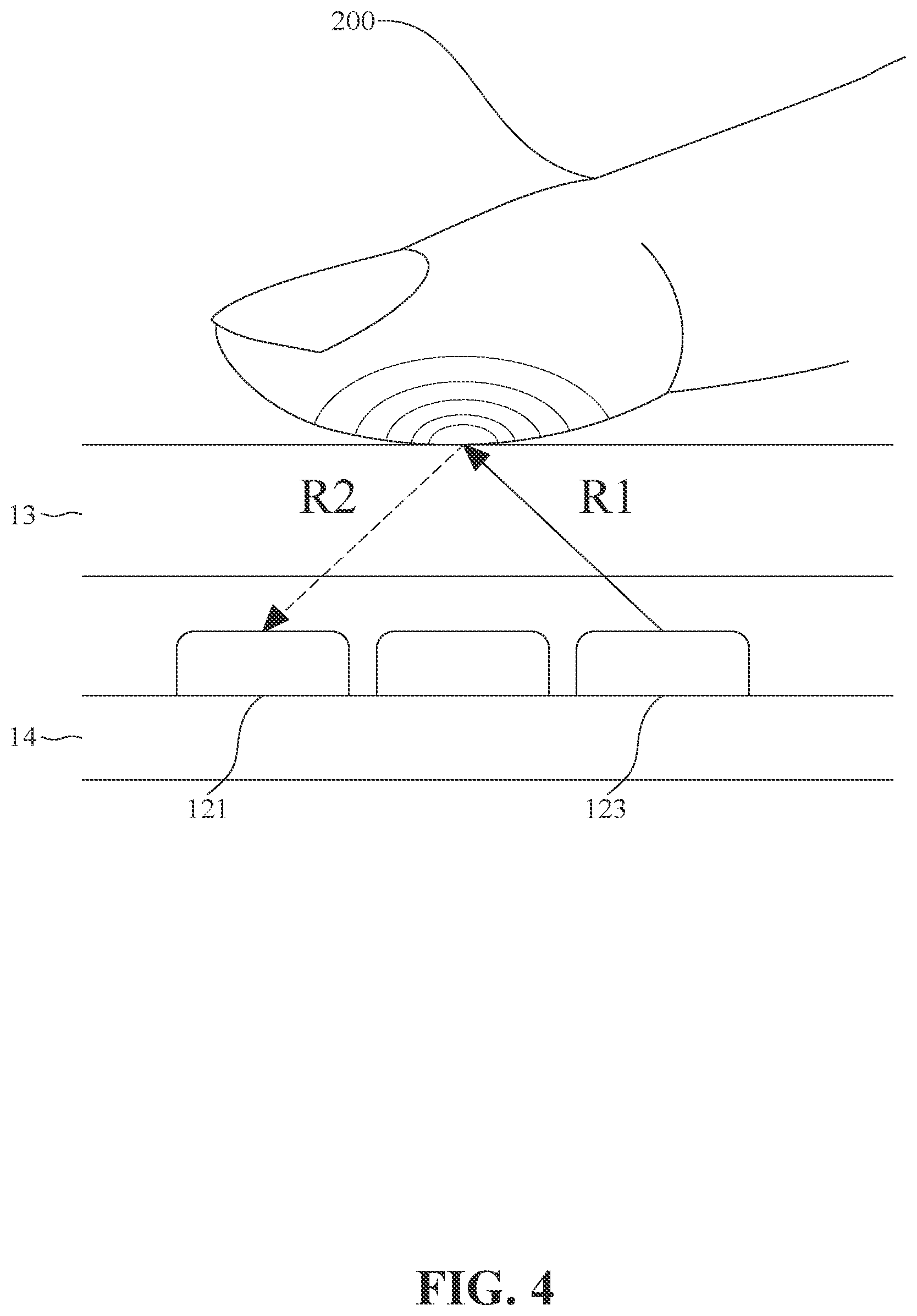
[0045] Specifically, please refer to FIG. 4, which is a schematic view illustrating that light emitted from the light-emitting area is reflected to the sensing area after irradiating onto the test object to be measured. The unit pixels 12 on the display device 100 emit light alternately. When a part of the unit pixels 12 emit light, the unit pixels are said to be in a light-emitting state (not shown). At the same time, when another part of the unit pixels 12 do not emit light, the unit pixels are said to be in a sensing state. As shown in FIG. 4, in some embodiments, the blue unit pixels 123 in the light-emitting state are used as the light-emitting area 31, and the red unit pixels 121 in the sensing state are used as the sensing area 32. A part of the blue unit pixels 123 of the light-emitting area 31 emit an incident light R.sub.1 to the test object 200, the incident light R.sub.1 emitted to the test object 200 is reflected to generate a reflected light R.sub.2. A part of the red light unit 121 in the sensing area 32 receives the reflected light R.sub.2 and generates a corresponding image electrical signal. It is understandable that, according to the above absorption spectrum and emission spectrum, the reason for using blue unit pixel 123 as the light-emitting area 31 is to ensure that the molecules inside the organic material of the sensing area 32 absorb radiant energy higher than their own energy to generate the corresponding image electrical signal, but the invention is not limited hereto.
[0046] Refer to FIG. 5, which is a flowchart illustrating the steps of performing the image sensing method of the present invention. As shown in FIG. 5, the present invention further provides an image sensing method, applicable to the aforementioned display device 100, and the image sensing method includes the following steps:
[0047] Definition step S.sub.1: the unit pixels 12 on the display device 100 emit light alternately. When a part of the unit pixels 12 emit light, these unit pixels are defined as in a light-emitting state, and when another part of the unit pixels 12 do not emit light, these unit pixels are defined as in a sensing state; and proceed to light-emitting area step S.sub.2.
[0048] Light-emitting area step S.sub.2: the unit pixels 12 in the light-emitting state are used as a light-emitting area 31; and proceed to sensing area step S.sub.3.
[0049] Sensing area step S.sub.3: the unit pixels 12 in the sensing state are used as a sensing area 32; and proceed to emission step S.sub.4.
[0050] Emission step S.sub.4: a part of the unit pixels 12 in the light-emitting area 31 emit an incident light R.sub.1 to the test object 200, and the incident light R.sub.1 emitted to the test object 200 is reflected to generate a reflected light R.sub.2, and proceed to sensing step S.sub.5.
[0051] Sensing step S.sub.5: a part of the unit pixels 12 in the sensing area 32 sense the reflected light R.sub.2, and the sensing area 32 generates a corresponding image electrical signal.
[0052] It should be further noted that in some embodiments, the image sensing method provided by the present invention can repeatedly execute the aforementioned emission step S.sub.4 and sensing step S.sub.5, and the method and principle are the same as those described above, and will not be repeated here. Moreover, the sensing method of the present invention can also perform the emission step S.sub.4 and the sensing step S.sub.5 only once, but the present invention is not limited hereto.
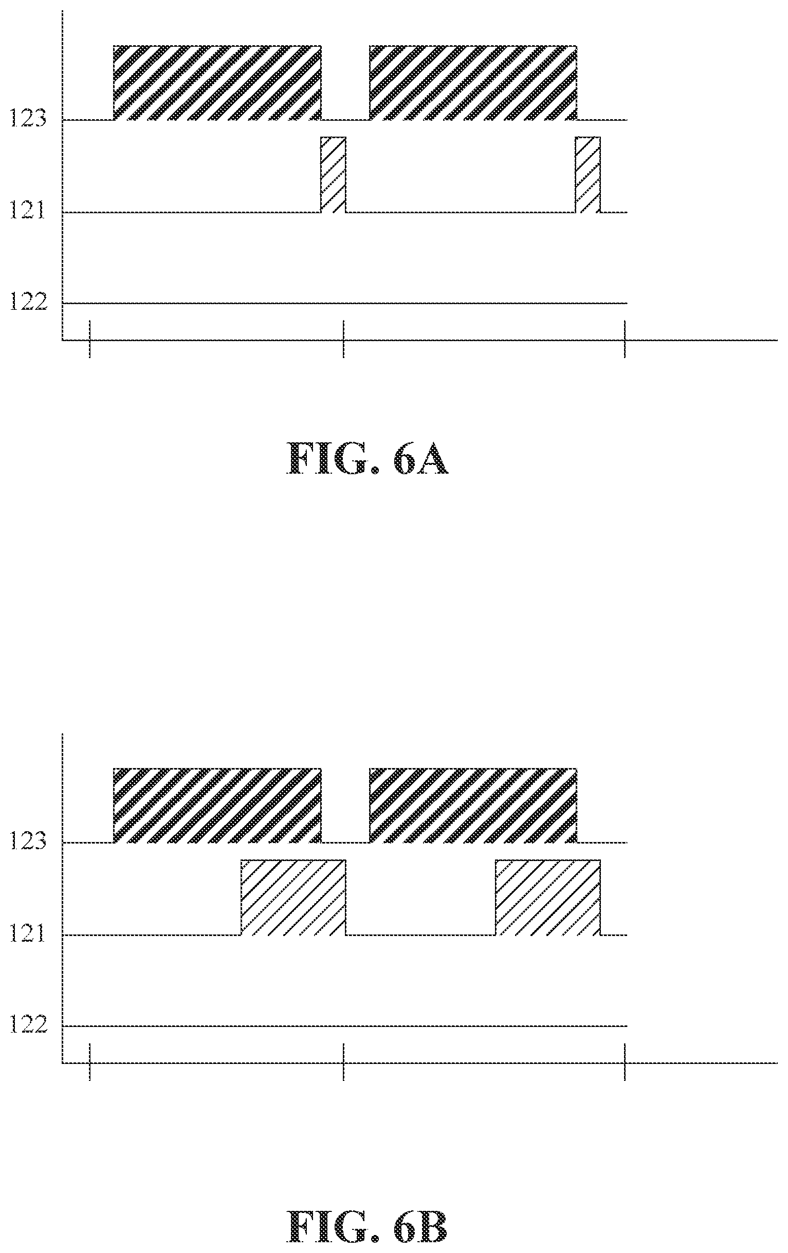
[0053] Refer to FIGS. 6A and 6B. FIG. 6A is a timing diagram illustrating the implementation of the image sensing method of the present invention; FIG. 6B is another timing diagram illustrating the implementation of the image sensing method of the present invention. Referring to Table 1 below, in some embodiments, the blue unit pixel 123 in the light-emitting state is used as the light-emitting area 31, and the red unit pixel 121 in the sensing state is used as the sensing area 32. Also, in some embodiments, referring to FIG. 6A, first, the definition step S.sub.1 is performed, and the unit pixels 12 on the display device 100 alternately emit light, wherein when a part of the unit pixels 12 emit light, defined as in a light-emitting state; when another part of the unit pixels 12 do not emit light, defined as in the sensing state. Then, the light-emitting area step S.sub.2 is executed, and the blue unit pixel 123 in the light-emitting state is used as the light-emitting area 31; followed by the sensing area step S.sub.3, wherein the red unit pixel 121 in the sensing state is used as the sensing area 32. Next, the emission step S.sub.4 is performed to drive a part of the blue unit pixels 123 in the light-emitting area 31 to emit an incident light R.sub.1 to the test object 200, and the incident light R.sub.1 is reflected by the test object 200 to generate a reflected light R.sub.2. Then, the sensing step S.sub.5 is performed to drive a portion of the red unit pixels 121 in the sensing area 32 to sense the reflected light R.sub.2, and the sensing area 32 generates a corresponding image electrical signal. Finally, the aforementioned emission step S.sub.4 and sensing step S.sub.5 are repeated.
TABLE-US-00001 TABLE 1 Drive FIG. 6A FIG. 6B Light-emitting area Blue unit pixels ON ON Sensing area Red unit pixels ON ON Green unit pixels OFF OFF
[0054] It should be further noted that, in order to avoid the interference of noise, the implementation in an ideal state is as follows: First, a part of the blue unit pixels 123 in the light-emitting area 31 are driven to emit the incident light R.sub.1 to the test object 200, Next, while turning off the light-emitting area 31, a part of the red unit pixels 121 in the sensing area 32 are driven to sense the reflected light R.sub.2. As a result, the interference of the noise, such as background light, can be effectively reduced to affect the red unit pixels 121 in the sensing area 32; however, as the thickness of the display device gradually decreases, the path of the reflected light R.sub.2 generated after the incident light R.sub.1 is emitted to the test object 200 is reduced, resulting in a significant decrease in the response time. Therefore, as shown in FIG. 6B, another embodiment according to the present invention is described as follows: First, a part of the blue unit pixels 123 in the light-emitting area 31 are driven to emit the incident light R.sub.1 to the test object 200, and the incident light R.sub.1 emitted to the test object 200 is reflected to generate a reflected light R.sub.2. When a part of the blue unit pixels 123 in the light-emitting area 31 is not turned off, a part of the red light unit pixels 121 in the sensing area 32 is driven to sense the reflected light R.sub.2, and the sensing area 32 generates a corresponding image electrical signal. However, the present invention is not limited hereto.
[0055] Accordingly, based on the display device 100 according to the present invention, and in conjunction with the image sensing method provided by the present invention, the unit pixels 12 in the light-emitting state are used as the light-emitter for under-screen fingerprint recognition, The unit pixels 12 in the sensing state are used as the sensor for under-screen fingerprint recognition, and the present invention provides a high-performance image recognition without affecting the pixels of the panel.
First Embodiment
[0056] Hereinafter, an embodiment of the first embodiment of the display device 100 of the present invention will be described with reference to the drawings.
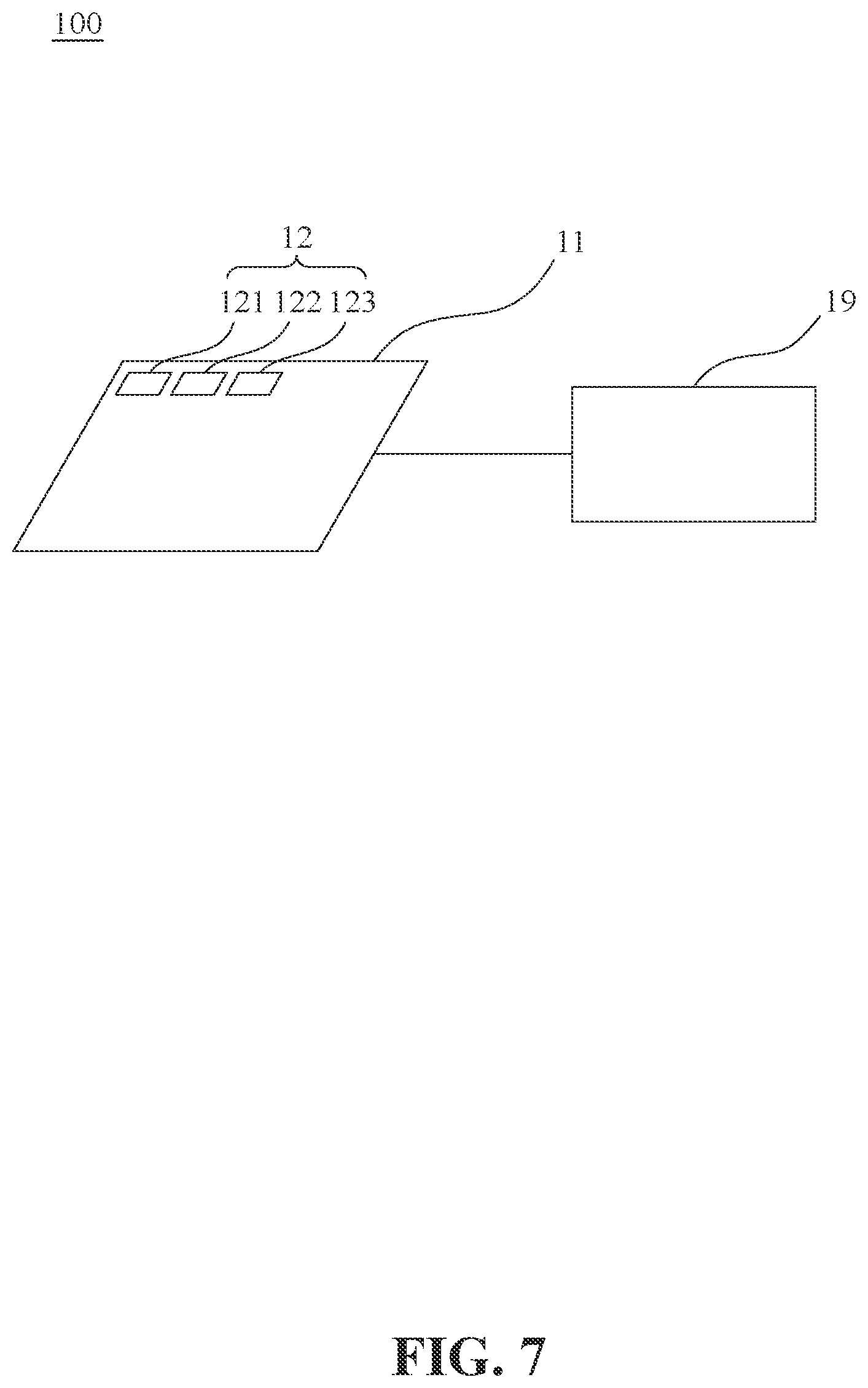
[0057] Refer to FIG. 7, which is a schematic view of a display device according to the first embodiment of the present invention. As shown in FIG. 7, the display device 100 according to the first embodiment of the present invention is applied to a fingerprint sensing system. The display device 100 includes a substrate 11, a plurality of unit pixels 12, a cover panel 13, and a readout circuit 18.
[0058] Specifically, referring to FIG. 7, the substrate 11 according to the first embodiment of the present invention has an upper surface 111 and a lower surface 112, and the unit pixels 12 are disposed between the upper surface 111 of the substrate 11 and the cover panels 13, in addition, the thickness of the cover panels 13 is about 700 microns, but the present invention is not limited hereto.
[0059] Specifically, the unit pixels 12 according to the first embodiment of the present invention include red unit pixels 121, green unit pixels 122, and blue unit pixels 123, but the present invention is not limited hereto.
[0060] It should be further explained that the display device 100 according to the first embodiment of the present invention is an organic light-emitting diode display device. The organic light-emitting diode display device can use, but is not limited to, fluorescent materials or phosphorescent materials as host material of the light-emitting layer, wherein the host material in the red unit pixel 121, the green unit pixel 122, and the blue unit pixel 123 can have different absorption spectra and light emission spectra, respectively, wherein the host material of the blue unit pixel 123 needs to absorb relatively stronger energy light to generate the light emission spectrum; the host material of the red unit pixel 121 can absorb relatively weaker energy light to generate the light emission spectrum. It can be understood that the display device 100 according to the first embodiment of the present invention can generate corresponding image electrical signals by absorbing light with energy higher than its own energy.
[0061] Specifically, the readout circuit 18 according to the first embodiment of the present invention is coupled to each of the unit pixels 12. In the present embodiment, the readout circuit 18 receives the image electrical signal and generates the corresponding image information, but the invention is not limited hereto.
[0062] Referring to FIG. 8, FIG. 8 is a flowchart illustrating the steps of performing the image sensing method according to the first embodiment of the present invention. As shown in FIG. 8, the present invention further provides an image sensing method, which can be applied to the display device 100 of the first embodiment, and the image sensing method includes the following steps:
[0063] Definition step S.sub.1': the unit pixels 12 on the display device 100 emit light alternately. When a part of the unit pixels 12 emit light, these unit pixels are defined as in a light-emitting state, and when another part of the unit pixels 12 do not emit light, these unit pixels are defined as in a sensing state; and proceed to light-emitting area step S.sub.2'.
[0064] Light-emitting area step S.sub.2': the unit pixels 12 in the light-emitting state are used as a light-emitting area 31; and proceed to sensing area step S.sub.3'.
[0065] Sensing area step S.sub.3': the unit pixels 12 in the sensing state are used as a sensing area 32; and proceed to emission step S.sub.4'.
[0066] Emission step S.sub.4': a part of the unit pixels 12 in the light-emitting area 31 emit an incident light R.sub.1 to the test object 200, and the incident light R.sub.1 emitted to the test object 200 is reflected to generate a reflected light R.sub.2, and proceed to sensing step S.sub.5'.
[0067] Sensing step S.sub.5': a part of the unit pixels 12 in the sensing area 32 sense the reflected light R.sub.2, and the sensing area 32 generates a corresponding image electrical signal, and proceed to outputting step S.sub.6'.
[0068] Output step S.sub.6': the readout circuit 18 receives the image electrical signal to generate corresponding image information.
[0069] Refer to FIGS. 9A and 9B. FIG. 9A is a timing diagram illustrating the implementation of the image sensing method of the present invention; FIG. 9B is another timing diagram illustrating the implementation of the image sensing method of the present invention. Referring to Table 2 below, in the first embodiment of the present invention, the blue unit pixel 123 in the light-emitting state is used as the light-emitting area 31, and the red unit pixel 121 and the green unit pixel 122 in the sensing state are used as the sensing area 32. For example, referring to FIG. 9A, first, the definition step S.sub.1' is performed, and the unit pixels 12 on the display device 100 alternately emit light, wherein when a part of the unit pixels 12 emit light, defined as in a light-emitting state; when another part of the unit pixels 12 do not emit light, defined as in the sensing state. Then, the light-emitting area step S.sub.2' is executed, and the blue unit pixel 123 in the light-emitting state is used as the light-emitting area 31; followed by the sensing area step S.sub.3', wherein the red unit pixel 121 and the green unit pixel 122 in the sensing state are used as the sensing area 32. Next, the emission step S.sub.4' is performed to drive a part of the blue unit pixels 123 in the light-emitting area 31 to emit an incident light R.sub.1 to the test object 200, and the incident light R.sub.1 is reflected by the test object 200 to generate a reflected light R.sub.2. Then, the sensing step S.sub.5' is performed to drive a portion of the red unit pixels 121 in the sensing area 32 to sense the reflected light R.sub.2, and the sensing area 32 generates a corresponding image electrical signal. Finally, the outputting step S.sub.6' is performed, and the readout circuit 18 receives the image electrical signal to generate a corresponding image information.
TABLE-US-00002 TABLE 2 Drive FIG. 9A FIG. 9B Light-emitting area Blue unit pixels ON ON Sensing area Red unit pixels ON ON Green unit pixels ON ON
[0070] It should be further noted that, according to the first embodiment of the present invention, the red unit pixel 121 and the green unit pixel 122 in the sensing state are used as the sensing area 32 at the same time. The reason is that different readout circuits 18 can be provided with the red unit pixel 121 the green unit pixel 122 to respectively generate corresponding image information. The multiple image information can be mutually confirmed, which further improves the accuracy of image sensing by the display device 100 according to the present invention. However, the present invention is not limited hereto.
[0071] It should be further noted that, in order to avoid the interference of noise, for the first embodiment of the present invention, the implementation in an ideal state is as follows: First, a part of the blue unit pixels 123 in the light-emitting area 31 are driven to emit the incident light R.sub.1 to the test object 200. Next, while turning off the light-emitting area 31, a part of the red unit pixels 121 and a part of green unit pixels 122 in the sensing area 32 are driven to sense the reflected light R.sub.2. As a result, the interference of the noise, such as background light, can be effectively reduced to affect the red unit pixels 121 and the green unit pixels 122 in the sensing area 32; however, as the thickness of the display device gradually decreases, the path of the reflected light R.sub.2 generated after the incident light R.sub.1 is emitted to the test object 200 is reduced, resulting in a significant decrease in the response time. Therefore, as shown in FIG. 9B, another embodiment according to the present invention is described as follows: First, a part of the blue unit pixels 123 in the light-emitting area 31 are driven to emit the incident light R.sub.1 to the test object 200, and the incident light R.sub.1 emitted to the test object 200 is reflected to generate a reflected light R.sub.2. When a part of the blue unit pixels 123 in the light-emitting area 31 is not turned off, a part of the red light unit pixels 121 and green unit pixels 122 in the sensing area 32 is driven to sense the reflected light R.sub.2, and the sensing area 32 generates a corresponding image electrical signal. However, the present invention is not limited hereto.
[0072] As such, based on the display device 100 according to the first embodiment of the present invention, and in conjunction with the image sensing method provided by the present invention, the unit pixels 12 in the light-emitting state are used as the light-emitter for under-screen fingerprint recognition, The unit pixels 12 in the sensing state are used as the sensor for under-screen fingerprint recognition, and the present invention provides a high-performance image recognition without affecting the pixels of the panel.
[0073] The following provides other examples of the display device 100, so that a person with ordinary knowledge in the technical field of the present invention can more clearly understand the possible modifications. The elements indicated by the same element symbols as in the above embodiment are substantially the same as those described above with reference to FIGS. 1 and 2. The elements, features, and advantages that are the same as those of the display device 100 will not be repeated.
[0074] Refer to FIG. 10, which is a schematic view of a display device 100 according to a second embodiment of the present invention. Compared with the first embodiment, the main structural difference of the second embodiment is that in the image sensor 100 of the second embodiment, the unit pixel 12 can be disposed on the lower surface 112 of the substrate 11. The materials and other characteristics used in the unit pixel 12 according to the second embodiment of the present invention are similar to those of the unit pixel 12 according to the first embodiment of the present invention, and will not be repeated here.
[0075] It can be understood that a person with ordinary knowledge in the technical field of the present invention can make various changes and adjustments based on the above examples, which will not be listed here.
[0076] Finally, the technical features of the present invention and its achievable technical effects are summarized as follows:
[0077] First, based on the display device 100 of the present invention, and in conjunction with the image sensing method provided by the present invention, the image successfully provides a high-performance image recognition without affecting the pixels of the panel.
[0078] Second, based on the display device 100 of the present invention, and in conjunction with the image sensing method provided by the present invention, the issue of the decreasing gap between the sub-pixels of the OLED is successfully resolved, and the difficulty for under-screen fingerprint recognition technology to use the gap between the sub-pixels of the OLED allows light to pass is overcome, and the under screen fingerprint recognition technology can still be implemented on the high-pixel OLED panel.
[0079] Third, based on the display device 100 of the present invention and in conjunction with the image sensing method provided by the present invention, the display device 100 according to the present invention not only serves as a light-emitting element, but also can be used as a sensing element for fingerprint image recognition, achieving the objectives of reducing costs and wide applicability.
[0080] Although the present invention has been described with reference to the preferred embodiments thereto, it is apparent to those skilled in the art that a variety of modifications and changes may be made without departing from the scope of the present invention which is intended to be defined by the appended claims.
* * * * *
D00000
D00001
D00002
D00003
D00004
D00005
D00006
D00007
D00008
D00009
D00010
XML
uspto.report is an independent third-party trademark research tool that is not affiliated, endorsed, or sponsored by the United States Patent and Trademark Office (USPTO) or any other governmental organization. The information provided by uspto.report is based on publicly available data at the time of writing and is intended for informational purposes only.
While we strive to provide accurate and up-to-date information, we do not guarantee the accuracy, completeness, reliability, or suitability of the information displayed on this site. The use of this site is at your own risk. Any reliance you place on such information is therefore strictly at your own risk.
All official trademark data, including owner information, should be verified by visiting the official USPTO website at www.uspto.gov. This site is not intended to replace professional legal advice and should not be used as a substitute for consulting with a legal professional who is knowledgeable about trademark law.