Optoelectronic Sensor Arrangement and Optical Measuring Method
Haiberger; Luca ; et al.
U.S. patent application number 17/425596 was filed with the patent office on 2022-03-31 for optoelectronic sensor arrangement and optical measuring method. The applicant listed for this patent is OSRAM Opto Semiconductors GmbH. Invention is credited to Luca Haiberger, Daniel Richter.
| Application Number | 20220102562 17/425596 |
| Document ID | / |
| Family ID | |
| Filed Date | 2022-03-31 |


| United States Patent Application | 20220102562 |
| Kind Code | A1 |
| Haiberger; Luca ; et al. | March 31, 2022 |
Optoelectronic Sensor Arrangement and Optical Measuring Method
Abstract
In an embodiment an optoelectronic sensor arrangement includes a carrier substrate, an illuminating device, a frequency-selective optical element and a photodetector, wherein the illuminating device and the photodetector form a stacked arrangement on or with the carrier substrate, wherein the frequency-selective optical element is arranged between the illuminating device and the photodetector, wherein the photodetector is arranged in a cavity of the carrier substrate which is covered by the illuminating device and/or the frequency-selective optical element, and wherein the frequency-selective optical element includes a divider mirror and an optical filter.
| Inventors: | Haiberger; Luca; (Regensburg, DE) ; Richter; Daniel; (Bad Abbach, DE) | ||||||||||
| Applicant: |
|
||||||||||
|---|---|---|---|---|---|---|---|---|---|---|---|
| Appl. No.: | 17/425596 | ||||||||||
| Filed: | January 29, 2020 | ||||||||||
| PCT Filed: | January 29, 2020 | ||||||||||
| PCT NO: | PCT/EP2020/052121 | ||||||||||
| 371 Date: | July 23, 2021 |
| International Class: | H01L 31/0232 20060101 H01L031/0232; H01L 31/173 20060101 H01L031/173; G02B 6/42 20060101 G02B006/42 |
Foreign Application Data
| Date | Code | Application Number |
|---|---|---|
| Feb 8, 2019 | DE | 10 2019 103 155.9 |
Claims
1.-19. (canceled)
20. An optoelectronic sensor arrangement comprising: a carrier substrate; an illuminating device; a frequency-selective optical element; and a photodetector, wherein the illuminating device and the photodetector form a stacked arrangement on or with the carrier substrate, wherein the frequency-selective optical element is arranged between the illuminating device and the photodetector, wherein the photodetector is arranged in a cavity of the carrier substrate which is covered by the illuminating device and/or the frequency-selective optical element, and wherein the frequency-selective optical element comprises a divider mirror and an optical filter.
21. The optoelectronic sensor arrangement according to claim 20, wherein the photodetector is located rearwardly of the illuminating device such that electromagnetic radiation received by the photodetector passes through the illuminating device before reaching the photodetector.
22. The optoelectronic sensor arrangement according to claim 20, wherein the frequency-selective optical element is configured to shield the photodetector from electromagnetic radiation emitted by the illuminating device.
23. The optoelectronic sensor arrangement according to claim 20, wherein the divider mirror is a Bragg mirror whose maximum reflectivity is at a wavelength corresponding to a wavelength .lamda..sub.e of a maximum of a spectral distribution of electromagnetic radiation emitted by the illuminating device.
24. The optoelectronic sensor arrangement according to claim 20, wherein the optical filter is a long-pass filter whose cut-on wavelength .lamda..sub.c is greater than a wavelength .lamda..sub.e of a maximum of a spectral distribution of electromagnetic radiation emitted by the illuminating device.
25. The optoelectronic sensor arrangement according to claim 20, wherein the illuminating device is arranged in a direction of its main radiation direction above the photodetector.
26. The optoelectronic sensor arrangement according to claim 20, wherein an overlapping direction of the stacked arrangement is oriented in a direction of a surface normal of the carrier substrate.
27. The optoelectronic sensor arrangement according to claim 20, wherein the photodetector is surrounded by the carrier substrate and/or an electromagnetic radiation-absorbing material such that radiation received by the photodetector passes exclusively through the frequency-selective optical element.
28. The optoelectronic sensor arrangement according to claim 20, wherein the illuminating device is embedded in a reflective material.
29. The optoelectronic sensor arrangement according to claim 20, wherein the illuminating device is an optoelectronic surface emitter or an optoelectronic edge emitter.
30. The optoelectronic sensor arrangement according to claim 29, wherein the illuminating device is a light-emitting diode or a laser-emitting diode.
31. The optoelectronic sensor arrangement according to claim 20, wherein the illuminating device and the photodetector are arranged on the same side of the carrier substrate.
32. The optoelectronic sensor arrangement according to claim 20, wherein the illuminating device and the photodetector are located on different sides of the carrier substrate and an optical window is arranged in the carrier substrate between the illuminating device and the photodetector.
33. The optoelectronic sensor arrangement according to claim 20, wherein the illuminating device and/or the photodetector is a flip-chip mounting element.
34. An optical measuring device comprising: a fiber-optic element optically coupled to the optoelectronic sensor arrangement according to claim 20.
35. An optical measuring method, the method comprising: coupling electromagnetic radiation generated by an illuminating device arranged on a carrier substrate into a fiber-optic element; and returning at least a portion of the radiation backscattered in the fiber-optic element to a photodetector which forms a stacked arrangement with the illuminating device on or with the carrier substrate, wherein the photodetector is located rearwardly of the illuminating device such that the electromagnetic radiation received by the photodetector passes through the illuminating device and through a frequency-selective optical element arranged between the illuminating device and the photodetector before reaching the photodetector.
36. The method according to claim 35, wherein the frequency-selective optical element exclusively transmits electromagnetic radiation which is frequency-shifted with respect to the electromagnetic radiation emitted by the illuminating device.
37. The method according to claim 35, wherein a wavelength of the backscattered radiation depends on an elongation state of the fiber-optic element.
Description
[0001] This patent application is a national phase filing under section 371 of PCT/EP2020/052121, filed Jan. 29, 2020, which claims the priority of German patent application 102019103155.9, filed Feb. 8, 2019, each of which is incorporated herein by reference in its entirety.
TECHNICAL FIELD
[0002] The present invention relates to an optoelectronic sensor arrangement, an optical measuring method, and an optical measuring device comprising an elastic fiber-optic element.
BACKGROUND
[0003] Optoelectronic sensor arrangements grouping an illuminating means, in particular an optoelectronic component such as a photodiode or a laser diode, with a photodetector on a carrier substrate in a cluster are known. For example, U.S. Pat. No. 9,836,165 B2 describes the juxtaposition of RGB illuminating means, IR emitters and optical detectors for capturing a fingerprint on a display. Further, U.S. Pat. No. 6,745,061 B1 and US Patent Application No. 2005/0107024 A1 disclose sensor arrangements that detect electromagnetic radiation reflected back from a target with a photodetector positioned adjacent to a radiation emitting unit that illuminates the target. The arrangement of the associated illuminating means and photodiodes in spatially separated substrate cavities or the use of filter components to prevent direct irradiation from the illuminating means to the photodetector result in transverse dimensions of the optoelectronic sensor arrangements that make coupling with a fiber-optic element difficult.
[0004] Furthermore, stacked optoelectronic illuminating means are known. By way of example, reference is made to U.S. Pat. No. 6,232,714 B1, which discloses a stacked arrangement with OLEDs. Further, U.S. Pat. No. 5,189,500 A describes a multilayer semiconductor device with a sensor arrangement on a first substrate side and an associated display unit on the opposite substrate side. The aforementioned semiconductor stack arrangements are not suitable for forming a small-scale optoelectronic sensor arrangement which illuminates an object and detects backscattered, frequency-shifted radiation from the object.
SUMMARY
[0005] Embodiments provide a small-size optoelectronic sensor arrangement comprising an illuminating means and a photodetector, the photodetector being configured for measuring frequency-shifted scattered light. Further embodiments provide optical measuring device comprising an elastic fiber-optic element and a coupled compact optoelectronic sensor arrangement. Other embodiments provide an optical measuring method which detects the backscattered radiation in a fiber-optic element.
[0006] Embodiments proceed from an optoelectronic sensor arrangement on a carrier substrate with an illuminating means and a photodetector. To achieve a cluster arrangement in a particularly small space, especially with regard to the transverse extension, the illuminating means and the photodetector form a stacked arrangement on or with the carrier substrate, wherein a frequency-selective optical element is arranged between the illuminating means and the photodetector. Advantageously, the photodetector is located rearwardly of the illuminating means such that the electromagnetic radiation received by the photodetector passes through the illuminating means before reaching the photodetector. Furthermore, it is preferred that the frequency-selective optical element is configured to shield the photodetector from the electromagnetic radiation emitted by the illuminating means.
[0007] The illuminating means of the optoelectronic sensor arrangement may be an optoelectronic surface emitter or an optoelectronic edge emitter forming a light emitting diode or a laser diode. A stacked arrangement of several optoelectronic components to form the illuminating means is also conceivable.
[0008] Advantageously, the illuminating means is configured for coupling into a fiber-optic element. Preferably, the illuminating means is embedded in a reflecting material, in particular in such a way that the reflecting material surrounds the illuminating means at its side walls and/or comprises a concave mirror shape, in order to intensify the radiation characteristic in the direction of the surface normal of the carrier substrate and to improve the light coupling to the fiber-optics. Preferably, the upper side of the illuminating means facing the fiber-optics remains free of the reflective material coating provided for the lateral cladding. In addition, micro-optics can be used for coupling the illuminating means and the fiber-optic element.
[0009] For the optical measurement method, the electromagnetic radiation generated by an illuminating means arranged on a carrier substrate is coupled into a fiber-optic element and at least part of the backscattered radiation in the fiber-optic element is returned to a photodetector. Thereby, the wavelength of the backscattered radiation depends in particular on the strain state of the fiber-optic element.
[0010] Preferably, the frequency-selective optical element of the stacked arrangement of the optoelectronic sensor arrangement exclusively transmits electromagnetic radiation which is frequency-shifted with respect to the electromagnetic radiation emitted by the illuminating means. Thereby, for an advantageous embodiment, the frequency-selective optical element comprises a divider mirror and/or an optical filter. The divider mirror may be a Bragg mirror whose maximum reflectivity is for a wavelength corresponding to the wavelength .lamda..sub.e of the maximum of the spectral distribution of the electromagnetic radiation emitted by the illuminating means. For an embodiment of the frequency-selective optical element with an optical filter, the latter is preferably a long pass filter whose cut-on wavelength .lamda..sub.c is greater than the wavelength .lamda..sub.e of the maximum of the spectral distribution of the electromagnetic radiation emitted by the illuminating means.
[0011] For a preferred embodiment of the optoelectronic sensor arrangement, the illuminating means is in the direction of its main radiation direction arranged above the photodetector. The overlapping direction of the stacked arrangement is oriented in the direction of the surface normal of the carrier substrate. In addition, the stacked arrangement is surrounded by the carrier substrate and/or an electromagnetic radiation-absorbing material in such a way that the radiation received by the photodetector passes exclusively through the frequency-selective optical element.
[0012] For an advantageous embodiment of the optoelectronic sensor arrangement, the illuminating means and the photodetector lie on the same side of the carrier substrate and form a stacked arrangement on the latter in combination with an intermediate frequency-selective optical element. For shielding, an arrangement of the photodetector is provided in a cavity of the carrier substrate which is covered by the illuminating means and/or the frequency-selective optical element.
[0013] For a further preferred embodiment, the illuminating means and the photodetector are positioned on different sides of the carrier substrate, whereby an optical window is arranged in the carrier substrate between the illuminating means and the photodetector, through which the scattered light to be detected reaches the photodetector. The chosen arrangement of illuminating means and photodetector simplifies the mounting, especially the contacting of the illuminating means and the photodetector in case of a design as flip-chip mounting elements.
[0014] An optical measuring device comprising a fiber-optic element, in particular an elastic fiber-optic element, and a compact optoelectronic sensor arrangement coupled thereto can be worn by a user on the body or incorporated in an article of clothing, in particular for measuring movements. In addition to the small size and the associated material savings, the optical encapsulation of the photodetector in the stacked arrangement improves the signal-to-noise ratio of the optoelectronic sensor arrangement.
BRIEF DESCRIPTION OF THE DRAWINGS
[0015] In the following, exemplary embodiments of the invention are explained in connection with figure representations. These show, in each case schematically, the following:
[0016] FIG. 1 shows a cross-sectional view of an optoelectronic sensor arrangement according to embodiments;
[0017] FIG. 2 illustrates the optical measuring method according to embodiments;
[0018] FIG. 3 shows an optical measuring device according to Embodiments,
[0019] FIG. 4 a cross-sectional view of a second embodiment of the optoelectronic sensor arrangement; and
[0020] FIG. 5 a cross-sectional view of a third embodiment of the optoelectronic sensor arrangement.
DETAILED DESCRIPTION OF ILLUSTRATIVE EMBODIMENTS
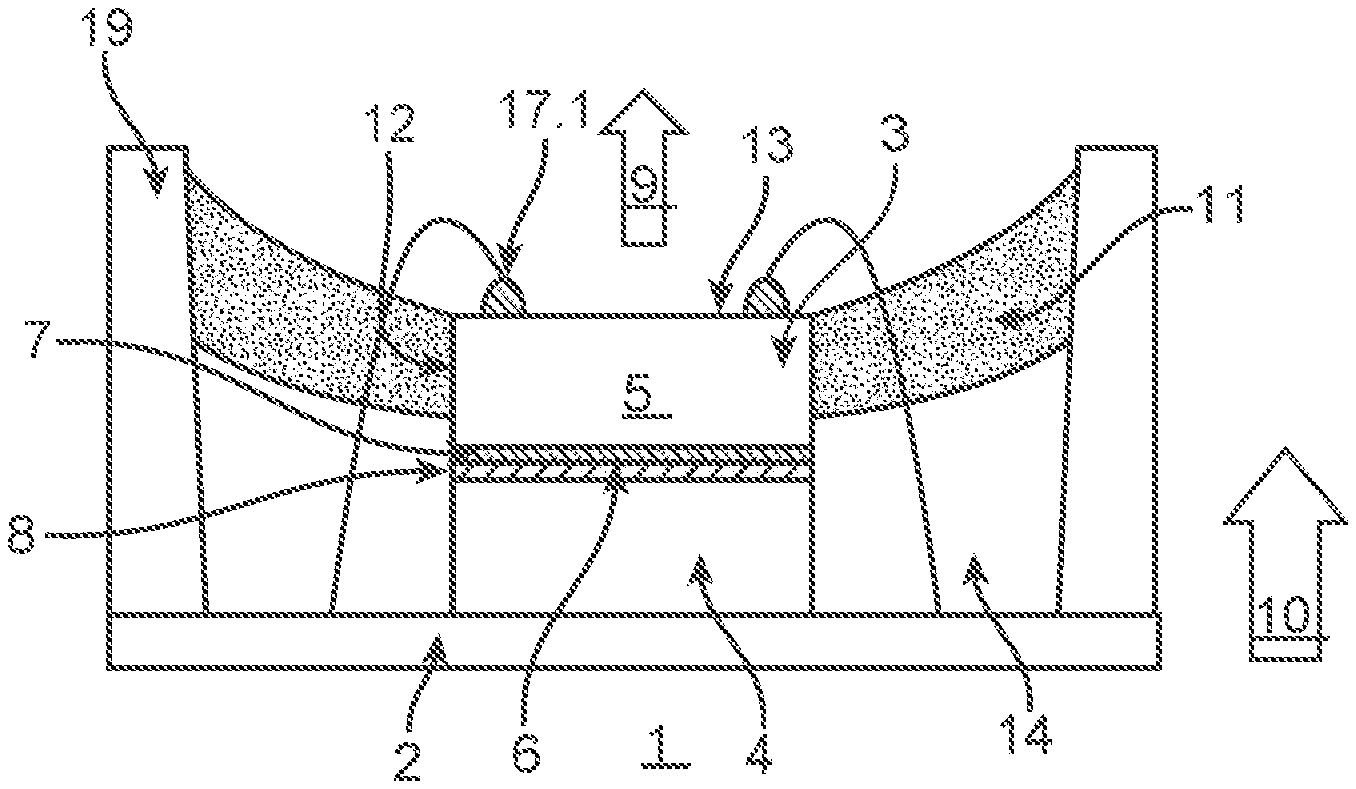
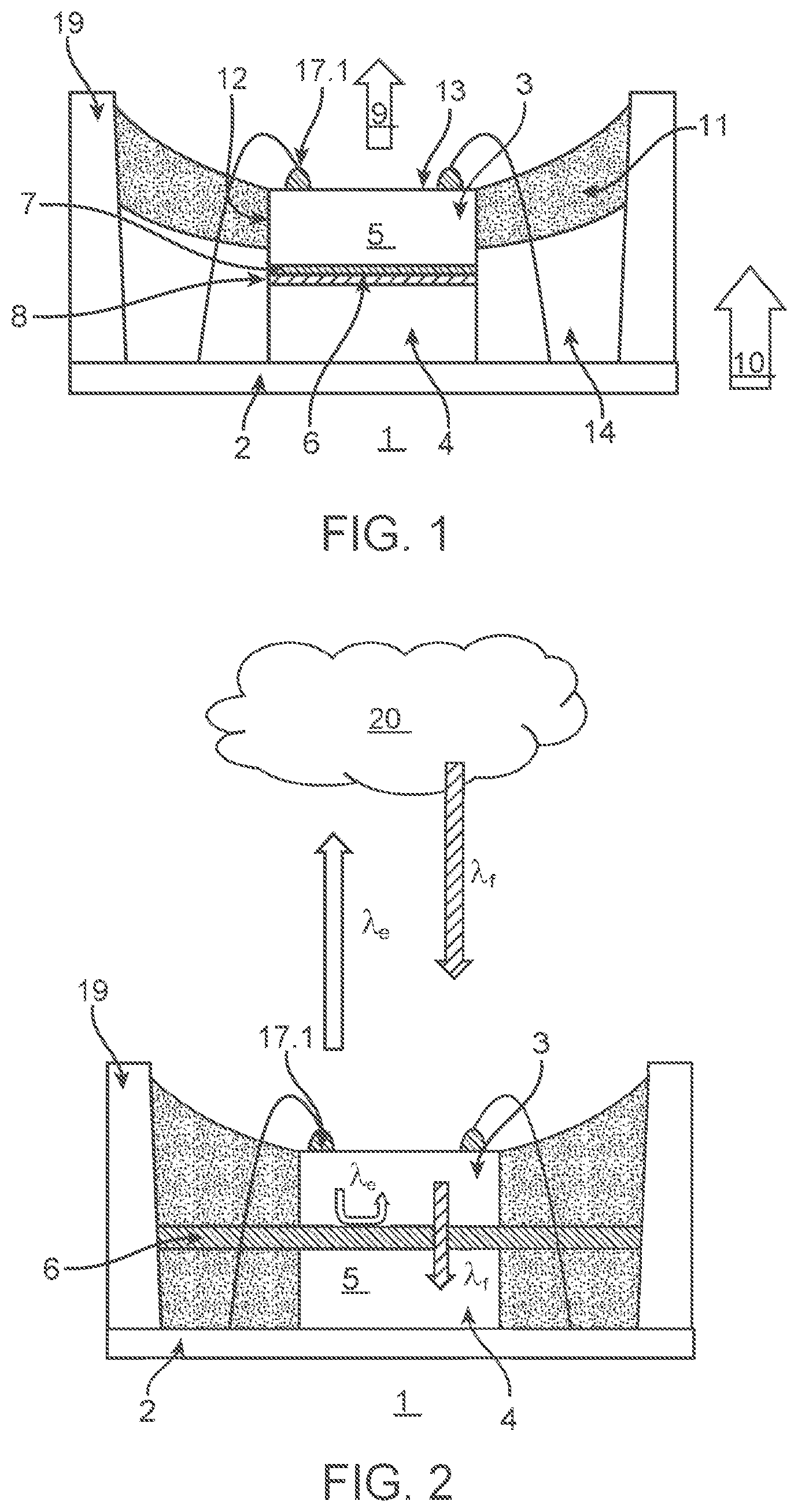
[0021] FIG. 1 represents a first embodiment of the optoelectronic sensor arrangement 1 in a schematically simplified cross-sectional view. Shown is a stacked arrangement 5 of an illuminating means 3 in the form of a light emitting diode, a frequency-selective optical element 6 and a photodiode 4 on a carrier substrate 2. The overlapping direction 10 of the stacked arrangement 5 corresponds to the direction of the surface normal of the carrier substrate 2. Here, seen in the main radiation direction 9, the illuminating means 3 lies above the frequency-selective optical element 6, which in turn is arranged above the photodiode 4.
[0022] The stacked arrangement 5 is laterally enclosed by a reflective material 11 in concave mirror form and an optical barrier 19 in such a way that electromagnetic radiation from the upper side 13 of the illuminating means 3 can take place in the main radiation direction 10. The frequency-selective optical element 6 arranged on the back side of the illuminating means 3 comprises a divider mirror 7 in the form of a Bragg mirror whose maximum reflectivity is for a wavelength corresponding to the wavelength .lamda..sub.e of the maximum of the spectral distribution of the electromagnetic radiation emitted by the illuminating means 3. The further part of the frequency-selective optical element 6 is formed by an optical filter 8 arranged under the divider mirror 7, which is designed as a long-pass filter whose cut-on wavelength .lamda..sub.c is greater than the wavelength .lamda..sub.e of the maximum of the spectral distribution of the electromagnetic radiation emitted by the illuminating means 3.
[0023] The photodetector 4 is enclosed by a layer of electromagnetic radiation-absorbing material 11 and the opaque carrier substrate 2 in such a way that the radiation to be detected reaches the photodetector 4 exclusively through the frequency-selective optical element 6 of the stacked arrangement 5. In this way, the measuring method illustrated in FIG. 2 can be realized.
[0024] The illumination of a measuring object 20 by the illuminating means 3 is shown with a spectral distribution whose maximum lies at a wavelength of .lamda..sub.e. At least a portion of the light backscattered by the measuring object 20 comprises a wavelength of .lamda..sub.f which is frequency shifted with respect to the wavelength .lamda..sub.e, wherein .lamda..sub.f>.lamda..sub.e is assumed. By choosing the cut-on wavelength .lamda..sub.c of the optical filter 8 to be .lamda..sub.f>.lamda..sub.c>.lamda..sub.e, only the light backscattered from the measuring object 20 reaches the photodetector 4. If the optical measuring device shown schematically simplified in FIG. 3 is used for the measurement with a fiber-optic element 16 to which an optoelectronic sensor arrangement 1 is optically coupled, the frequency shift of the backscattered radiation with wavelength .lamda..sub.f depends on the strain state of the fiber-optic element 16, which can be determined by the signal at the photodetector 4.
[0025] FIG. 4 shows a schematically simplified cross-sectional view of a second embodiment of the optoelectronic sensor arrangement 1. The same reference signs are used for the components corresponding to the first embodiment. The arrangement of the photodetector 4 in a cavity of the carrier substrate 2 is shown, which is covered by the divider mirror 7 of the frequency-selective element 6 and the illuminating means 3 in such a way that all the radiation incident on the photodetector 4 must pass through the illuminating means 3 and the frequency-selective optical element 6.
[0026] The contacting 17.2 of the illuminating means 3 is from the back side, so that a flip-chip mounting element can be used. Accordingly, the photodetector 4 can be formed by a flip-chip mounting element if, as shown in FIG. 4, the contacting 17.3 from the carrier substrate back side is realized by a via connection in the bottom of the cavity.
[0027] FIG. 5 shows a schematically simplified cross-sectional view of a third embodiment of the optoelectronic sensor arrangement 1. This has an arrangement of the illuminating means 3 on a first side of the carrier substrate 2, while the photodetector 4 is placed on the opposite substrate side. Accordingly, the carrier substrate 2 is additionally part of the stacked arrangement 5, which comprises the illuminating means 3, the frequency-selective optical element 6 and the photodetector 4. In this case, the photodetector 4 is surrounded by an opaque component made of an electromagnetic radiation-absorbing material 14 and radiation can only enter the measuring area through an optical window 15 in the carrier substrate 2, which is covered by the illuminating means 3 and the frequency-selective optical element 6. For the shown embodiment, the illuminating means 3 and the photodetector 4 can advantageously be realized by flip-chip mounting elements, the contacts 17.4 and 17.5 of which originate from the respective assigned side of the carrier substrate 2.
[0028] Although the invention has been illustrated and described in detail by means of the preferred embodiment examples, the present invention is not restricted by the disclosed examples and other variations may be derived by the skilled person without exceeding the scope of protection of the invention.
* * * * *
D00000
D00001
D00002
D00003
XML
uspto.report is an independent third-party trademark research tool that is not affiliated, endorsed, or sponsored by the United States Patent and Trademark Office (USPTO) or any other governmental organization. The information provided by uspto.report is based on publicly available data at the time of writing and is intended for informational purposes only.
While we strive to provide accurate and up-to-date information, we do not guarantee the accuracy, completeness, reliability, or suitability of the information displayed on this site. The use of this site is at your own risk. Any reliance you place on such information is therefore strictly at your own risk.
All official trademark data, including owner information, should be verified by visiting the official USPTO website at www.uspto.gov. This site is not intended to replace professional legal advice and should not be used as a substitute for consulting with a legal professional who is knowledgeable about trademark law.