Active Matrix Organic Light-emitting Diode Display Device And Method Of Manufacturing The Same
AHN; Jong Hyun ; et al.
U.S. patent application number 16/641965 was filed with the patent office on 2021-05-20 for active matrix organic light-emitting diode display device and method of manufacturing the same. The applicant listed for this patent is INDUSTRY-ACADEMIC COOPERATION FOUNDATION, YONSEI UNIVERSITY. Invention is credited to Jong Hyun AHN, Sa Rang BAE, Min Woo CHOI, Soo Young KIM, Yong Ju PARK, Bhupendra Kumar SHARMA.
| Application Number | 20210151537 16/641965 |
| Document ID | / |
| Family ID | 1000005413708 |
| Filed Date | 2021-05-20 |


View All Diagrams
| United States Patent Application | 20210151537 |
| Kind Code | A1 |
| AHN; Jong Hyun ; et al. | May 20, 2021 |
ACTIVE MATRIX ORGANIC LIGHT-EMITTING DIODE DISPLAY DEVICE AND METHOD OF MANUFACTURING THE SAME
Abstract
The present disclosure discloses an active matrix organic light-emitting diode display device and a manufacturing method thereof. The method includes forming a sacrificial layer on a carrier layer; forming a flexible substrate on the sacrificial layer; forming a first insulating layer on the flexible substrate; forming at least one transition metal chalcogenide based backplane on the first insulating layer; and forming an opening unit after forming a capping layer on the at least one transition metal chalcogenide based backplane; and forming at least one active matrix organic light-emitting diode unit which is electrically connected to the at least one transition metal chalcogenide based backplane in the opening unit.
| Inventors: | AHN; Jong Hyun; (Seoul, KR) ; KIM; Soo Young; (Seoul, KR) ; CHOI; Min Woo; (Seoul, KR) ; PARK; Yong Ju; (Seoul, KR) ; SHARMA; Bhupendra Kumar; (Seoul, KR) ; BAE; Sa Rang; (Seoul, KR) | ||||||||||
| Applicant: |
|
||||||||||
|---|---|---|---|---|---|---|---|---|---|---|---|
| Family ID: | 1000005413708 | ||||||||||
| Appl. No.: | 16/641965 | ||||||||||
| Filed: | April 22, 2019 | ||||||||||
| PCT Filed: | April 22, 2019 | ||||||||||
| PCT NO: | PCT/KR2019/004822 | ||||||||||
| 371 Date: | February 25, 2020 |
| Current U.S. Class: | 1/1 |
| Current CPC Class: | H01L 2227/323 20130101; H01L 27/3248 20130101; H01L 51/0097 20130101; H01L 27/1225 20130101; H01L 2227/326 20130101; H01L 2251/5338 20130101; H01L 51/56 20130101; H01L 27/3262 20130101 |
| International Class: | H01L 27/32 20060101 H01L027/32; H01L 51/00 20060101 H01L051/00; H01L 51/56 20060101 H01L051/56 |
Foreign Application Data
| Date | Code | Application Number |
|---|---|---|
| Oct 2, 2018 | KR | 10-2018-0117746 |
Claims
1. A manufacturing method of an active matrix organic light-emitting diode display device, comprising: forming a sacrificial layer on a carrier layer; forming a flexible substrate on the sacrificial layer; forming a first insulating layer on the flexible substrate; forming at least one transition metal chalcogenide based backplane on the first insulating layer; forming an opening unit after forming a capping layer on the at least one transition metal chalcogenide based backplane; and forming at least one active matrix organic light-emitting diode unit which is electrically connected to the at least one transition metal chalcogenide based backplane in the opening unit, wherein the forming of at least one transition metal chalcogenide based backplane includes: forming a first insulating layer on the flexible substrate; forming source/drain electrodes which are spaced apart from each other on the first insulating layer; forming a channel layer including transition metal chalcogenide in a channel region and the source/drain electrodes of the flexible substrate; doping the channel layer by forming a second insulating layer on the channel layer; and forming a gate electrode on the second insulation layer, and in the at least one transition metal chalcogenide based backplane, the channel region is doped with electrons by the doping and a contact portion of the source/drain electrodes with the channel layer is doped with electrons.
2. The manufacturing method according to claim 1, further comprising: removing the sacrificial layer and the carrier layer.
3. The manufacturing method according to claim 1, wherein the active matrix organic light-emitting diode unit further includes: forming a first electrode which is electrically connected to the at least one transition metal chalcogenide based backplane; forming an organic light emitting layer on the first electrode; and forming a second electrode on the organic light emitting layer.
4. The manufacturing method according to claim 3, wherein the organic light emitting layer includes a hole injection layer, a hole transporting layer, a light emitting layer, an electron transporting layer, and an electron injection layer.
5. The manufacturing method according to claim 3, wherein the first electrode is a transparent electrode.
6. The manufacturing method according to claim 1, wherein the transition metal chalcogenide is a single layer or a multilayered structure.
7. The manufacturing method according to claim 1, wherein the first insulating layer and the second insulating layer are formed of the same material.
8. The manufacturing method according to claim 1, wherein the channel layer is any one of a single layer, a double layer, and a multiple layer.
9. The manufacturing method according to claim 1, wherein the first insulating layer or the second insulating layer is any one of alumina (Al.sub.2O.sub.3), silica (SiO.sub.2), hafnium oxide (HfO.sub.2), zirconium oxide (ZrO.sub.2), zinc oxide (ZnO)m and titanium oxide (TiO.sub.2).
10. An active matrix organic light-emitting diode display device manufactured by the method according to claim 1.
Description
CROSS-REFERENCE TO RELATED APPLICATIONS
[0001] This application claims priority to and the benefit of Korean Patent Application No. 10-2018-0117746 filed in the Korean Intellectual Property Office on Oct. 2, 2018, the entire contents of which are incorporated herein by reference.
TECHNICAL FIELD
[0002] The present disclosure relates to an active matrix organic light-emitting diode display device and a method of manufacturing the same, and more particularly, to an active matrix organic light-emitting diode display device which includes a transition metal chalcogenide based backplane including a channel layer interposed between dielectric layers having a high permittivity to improve electron mobility and reduce both a channel resistance and a contact resistance and a method of manufacturing the same. This research relates to the center for strain engineered electronic devices in the leader researcher support project (No. 2017-11-1578).
BACKGROUND ART
[0003] Transition metal chalcogenides (TMDs) which are classified as two-dimensional materials show excellent physical properties required for devices according to a next generation of electronic or optoelectronics. The transition metal chalcogenides have a multilayered structure and are bonded by the interlayer van der Waals force, so that it is easy to mechanically peel off the transition metal chalcogenides through an adhesive or the like.
[0004] The transition metal chalcogenides have been reported to be superior to the existing material because of electrical and mechanical characteristics and are utilized for a large capacity of flexible switching based application based on the material characteristics.
[0005] Specifically, since the transition metal chalcogenides provide advantages to switch an organic light-emitting diode on a flexible substrate, such as a high carrier mobility, a high light transmittance, and a low bending stiffness, as compared with an inorganic semiconductor of the related art, a backplane for a flexible organic light-emitting diode (flexible OLED) display is known as one of the most promising applications of the transition metal chalcogenides.
[0006] When the transition metal chalcogenides are manufactured by a mechanical peeling method, only pieces having a very small area can be formed so that there is a limit to implement large-area electronic devices. Therefore, studies for high quality and large area synthesis are actively being performed to overcome the above-mentioned disadvantages.
[0007] Therefore, a method of synthesizing the transition metal chalcogenides to have a large size corresponding to a wafer size using chemical vapor deposition has been used among synthesizing methods of transition metal chalcogenides.
[0008] However, the transition metal chalcogenides grown using the chemical vapor deposition have a difficulty to be applied to a backplane for a flexible system or a large area organic light-emitting diode display due to a low mobility and an inferior semiconductor characteristic caused by a small crystal grain boundary.
SUMMARY OF THE INVENTION
[0009] An object of the present disclosure is to provide an active matrix organic light-emitting diode display device which includes a transition metal chalcogenide based backplane with an increased electron mobility of a backplane by interposing a transition metal chalcogenide based channel layer between insulating layers having a high permittivity and a method of manufacturing the same.
[0010] Another object of the present disclosure is to provide an active matrix organic light-emitting diode display device including a transition metal chalcogenide based backplane which forms an insulating layer having a high dielectric constant above a transition metal chalcogenide based channel layer to be doped with a channel layer of the back plane to simultaneously lower a channel resistance and a contact resistance and a method of manufacturing the same.
[0011] Another object of the present disclosure is to provide an active matrix organic light-emitting diode display device including a transition metal chalcogenide based backplane which forms an insulating layer having a high permittivity below a transition metal chalcogenide based channel layer to reduce a roughness of a substrate or a scattering effect due to charges trapped by the substrate, thereby effectively reducing hysteresis and a method of manufacturing the same.
[0012] Another object of the present disclosure is to provide an active matrix organic light-emitting diode display device which is applicable to a wearable device or a flexible device to be utilized in various fields including medical or sports, such as health monitoring system which is attachable to skin or clothes through a transition metal chalcogenide based backplane having excellent reliability and uniformity and a method of manufacturing the same.
[0013] Another object of the present disclosure is to provide an active matrix organic light-emitting diode display device and a method of manufacturing the same which are capable of manufacturing a large size tactile sensor using a transition metal chalcogenide based backplane.
[0014] According to an aspect of the present disclosure, a manufacturing method of an active matrix organic light-emitting diode display device includes forming a sacrificial layer on a carrier layer, forming a flexible substrate on the sacrificial layer; forming a first insulating layer on the flexible substrate; forming at least one transition metal chalcogenide based backplane on the first insulating layer; and forming an opening unit after forming a capping layer on the at least one transition metal chalcogenide based backplane; and forming at least one active matrix organic light-emitting diode unit which is electrically connected to the at least one transition metal chalcogenide based backplane in the opening unit, in which the forming of at least one transition metal chalcogenide based backplane includes: forming a first insulating layer on the flexible substrate; forming source/drain electrodes which are spaced apart from each other on the first insulating layer; forming a channel layer including transition metal chalcogenide in a channel region and the source/drain electrodes of the flexible substrate; doping the channel layer by forming a second insulating layer on the channel layer; and forming a gate electrode on the second insulation layer, and in the at least one transition metal chalcogenide based backplane, the channel region is doped with electrons by the doping and a contact portion of the source/drain electrodes with the channel layer is doped with electrons.
[0015] The manufacturing method of an active matrix organic light emitting diode display device may further include: removing the sacrificial layer and the carrier layer. The active matrix organic-light emitting diode unit may further include: forming a first electrode which is electrically connected to the at least one transition metal chalcogenide based backplane; forming an organic light emitting layer on the first electrode; and forming a second electrode on the organic light emitting layer.
[0016] The organic light emitting layer may include a hole injection layer, a hole transporting layer, a light emitting layer, an electron transporting layer, and an electron injection layer.
[0017] The first electrode may be a transparent electrode.
[0018] The transition metal chalcogenide may be a single layer or a multilayered structure.
[0019] The first insulating layer and the second insulating layer may be formed of the same material.
[0020] The channel layer may be any one of a single layer, a double layer, and a multiple layer.
[0021] The first insulating layer or the second insulating layer may be any one of alumina (Al.sub.2O.sub.3), silica (SiO.sub.2), hafnium oxide (HfO.sub.2), zirconium oxide (ZrO.sub.2), zinc oxide (ZnO) and titanium oxide (TiO.sub.2).
[0022] According to another aspect of the present disclosure, an active matrix organic light-emitting diode display device is manufactured by a method according to any one of claims 1 to 10.
[0023] An object of the present disclosure is to provide an active matrix organic light-emitting diode display device which includes a transition metal chalcogenide based backplane with an increased electron mobility of a backplane by interposing a transition metal chalcogenide based channel layer between insulating layers having a high permittivity and a method of manufacturing the same.
[0024] The present disclosure may provide an active matrix organic light-emitting diode display device including a transition metal chalcogenide based backplane which forms an insulating layer having a high permittivity above a transition metal chalcogenide based channel layer to be doped with a channel layer of the back plane to simultaneously reduce a channel resistance and a contact resistance and a method of manufacturing the same.
[0025] The present disclosure may provide an active matrix organic light-emitting diode display device including a transition metal chalcogenide based backplane which forms an insulating layer having a high permittivity below a transition metal chalcogenide based channel layer to reduce a roughness of a substrate or a scattering effect due to charges trapped by the substrate, thereby effectively reducing hysteresis and a method of manufacturing the same.
[0026] The present disclosure may provide an active matrix organic light-emitting diode display device which is applicable to a wearable device or a flexible device to be utilized in various fields including medical or sports, such as health monitoring system which is attachable to skin or clothes through a transition metal chalcogenide based back plane having an excellent reliability and uniformity and a method of manufacturing the same.
[0027] The present disclosure may provide an active matrix organic light-emitting diode display device which enables a large area tactile sensor using a transition metal chalcogenide based backplane and a method of manufacturing the same.
BRIEF DESCRIPTION OF THE DRAWINGS
[0028] FIGS. 1A to 1J illustrate a manufacturing method of an active matrix organic light-emitting diode display device according to an embodiment of the present disclosure.
[0029] FIGS. 2A to 2F illustrate a manufacturing method of a transition metal chalcogenide based backplane 200 included in an active matrix organic light-emitting diode display device 100 according to an embodiment of the present disclosure.
[0030] FIG. 3A illustrates a three-dimensional structure of a molybdenum disulfide based backplane formed by a manufacturing method of a transition metal chalcogenide based backplane according to an embodiment of the present disclosure.
[0031] FIG. 3B illustrates an optical image of an active matrix organic light-emitting diode display device formed on a flexible substrate and an image when an wearable display to which an active matrix organic light-emitting diode display device is applied is attached to a wrist.
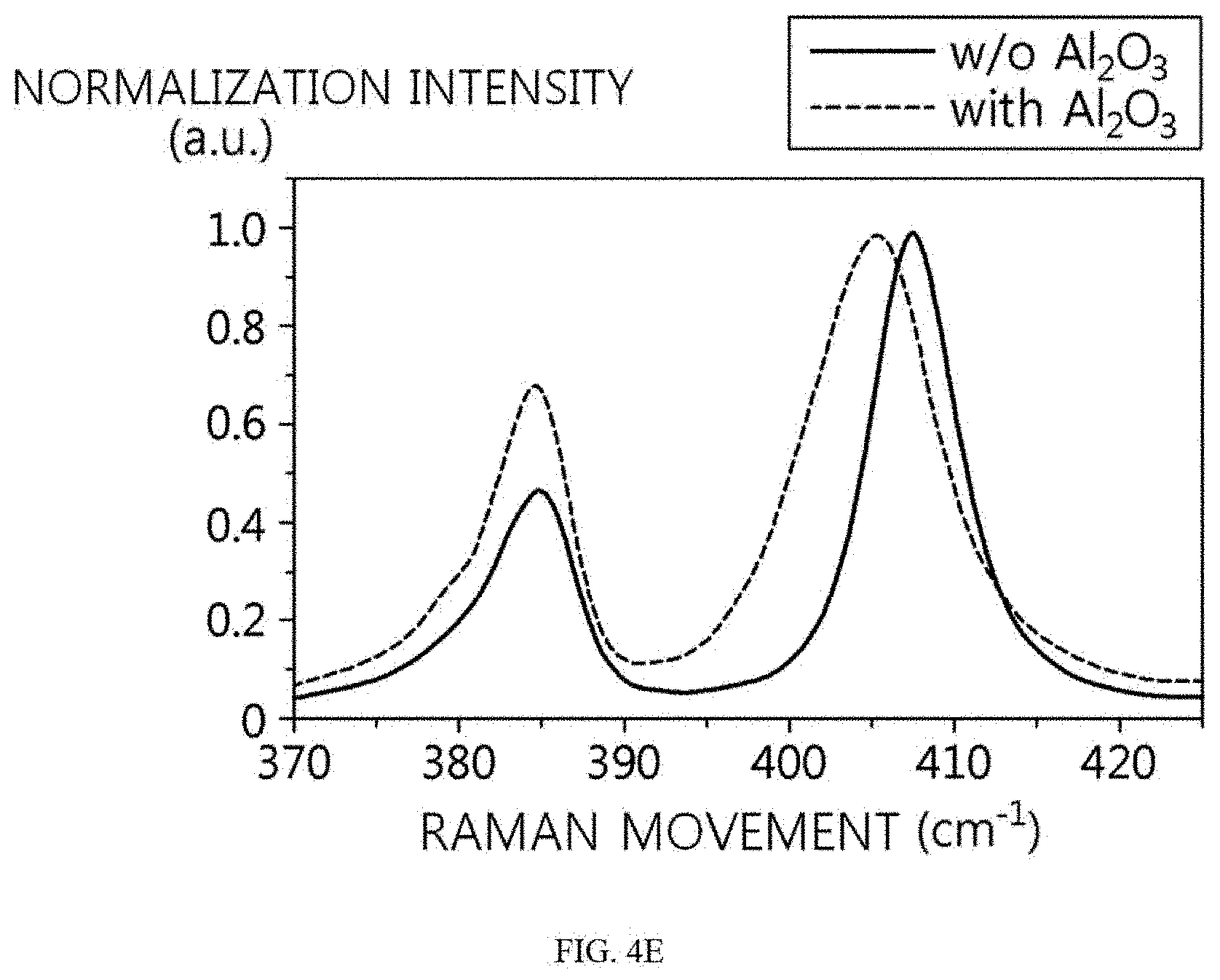
[0032] FIGS. 4A to 4F illustrate a Raman spectrum and a photoluminescence spectrum of a channel layer in accordance with a position of an Al.sub.2O.sub.3 layer in a molybdenum disulfide based backplane formed by a manufacturing method of a transition metal chalcogenide based backplane according to an embodiment of the present disclosure.
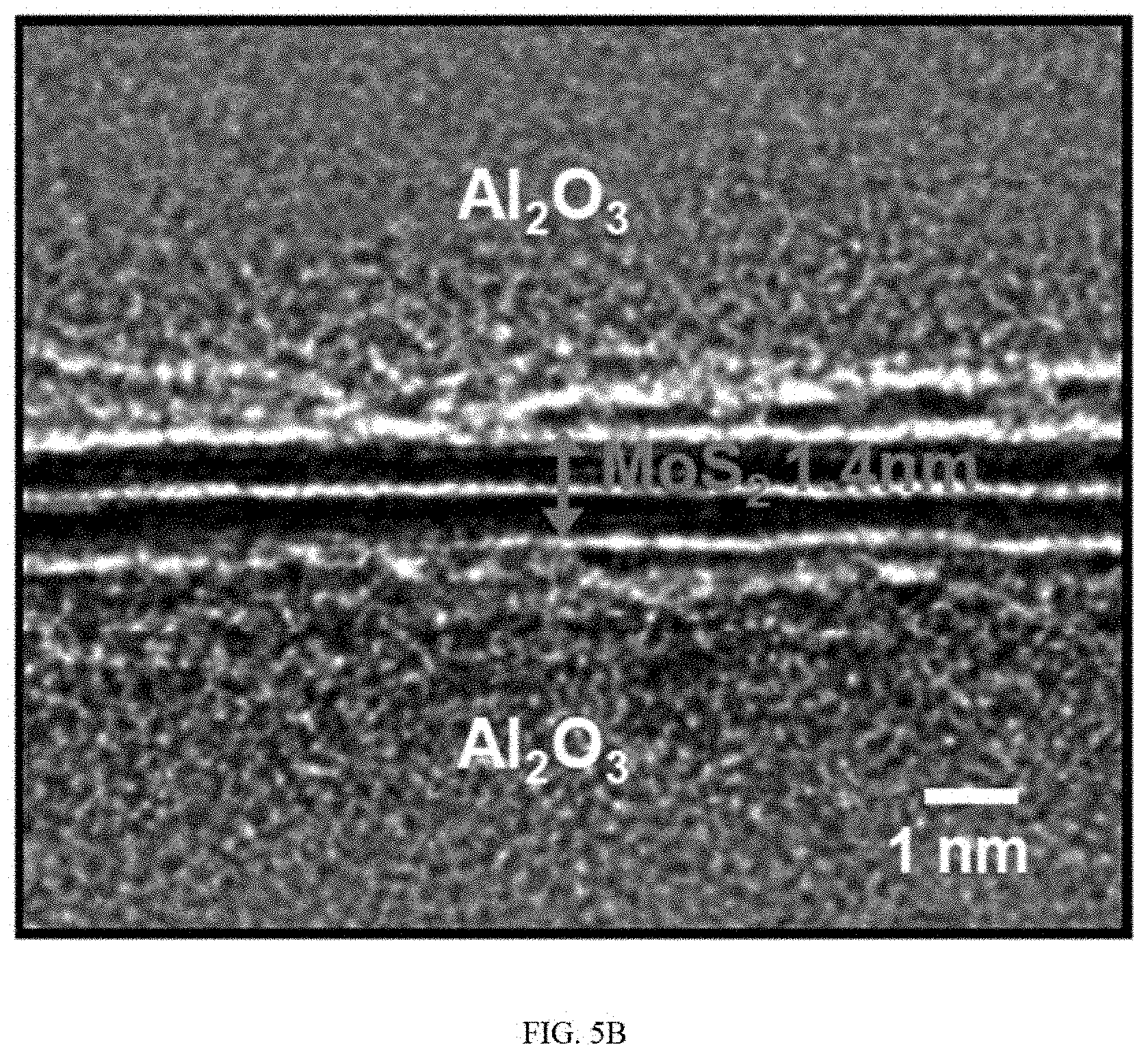
[0033] FIG. 5A illustrates an atomic force microscope of an SiO.sub.2 substrate and an SiO.sub.2 substrate on which an Al.sub.2O.sub.3 layer is deposited, in a molybdenum disulfide based backplane formed by a manufacturing method of a transition metal chalcogenide based backplane according to an embodiment of the present disclosure. FIG. SB illustrates a cross-sectional transmission electron microscopy image of a structure in which a channel layer is interposed between Al.sub.2O.sub.3 layers.
[0034] FIG. 6 illustrates that a channel area and a contact resistance are reduced by an Al.sub.2O.sub.3 layer in a molybdenum disulfide based backplane formed by a manufacturing method of a transition metal chalcogenide based backplane according to an embodiment of the present disclosure.
[0035] FIG. 7A is a graph illustrating a switching characteristic of a molybdenum disulfide based backplane formed by a manufacturing method of a transition metal chalcogenide based backplane according to an embodiment of the present disclosure and a molybdenum disulfide based backplane having various structures. FIG. 7B is a graph illustrating an output characteristic. FIG. 7C is a graph illustrating a mobility.
[0036] FIG. 8 is a graph illustrating a hysteresis curve of a molybdenum disulfide based backplane formed by a manufacturing method of a transition metal chalcogenide based backplane according to an embodiment of the present disclosure and a molybdenum disulfide based backplane on which an Al.sub.2O.sub.3 layer is not deposited.
[0037] FIG. 9A is a view illustrating an electrical characteristic of a single crystal molybdenum disulfide based backplane on which an Al.sub.2O.sub.3 layer is not deposited. FIG. 9B is a view illustrating an electrical characteristic of a single crystal molybdenum disulfide based backplane on which a channel layer is interposed between Al.sub.2O.sub.3 layers.
[0038] FIGS. 10A to 10C are graphs illustrating a result of analyzing a contact resistance and a channel resistance of a molybdenum disulfide based backplane formed by a manufacturing method of a transition metal chalcogenide based backplane according to an embodiment of the present disclosure in accordance with a transfer length method (TLM).
[0039] FIG. 11A is a graph illustrating an electrical characteristic of a molybdenum disulfide based backplane formed by a manufacturing method of a transition metal chalcogenide based backplane according to an embodiment of the present disclosure. FIG. 11B illustrates a histogram.
[0040] FIGS. 12A and 12B are graphs illustrating a stability of a molybdenum disulfide based backplane formed by a manufacturing method of a transition metal chalcogenide based backplane according to an embodiment of the present disclosure.
[0041] FIGS. 13A to 13E illustrate a performance of a single pixel of an active matrix organic light-emitting diode which is electrically connected to a molybdenum disulfide based backplane formed by a manufacturing method of a transition metal chalcogenide based backplane according to an embodiment of the present disclosure.
[0042] FIG. 14A illustrates an image when an active matrix organic light-emitting diode display device according to an embodiment of the present disclosure is attached to a wrist of a human.
[0043] FIG. 14B illustrates a current mapping result during an operation of an active matrix organic light-emitting diode display device.
[0044] FIG. 15A illustrates an optical image of a process of separating an active matrix organic light-emitting diode display device according to an embodiment of the present disclosure from a carrier substrate. FIG. 15B is a graph illustrating a repeated bending test result with a bending radius of 0.7 mm.
[0045] FIG. 16A illustrates a structure of an active tactile sensor including a transition metal chalcogenide based backplane according to an embodiment of the present disclosure. FIG. 16B illustrates an optical image of an active tactile sensor.
[0046] FIG. 17A is a graph illustrating a current-voltage characteristic of an active tactile sensor according to an embodiment of the present disclosure. FIG. 17B is a graph illustrating a resistance change in accordance with a time. FIG. 17C is a graph illustrating a repetitive characteristic in accordance with a pressure.
[0047] FIGS. 18A to 18D are graphs illustrating a flexible characteristic of an active tactile sensor according to an embodiment of the present disclosure.
[0048] FIG. 19A is a graph illustrating a low crosstalk characteristic of an active tactile sensor according to an embodiment of the present disclosure.
[0049] FIG. 19B is a graph illustrating a resistance change of an active tactile sensor.
[0050] FIG. 19C is an image illustrating pressure mapping when letters are input on an active tactile sensor.
[0051] FIG. 20 illustrates a resistance change when an active tactile sensor is bonded onto a palm and then a light object is held in an active tactile sensor according to an embodiment of the present disclosure.
DETAILED DESCRIPTION OF THE EMBODIMENT
[0052] Hereinafter, exemplary embodiments of the present invention will be described in detail with reference to accompanying drawings and contents described in the accompanying drawings, but the present invention is not limited or restricted by the exemplary embodiments.
[0053] The terms used in the present specification are for explaining the embodiments rather than limiting the present invention. Unless particularly stated otherwise in the present specification, a singular form also includes a plural form. The word "comprises" and/or "comprising" used in the present specification will be understood to imply the inclusion of stated constituents, steps, operations and/or elements but not the exclusion of any other constituents, steps, operations and/or elements.
[0054] It may not be interpreted that arbitrary aspect or design of exemplary embodiments", "example", "aspect", or "instance" used in this specification is better than other aspects or designs or has an advantage.
[0055] Further, the term "or" means "inclusive or" rather than "exclusive or". That is, unless stated otherwise or clearly understood from the context, the expression "x uses a or b" means any one of natural inclusive permutations.
[0056] Further, a singular form ("a" or "an") used in the specification and the claims should be interpreted as "one or more" unless mentioned otherwise or clearly understood to indicate a singular form from the context.
[0057] Further, when it is described that a part such as a film, a layer, a region, or a component is disposed "on" or "above" the other part, it is not only immediately on the other part, but also a third film, layer, a region, or a component is interposed between the above two parts.
[0058] Those skilled in the art may make various modifications to the present invention and the present invention may have various embodiments thereof, and thus specific embodiments will be illustrated in the drawings and described in detail in detailed description. However it should be understood that the invention is not limited to the specific embodiments, but includes all changes, equivalents, or alternatives which are included in the spirit and technical scope of the present invention. In the description of respective drawings, like reference numerals denote like elements.
[0059] FIGS. 1A to 1J illustrate a manufacturing method of an active matrix organic light-emitting diode display device according to an embodiment of the present disclosure.
[0060] Referring to FIG. 1A, according to a manufacturing method of an active matrix organic light-emitting diode display device 100 according to an embodiment of the present disclosure, a flexible substrate 130 is formed on a carrier layer 110 on which a sacrificial layer 120 is formed.
[0061] The carrier layer 100 is necessary to maintain a shape and uses a silicon wafer (Si wafer) which has no defect at a high purity and has an excellent electrical property. Depending on the embodiment, the carrier layer 110 may be a glass substrate as an insulating substrate, but is not limited thereto, and may be formed of various materials.
[0062] The sacrificial layer 120 is a member which separates the carrier layer 100 from the flexible substrate 130 in a process to be performed later and a material thereof is not specifically limited.
[0063] For example, the material of the sacrificial layer may include at least one selected from a group consisting of polyethylene, polypropylene, polydimethylsiloxane (PDMS), poly(methylmethacrylate) (PMMA), polyimide, polycarbonate, polyacrilate, polyetherimide, polyethersulfone, polyethylene terphthalate, polyethylene naphthalate, polysulfone, polyvinylidene fluoride, and polyacrylonitrile.
[0064] The flexible substrate 130 is a substrate which supports various components of a transition metal chalcogenide based backplane and an active organic light-emitting oxide diode unit and a material thereof is not specifically limited.
[0065] For example, the flexible substrate 130 may be formed of any one material selected from a group consisting of glass, polyimide polymer, polyester polymer, silicon polymer, acrylic polymer, polyolefin polymer, or a copolymer thereof.
[0066] Depending on the embodiment, the flexible substrate 130 may be formed of a transparent flexible material configured by any one material selected from a group consisting of polyester, polyvinyl, polycarbonate, polyethylene, polyacetate, polyimide, polyethersulphone (PES), polyacrylate (PAR), polyethylenenaphthelate (PEN), and polyethyleneterephehalate (PET).
[0067] Referring to FIG. 1B, according to the manufacturing method of an active matrix organic light-emitting diode display device 100 according to an embodiment of the present disclosure, a first insulating layer 140 is formed on the flexible substrate 130.
[0068] The first insulating layer 140 may be any one of alumina (Al.sub.2O.sub.3), silica (SiO.sub.2), hafnium oxide (HfO.sub.2), zirconium oxide (ZrO.sub.2), zinc oxide (ZnO)m and titanium oxide (TiO.sub.2).
[0069] However, a material which forms the first insulating layer 140 and a processing method are not limited thereto, and other known materials and other methods may be used.
[0070] Referring to FIG. 1C, according to the manufacturing method of an active matrix organic light-emitting diode display device 100 according to an embodiment of the present disclosure, at least one transition metal chalcogenide based backplane 150 (hereinafter, referred to as a transition metal chalcogenide based backplane) is formed on the first insulating layer 140.
[0071] The transition metal chalcogenide based backplane 150 includes source electrode 151/drain electrode 152, a channel layer 153 including a transition metal chalcogenide, a second insulating layer 154, and a gate electrode 155 formed on the flexible substrate 130 on which the first insulating layer 140 is formed.
[0072] The method of manufacturing the transition metal chalcogenide based backplane 150 will be described in detail with reference to FIGS. 2A to 2F.
[0073] Referring to FIG. 1D, according to the manufacturing method of an active matrix organic light-emitting diode display device 100 according to an embodiment of the present disclosure, a capping layer 140 is formed on the transition metal chalcogenide based backplane 150.
[0074] The capping layer 160 is formed on the second insulating layer 154 on which the gate electrode 155 of the transition metal chalcogenide based backplane 150 is formed and protects the transition metal chalcogenide based backplane 150.
[0075] The capping layer 160 may use at least one of inorganic materials such as silicon oxide (SiOx), silicon nitride (SiNx), titanium oxide (TiOx) or hafnium oxide (HfOx), or organic materials such as polyvinyl alcohol (PVA), polyvinylpyrrolidone (PVP), or polymethyl methacrylate (PMMA), but is not limited thereto.
[0076] Further, the capping layer 160 may be formed by a single layer or a multilayered structure including the above-described material.
[0077] Referring to FIG. 1E, according to the manufacturing method of an active matrix organic light-emitting diode display device 100 according to an embodiment of the present disclosure, an opening unit H is formed to electrically connect the drain electrode 152 of the transition metal chalcogenide based backplane 150 and at least one active matrix organic light-emitting diode unit 170 (hereinafter, referred to as an active matrix organic light-emitting diode unit).
[0078] The opening unit H is formed by etching the second insulating layer 154 and the capping layer 160 and in the opening unit H, a first electrode 171 which is connected to an organic light emitting layer 172 of the active matrix organic light-emitting diode unit 170 to be formed by a subsequent process may be included.
[0079] Referring to FIGS. 1F and 1G, according to the manufacturing method of an active matrix organic light-emitting diode display device 100 according to an embodiment of the present disclosure, the active matrix organic light-emitting diode unit 170 which is electrically connected to the drain electrode 152 of the transition metal chalcogenide based backplane 150 is formed in the opening unit H.
[0080] The active matrix organic light-emitting diode unit 170 includes the first electrode 171, a second electrode 173, and an organic light emitting layer 172 formed between the first electrode 171 and the second electrode 173.
[0081] The first electrode 171 may be formed by depositing a conductive material in the opening unit H and then selectively etching (patterning) the conductive material with a photoresist pattern as a mask.
[0082] Therefore, the first electrode 171 may be formed in the opening unit H and a surface of the first insulating layer.
[0083] The first electrode 171 may include metal or metal oxide which is a conductive material. Specifically, the first electrode may be formed of at least one material of metals such as molybdenum (Mo), aluminum (Al), chrome (Cr), gold (Au), titanium (Ti), silver (Ag), nickel (Ni), neodymium (Nd), and copper (Cu) and a metal oxide such as indium tin oxide (ITO), indium zinc oxide (IZO), or indium tin zinc oxide (ITZO), or a combination thereof, but is not limited thereto.
[0084] Depending on the embodiment, an electron transporting layer or an electron injection layer may be further included between the first electrode 171 and the organic light emitting layer 172 and a hole injection layer or a hole transporting layer may be further included between the organic light emitting layer 172 and the second electrode 173.
[0085] The second electrode 173 is formed on the capping layer 160 and the organic light emitting layer 172 and the second electrode 173 may include metal or metal oxide which is a conductive material. Specifically, the second electrode may be formed of at least one material of metals such as molybdenum (Mo), aluminum (Al), chrome (Cr), gold (Au), titanium (Ti), silver (Ag), nickel (Ni), neodymium (Nd), and copper (Cu) and a metal oxide such as indium tin oxide (ITO), indium zinc oxide (IZO), or indium tin zinc oxide (ITZO), or a combination thereof, but is not limited thereto.
[0086] Referring to FIGS. 11 and 1J, according to the manufacturing method of an active matrix organic light-emitting diode display device 100 according to an embodiment of the present disclosure, the active matrix organic light-emitting diode display device 100 including a transition metal chalcogenide based backplane and an active matrix organic light-emitting diode unit which is electrically connected to the transition metal chalcogenide based backplane is formed by separating the flexible substrate 130 from the carrier layer 110 and the sacrificial layer 120.
[0087] The flexible substrate 130 may be separated from the carrier layer 110 and the sacrificial layer 120 by at least one manufacturing process of photolithography, E-beam lithography, metal deposition, etching, and lift-off processes, but the method is not limited thereto and a known other method may also be used.
[0088] The active matrix organic light-emitting diode display device 100 according to the embodiment of the present disclosure formed by the above-described manufacturing method may be formed to have a thickness of 7 .mu.m or smaller.
[0089] Hereinafter, a method of forming a transition metal chalcogenide based backplane will be described in detail with reference to FIGS. 2A to 2F.
[0090] FIGS. 2A to 2F illustrate a manufacturing method of a transition metal chalcogenide based backplane 200 included in an active matrix organic light-emitting diode display device 100 according to an embodiment of the present disclosure.
[0091] A transition metal chalcogenide based backplane 200 according to an embodiment of the present disclosure includes a flexible substrate 210, a first insulating layer 220, source/drain electrodes 230 and 240, a channel layer 250, a second insulating layer 260, and a gate electrode 270.
[0092] Referring to FIGS. 2A and 2B, according to the manufacturing method of a transition metal chalcogenide based backplane 200 according to an embodiment of the present disclosure, the flexible substrate 210 is prepared and the first insulating layer 220 is formed on the prepared flexible substrate 210.
[0093] As illustrated in FIG. 2A, the flexible substrate 210 is a substrate which supports a plurality of components of the transition metal chalcogenide based backplane 200, but the material is not specifically limited.
[0094] For example, the flexible substrate 210 may be formed of any one material selected from a group consisting of glass, polyimide polymer, polyester polymer, silicon polymer, acrylic polymer, polyolefin polymer, or a copolymer thereof.
[0095] Depending on the embodiment, the flexible substrate 210 may be formed of a transparent flexible material configured by any one material selected from a group consisting of polyester, polyvinyl, polycarbonate, polyethylene, polyacetate, polyimide, polyethersulphone (PES), polyacrylate (PAR), polyethylenenaphthelate (PEN), and polyethyleneterephehalate (PET).
[0096] As illustrated in FIG. 2B, the first insulating layer 220 may be formed on the flexible substrate 210.
[0097] The first insulating layer 220 may be any one of alumina (Al.sub.2O.sub.3), silica (SiO.sub.2), hafnium oxide (HfO.sub.2), zirconium oxide (ZrO.sub.2), zinc oxide (ZnO)m and titanium oxide (TiO.sub.2).
[0098] The first insulating layer 220 may be formed using at least one method of vacuum deposition, chemical vapor deposition, physical vapor deposition, atomic layer deposition, metal organic chemical vapor deposition, plasma-enhanced chemical vapor deposition, molecular beam epitaxy, hydride vapor phase epitaxy, sputtering, spin coating, dip coating, and zone casting.
[0099] However, the material which configures the first insulating layer 220 and a processing method are not limited thereto and known other materials or other methods may be used.
[0100] Referring to FIG. 2C, according to the manufacturing method of a transition metal chalcogenide based backplane 200 according to an embodiment of the present disclosure, the source electrode 230 and the drain electrode 240 are formed to be spaced apart from each other on the flexible substrate 210 on which the first insulating layer 220 is formed.
[0101] The source electrode 230 and the drain electrode 240 may use a conductive material having a low resistance, such as aluminum (Al), aluminum alloy (Al alloy), tungsten (W), copper (Cu), nickel (Ni), chrome (Cr), molybdenum (Mo), titanium (Ti), platinum (Pt), or tantalum (Ta).
[0102] Further, the source electrode 230 and the drain electrode 240 may use a transparent conductive material, such as indium tin oxide (ITO), indium zinc oxide (IZO), or indium tin zinc oxide (ITZO). Depending on the embodiment, the source electrode 230 and the drain electrode 240 may be formed to have a multilayered structure on which two or more of conductive materials are laminated.
[0103] However, the material which configures the source electrode 230 and the drain electrode 240 and a processing method are not limited thereto and known other materials or other methods may be used.
[0104] Referring to FIG. 2D, according to the manufacturing method of a transition metal chalcogenide based backplane 200 according to an embodiment of the present disclosure, the channel layer 250 is formed on a channel region of the flexible substrate 210 and the source electrode 230 and the drain electrode 240.
[0105] The channel layer 250 is formed of a transition metal chalcogenide and has the following characteristic.
[0106] The transition metal chalcogenide is a compound formed by a transition metal and chalcogen and has a layered structure in which a strong interatomic covalent bond is formed in a plane and a plurality of transition metal dechalcogenide layers is connected therebetween with a weak van der Waals force. The transition metal dechalcogenide has a semiconductor characteristic having a band gap.
[0107] The transition metal chalcogenide includes molybdenum disulfide (MoS.sub.2), molybdenum diselenide (MoSe.sub.2), molybdenum ditelluride (MoTe.sub.2), tungsten disulfide (WS.sub.2), tungsten diselenide (WSe.sub.2), and tungsten ditelluride (WTe.sub.2).
[0108] The channel layer 240 including the transition metal chalcogenide may be a single layer, a double layer, or a multilayered structure.
[0109] Referring to FIG. 2E, according to the manufacturing method of a transition metal chalcogenide based backplane 200 according to an embodiment of the present disclosure, the second insulating layer 260 is formed on the channel layer 250 to dope the channel layer 250 with electrons.
[0110] The second insulating layer 260 may be any one of alumina (Al.sub.2O.sub.3), silica (SiO.sub.2), hafnium oxide (HfO.sub.2), zirconium oxide (ZrO.sub.2), zinc oxide (ZnO)m and titanium oxide (TiO.sub.2).
[0111] The second insulating layer 260 may be formed using at least one method of vacuum deposition, chemical vapor deposition, physical vapor deposition, atomic layer deposition, metal organic chemical vapor deposition, plasma-enhanced chemical vapor deposition, molecular beam epitaxy, hydride vapor phase epitaxy, sputtering, spin coating, dip coating, and zone casting.
[0112] However, the material which configures the second insulating layer 260 and a processing method are not limited thereto and known other materials or other methods may be used.
[0113] The first insulating layer 220 and the second insulating layer 250 may be formed of the same material, and desirably formed of alumina (Al.sub.2O.sub.3).
[0114] The second insulating layer 260 is formed on the channel layer 250 to dope the channel layer 250 so that the channel region of the flexible substrate 210 is doped and a contact portion of the source electrode 230 and the drain electrode 240 with the channel layer 250 is also doped with electrons, by doping the channel region.
[0115] Both a channel resistance and a contact resistance may be reduced by the doping.
[0116] Referring to FIG. 2F, according to the manufacturing method of a transition metal chalcogenide based backplane 200 according to an embodiment of the present disclosure, the gate electrode 270 is formed on the second insulating layer 260.
[0117] As illustrated in FIG. 2F, the gate electrode 270 may be formed on the second insulating layer 260.
[0118] For example, the gate electrode 270 may be formed using at least one method of vacuum deposition, chemical vapor deposition, physical vapor deposition, atomic layer deposition, metal organic chemical vapor deposition, plasma-enhanced chemical vapor deposition, molecular beam epitaxy, hydride vapor phase epitaxy, sputtering, spin coating, dip coating, and zone casting.
[0119] The gate electrode 270 may be formed any one of molybdenum (Mo), aluminum (Al), chrome (Cr), gold (Au), titanium (Ti), nickel (Ni), neodymium (Nd), and copper (Cu), or a combination thereof, but is not limited thereto and formed of various materials.
[0120] Further, depending on the embodiment, a p.sup.+-Si material may be used for the gate electrode 270.
[0121] Hereinafter, a characteristic of an active matrix organic light-emitting diode display device according to an embodiment of the present disclosure will be described.
Example
(Synthesis of Molybdenum Disulfide (MoS.sub.2))
[0122] A double layered molybdenum disulfide was grown using MOCVD. A 4-inch Si wafer containing thermally grown SiO.sub.2 with a thickness of 300 was placed in a quartz tube with a 4.3-inch diameter.
[0123] Before growing molybdenum disulfide, washing was performed with water, acetone, and isopropanol to remove organic materials or impurities that may have formed on the surface of the SiO/p.sup.+-Si substrate.
[0124] Molybdenum hexacarbonyl (MHC; 577766, Sigma-Aldrich) and dimethylsulfide (DMS; 471577, Sigma-Aldrich) with a high equilibrium vapor pressure were selected as precursors of Mo and S, respectively, and H.sub.2 and Ar were used as gaseous carrier gases.
[0125] The double-layered molybdenum disulfide was grown with a condition of a pressure of 7.5 torr, a growth temperature of 550.degree. C., a growth time of 20 hours, a MHC flow rate of 1.0 sccm per minute, a DMS flow rate of 0.3 sccm, and a flow rate of H.sub.2 of 300 sccm and 10 sccm.
(To Form Molybdenum Disulfide Based Backplane)
[0126] After depositing Al.sub.2O.sub.3 layer with a thickness of 50 nm on an SiO.sub.2 wafer with a thickness of 300 nm using atomic layer deposition (ALD), the source/drain electrodes were patterned on an Al.sub.2O.sub.3/SiO.sub.2 wafer using general photolithography (WL, 300/4 .mu.m).
[0127] The double-layered molybdenum disulfide was transferred onto the Al.sub.2O.sub.3/SiO.sub.2 wafer and was patterned onto the channel layer by reactive ion etching which used CHF.sub.3/O.sub.2 plasma, and an upper Al.sub.2O.sub.3 layer with a thickness of 50 m was deposited on the double-layered molybdenum disulfide.
[0128] In order to avoid H.sub.2O molecular trap and the Mo--O bond during an initial growing cycle of the atomic layer deposition, minimum H.sub.2O exposure combination at a low temperature which significantly deteriorated the performance of the molybdenum disulfide based backplane was optimized.
[0129] Further, in order to improve the interface of the Al.sub.2O.sub.3 layer and the double-layered molybdenum disulfide, the backing was performed at 110.degree. C. for one night under a vacuum state of the device.
[0130] Finally, the photolithography and the lift-off process were used to form an upper gate electrode (Cr/Ac, 3/30 nm).
[0131] In order to analyze the characteristic of the molybdenum disulfide, SourceMeter device (Keithley 4200 SCS parameter analyzer, Keithley Instruments Inc.) was used.
(To Form Active Matrix Organic Light-Emitting Diode Unit)
[0132] A substrate coated with ITO was used to form a green active matrix organic light-emitting diode unit.
[0133] Washing was performed with water, acetone, and isopropanol to remove organic materials or impurities that may have formed on the surface of the substrate coated with ITO and then UV/ozone treatment was performed for 15 minutes.
[0134] N, N'-di(1-naphthyl)-N, N'-diphenyl-(1,10-biphenyl)-4, 40-diamine (40 nm), tris-(8-hydroxy-quinoline) aluminum (Alq3, 30 nm), 2, 3, 6, 7-tetrahydro-1, 1, 7, 7,-tetramethyl-1H,5H,11H-10-(2-benzothiazolyl) quino-lizine [9,9a,1gh] coumarin (5% doping), bathocuproine (5 nm), and Alq3 (25 nm) were deposited at a speed of 1 .ANG./s under the vacuum of approximately 2.times.10.sup.-6 Torr, as a hole transporting layer, a light emitting layer, a hole stop layer, and an electron transporting layer.
[0135] Thereafter, LiF (I nm) and Al (100 nm) layers were thermally deposited.
[0136] FIG. 3A illustrates a three-dimensional structure of a molybdenum disulfide based backplane formed by a manufacturing method of a transition metal chalcogenide based backplane according to an embodiment of the present disclosure, and FIG. 3B illustrates an optical image of an active matrix organic light-emitting diode display device formed on a flexible substrate and an image when an wearable display to which an active matrix organic light-emitting diode display device is applied is attached to a wrist.
[0137] Referring to FIG. 3A, it was understood that the molybdenum disulfide based backplane had a top gate structure in which a channel layer formed of molybdenum disulfide was interposed between the Al.sub.2O.sub.3 layers and the source electrode and the drain electrode were located below the channel layer.
[0138] In the molybdenum disulfide based backplane, as the channel layer formed of molybdenum disulfide was interposed between the Al.sub.2O.sub.3 layers having a high permittivity, the channel layer was doped by the doping by the Al.sub.2O.sub.3 layer thereabove and the contact area of the source/drain electrodes with the channel layer was also doped with electrons.
[0139] Accordingly, the electron mobility can be improved, and the channel resistance and the contact resistance can be simultaneously lowered.
[0140] Referring to FIG. 3B, it can be understood that the molybdenum disulfide based backplane with a reduced contact resistance and an improved electron mobility is applicable to an active matrix organic light-emitting diode display device which requires a large amount of current.
[0141] The low bending stiffness of the active matrix organic light-emitting diode display device formed on a flexible substrate can provide super flexibility and can be easily operated even when it is bent or attached to a human wrist so that the active matrix organic light-emitting diode display device including the molybdenum disulfide based backplane may also be applied to a wearable display.
[0142] FIGS. 4A to 4F illustrate a Raman spectrum and a photoluminescence spectrum of a channel layer in accordance with a position of an Al.sub.2O.sub.3 layer in a molybdenum disulfide based backplane formed by a manufacturing method of a transition metal chalcogenide based backplane according to an embodiment of the present disclosure.
[0143] A black line indicates a Raman spectrum and a photoluminescence (PL) spectrum of a channel layer before depositing the Al.sub.2O.sub.3 layer and a red line indicates a Raman spectrum and a photoluminescence (PL) spectrum of a channel layer after depositing the Al.sub.2O.sub.3 layer.
[0144] Referring to FIGS. 4A and 4B, it is understood that when the Al.sub.2O.sub.3 layer is formed below the channel layer, the A.sub.1g peak and the photoluminescence peak do not move. Therefore, it is understood that the lower Al.sub.2O.sub.3 layer does not dope the channel layer.
[0145] Referring to FIGS. 4C and 4D, it is understood that when the Al.sub.2O.sub.3 layer is formed above the channel layer, the A.sub.1g peak and the photoluminescence peak are red-shifted and the upper Al.sub.2O.sub.3 layer dopes the channel layer.
[0146] Referring to FIGS. 4E and 4F, it is understood that when the Al.sub.2O.sub.3 layers are formed above and below the channel layer, the A.sub.1g peak and the photoluminescence peak are further red-shifted as compared with the case that the Al.sub.2O.sub.3 layer is formed only below the channel layer and the structure in which the channel layer is interposed between alumina layers may effectively dope the channel layer.
[0147] The upper Al.sub.2O.sub.3 layer dopes the channel layer by the structure in which the channel layer is interposed between Al.sub.2O.sub.3 layers and the lower Al.sub.2O.sub.3 layer provides a smooth surface of the substrate without affecting the doping of the channel layer.
[0148] FIG. 5A illustrates an atomic force microscope of an SiO.sub.2 substrate and an SiO.sub.2 substrate on which an Al.sub.2O.sub.3 layer is deposited, in a molybdenum disulfide based backplane formed by a manufacturing method of a transition metal chalcogenide based backplane according to an embodiment of the present disclosure and FIG. 5B illustrates a cross-sectional transmission electron microscopy image of a structure in which a channel layer is interposed between Al.sub.2O.sub.3 layers.
[0149] Referring to FIG. SA, it is understood that when the SiO.sub.2 substrate is compared with an SiO.sub.2 substrate on which the Al.sub.2O.sub.3 layer is deposited, a root mean square (RMS) value is reduced from 0.13 nm to 0.06 nm.
[0150] Referring to FIG. 5B, in the structure in which the channel layer is interposed between the Al.sub.2O.sub.3 layers, it is understood that uniform bonding and a clean interface without having a gap above and below the channel layer were observed.
[0151] As described above, the Al.sub.2O.sub.3 layer is deposited on the SiO.sub.2 substrate so that a low surface roughness is provided and a flat surface without having a pin hole is provided. Therefore, a smooth interface for the channel layer may be formed.
[0152] FIG. 6 illustrates that a channel area and a contact resistance are reduced by an Al.sub.2O.sub.3 layer in a molybdenum disulfide based backplane formed by a manufacturing method of a transition metal chalcogenide based backplane according to an embodiment of the present disclosure.
[0153] Referring to FIG. 6, the Al.sub.2O.sub.3 layer located in an upper portion of the molybdenum disulfide based backplane is used to dope the channel layer in the channel region and the contact region of the molybdenum disulfide based backplane.
[0154] The contact region of the channel layer and the source/drain electrode generates a Schottky barrier by a difference in a work function and thus the contact resistance is high.
[0155] However, a tunnel current is generated by a barrier which becomes thinner due to electronic doping by depositing the Al.sub.2O.sub.3 layer above the channel layer and the contact resistance becomes lower. Further, the resistance in the channel region may also be lowered by the electronic doping.
[0156] FIG. 7A is a graph illustrating a switching characteristic of a molybdenum disulfide based backplane formed by a manufacturing method of a transition metal chalcogenide based backplane according to an embodiment of the present disclosure and a molybdenum disulfide based backplane having various structures, FIG. 7B is a graph illustrating an output characteristic, and FIG. 7C is a graph illustrating a mobility.
[0157] More specifically, transfer characteristics of (1) a molybdenum disulfide based backplane with a back gate structure in which the Al.sub.2O.sub.3 layer is not deposited, (2) a molybdenum disulfide based backplane with a back gate structure in which a channel layer is interposed between the Al.sub.2O.sub.3 layers, (3) a molybdenum disulfide based backplane with a top gate structure in which the Al.sub.2O.sub.3 layer is not deposited, and (4) a molybdenum disulfide based backplane with a top gate structure in which a channel layer is interposed between the Al.sub.2O.sub.3 layers are illustrated and in all cases, the channel layer is located on the source/drain electrodes.
[0158] Referring to FIG. 7A, it is understood that the switching characteristics of the molybdenum disulfide based backplanes (3) and (4) with a top gate structure were improved as compared with the switching characteristics of the molybdenum disulfide based backplanes (1) and (2) with a back gate structure.
[0159] Further, it is understood that the molybdenum disulfide based backplane (4) with a top gate structure in which a channel layer is interposed between the Al.sub.2O.sub.3 layers has the highest switching characteristic.
[0160] Therefore, when the molybdenum disulfide based backplane with a top gate structure in which a channel layer is interposed between the Al.sub.2O.sub.3 layers is applied to the active matrix organic light-emitting diode display, the leakage current is reduced and a noise caused thereby may be minimized.
[0161] Referring to FIGS. 7B and 7C, it is understood that the molybdenum disulfide based backplane (4) with a top gate structure in which a channel layer is interposed between the Al.sub.2O.sub.3 layers shows a high output characteristic of approximately 1.2 mA and a mobility of approximately 18 cm.sup.2V.sup.-1s.sup.-1.
[0162] FIG. 8 is a graph illustrating a hysteresis curve of a molybdenum disulfide based backplane formed by a manufacturing method of a transition metal chalcogenide based backplane according to an embodiment of the present disclosure and a molybdenum disulfide based backplane on which an Al.sub.2O.sub.3 layer is not deposited.
[0163] Referring to FIG. 8, it is understood that a molybdenum disulfide based backplane (a blue graph) with a top gate structure in which a channel layer is interposed between the Al.sub.2O.sub.3 layers shows a relatively low hysteresis voltage than a molybdenum disulfide based backplane (a green graph) with a top gate structure on which an Al.sub.2O.sub.3 layer is not deposited.
[0164] Generally, the hysteresis is caused by the roughness of the substrate or charges trapped between the channel and the substrate interface. Therefore, the molybdenum disulfide based backplane with a top gate structure in which a channel layer is interposed between the Al.sub.2O.sub.3 layers forms a clean interface so that it shows a relatively low hysteresis voltage.
[0165] FIG. 9A is a view illustrating an electrical characteristic of a single crystal molybdenum disulfide based backplane on which an Al.sub.2O.sub.3 layer is not deposited; and FIG. 9B is a view illustrating an electrical characteristic of a single crystal molybdenum disulfide based backplane on which a channel layer is interposed between Al.sub.2O.sub.3 layers.
[0166] Referring to FIG. 9A, it is understood that the single crystal molybdenum disulfide based backplane on which an Al.sub.2O.sub.3 layer is not deposited has an electron mobility of 5.6 cm.sup.2/Vs, a threshold voltage of -8.5 V, and a transconductance of 4.5.times.10.sup.-8/.mu.m.sup.2.
[0167] Referring to FIG. 9B, it is understood that the single crystal molybdenum disulfide based backplane on which the channel layer is interposed between the Al.sub.2O.sub.3 layers has an electron mobility of 70.8 cm.sup.2/Vs, a threshold voltage of -9.5 V, and a transconductance of 5.2.times.10.sup.-7/.mu.m.sup.2.
[0168] Referring to FIGS. 9A and 9B, similarly to the double-layered molybdenum disulfide based backplane, it is understood that in the single layer molybdenum disulfide based backplane, the electrical characteristic of the molybdenum disulfide based backplane in which the channel layer is interposed between the Al.sub.2O.sub.3 layers is improved.
[0169] FIGS. 10A to 10C are graphs illustrating a result of analyzing a contact resistance and a channel resistance of a molybdenum disulfide based backplane formed by a manufacturing method of a transition metal chalcogenide based backplane according to an embodiment of the present disclosure in accordance with a transfer length method (TLM).
[0170] The contact resistance Re and the channel resistance Ra which are important elements affecting the mobility of the molybdenum disulfide based backplane were estimated from the contact region of the source/drain electrodes and the channel layer and the channel layer between the source/drain metal electrodes.
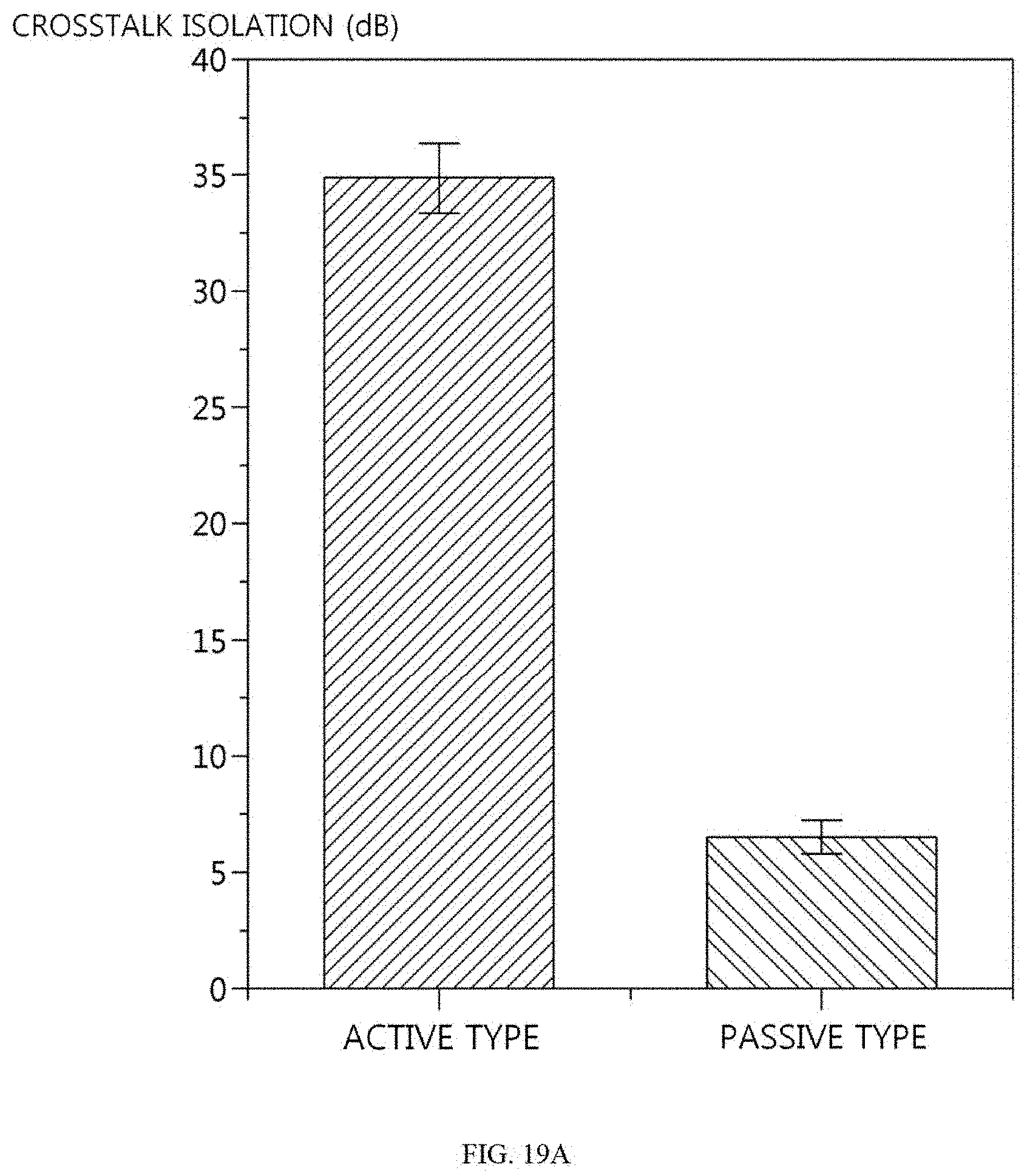
[0171] Referring to FIG. 10A, it is understood that the molybdenum disulfide based backplane in which the Al.sub.2O.sub.3 layer is not deposited has a high contact resistance of 56.7.+-.19.1 ohm-cm at a bottom gate voltage of 150 V but the molybdenum disulfide based backplane in which the channel layer is interposed between the Al.sub.2O.sub.3 layers has a low contact resistance of 5.9.+-.0.7 ohm-cm which is reduced by approximately 10 times.
[0172] The contact region of the channel layer and the source/drain electrode causes a Schottky barrier by a difference in a work function and thus the contact resistance is high. However, a tunnel current is generated by a barrier which becomes thinner due to the electronic doping by depositing the Al.sub.2O.sub.3 layer above the channel layer and the contact resistance becomes lower.
[0173] Referring to FIG. 10B, it is understood that the molybdenum disulfide based backplane in which the Al.sub.2O.sub.3 layer is not deposited has a channel resistance of 15.9.+-.10 MD/cm at a bottom gate voltage of 150 V but the molybdenum disulfide based backplane in which the channel layer is interposed between the Al.sub.2O.sub.3 layers has a channel resistance of 0.1.+-.0.02 M.OMEGA./cm which is reduced by approximately 140 times.
[0174] Referring to FIG. 10C, it is understood that the molybdenum disulfide based backplane having a top gate structure in which channel layer is interposed between the Al.sub.2O.sub.3 layers has a low contact resistance of 5.5.+-.0.6 M.OMEGA./cm and a low channel resistance of 66.5.+-.9.5 k.OMEGA./cm.
[0175] The contact resistance and the channel resistance are reduced and the electron mobility is significantly improved by the upper Al.sub.2O.sub.3 layer. Further, it is understood that the upper Al.sub.2O.sub.3 layer effectively dopes the channel layer in both the channel region and the contact region with the low contact resistance and channel resistance.
[0176] FIG. 11A is a graph illustrating an electrical characteristic of a molybdenum disulfide based backplane formed by a manufacturing method of a transition metal chalcogenide based backplane according to an embodiment of the present disclosure and FIG. 11B illustrates a histogram.
[0177] Referring to FIG. 11A, it is understood that an average mobility for 500 molybdenum disulfide based backplanes with a top gate structure in which the channel layer is interposed between the Al.sub.2O.sub.3 layers is 1.81 cm.sup.2/Vs (a graph inserted at a lower portion).
[0178] Referring to FIG. 11B, it is understood that 500 molybdenum disulfide based backplanes with a top gate structure in which the channel layer is interposed between the Al.sub.2O.sub.3 layers have a high electron mobility of 17 cm.sup.2/Vs to 20 cm.sup.2/Vs, a low hysteresis voltage of 0.75 V or lower, a high ON/OFF ratio of 106 or higher, and a positive threshold voltage V.sub.th of 5.+-.2 V.
[0179] Specifically, the molybdenum disulfide based backplane with a top gate structure in which the channel layer is interposed between the Al.sub.2O.sub.3 layers shows a threshold voltage having a positive value, which allows to maintain an off state of a pixel without supplying an additional gate bias voltage. As a result, unnecessary power consumption at the time of operation of a selective pixel may be reduced.
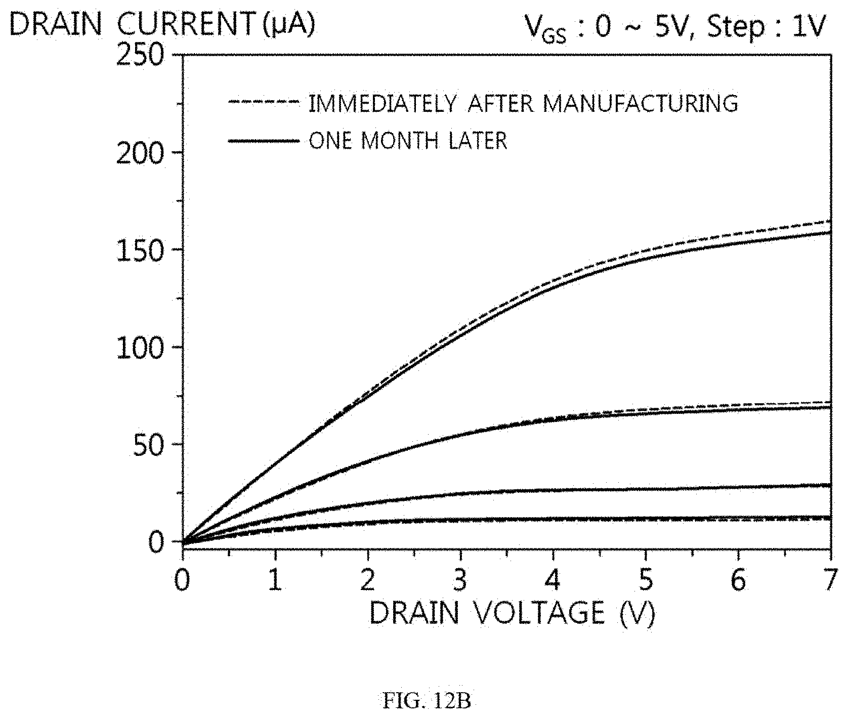
[0180] FIGS. 12A and 12B are graphs illustrating a stability of a molybdenum disulfide based backplane formed by a manufacturing method of a transition metal chalcogenide based backplane according to an embodiment of the present disclosure.
[0181] Referring to FIG. 12A, as a result (a red line) of measuring a switching characteristic one month after manufacturing the molybdenum disulfide based backplane with a top gate structure in which the channel layer is interposed between the Al.sub.2O.sub.3 layers, it is understood that the electron mobility, the ON/OFF ratio, the threshold voltage, and a subthreshold switching value are almost unchanged.
[0182] Referring to FIG. 12B, as a result (a red line) of measuring an output characteristic one month after manufacturing the molybdenum disulfide based backplane with a top gate structure in which the channel layer is interposed between the Al.sub.2O.sub.3 layers, similarly to the switching characteristic, it is understood that the output characteristic is almost unchanged.
[0183] Therefore, it is understood that the molybdenum disulfide based backplane with a top gate structure in which the channel layer is interposed between the Al.sub.23 layers has an excellent reliability and uniformity, so that it is suitable to be applied to an active matrix organic light-emitting diode display.
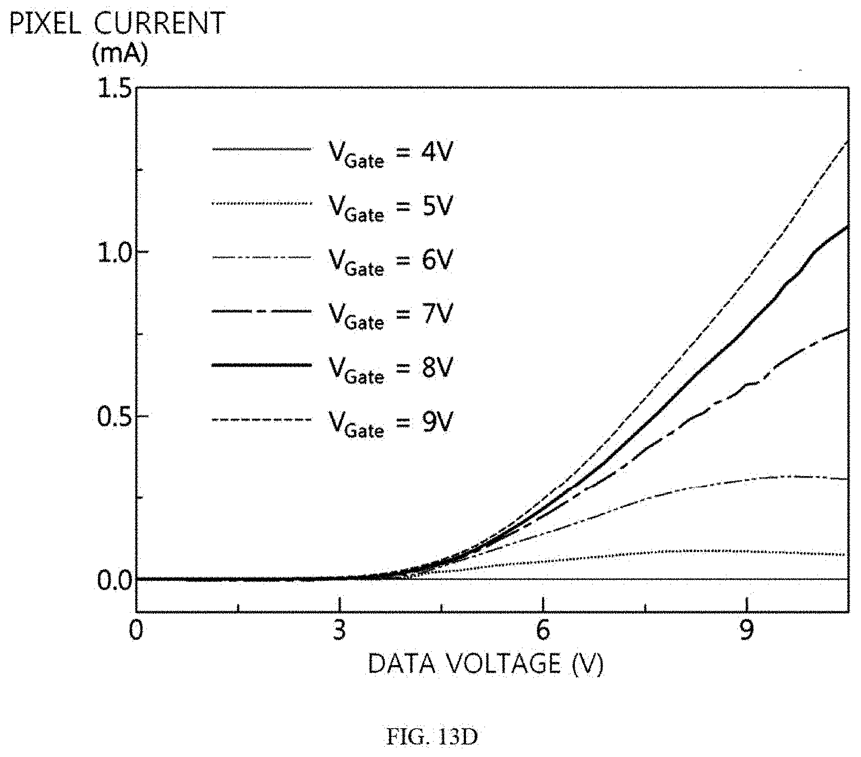
[0184] FIGS. 13A to 13E illustrate a performance of a single pixel of an active matrix organic light-emitting diode which is electrically connected to a molybdenum disulfide based backplane formed by a manufacturing method of a transition metal chalcogenide based backplane according to an embodiment of the present disclosure.
[0185] Referring to FIG. 13A, it is understood that when the luminance is 10 cdm.sup.-2, a turn-on voltage is 4 V and the luminance is linearly increased at a voltage of 8 V or higher to reach .gtoreq.5000 cdm.sup.2 so that the active matrix organic light-emitting diode shows an excellent emission ratio.
[0186] Referring to FIG. 13B, it is understood that when approximately 8 V of V.sub.gate and approximately 9 V of V.sub.Data are applied to the gate electrode and the drain electrode, respectively, the active matrix organic light-emitting diode shows excellent photoluminescence.
[0187] Referring to FIG. 13C, it is understood that when Vo, is increased from 4 V to 9 V at a constant V.sub.Data of approximately 9 V, the emission intensity of the active matrix organic light-emitting diode is distinguishable.
[0188] Further, it is understood that when V.sub.Gate is 9 V, a maximum luminescence reaches 408 cdm.sup.-2, which is sufficiently applicable to the display device, and the molybdenum disulfide based backplane can drive the active matrix organic light-emitting diode.
[0189] Referring to FIG. 13D, it is understood that when V.sub.Gate is increased from 4 V to 9 V an active matrix organic light-emitting diode current I.sub.OLED for different V.sub.Gate values is increased. The active matrix organic light-emitting diode does not operate at low V.sub.Data which is lower than 5 V so that it is understood that I.sub.OLED and V.sub.Gate are independent from each other.
[0190] In contrast, it is understood that the active matrix organic light-emitting diode operates at high V.sub.Data which exceeds 5 V and I.sub.OLED is significantly increased as V.sub.Data is increased and depends on V.sub.Gate.
[0191] Referring to FIG. 13E, the active matrix organic light-emitting diode is quickly turned on and off with respect to a repeated V.sub.Gate pulse of .+-.10V.
[0192] It is understood that a response time is estimated to be 2.5 ms which is limited by a measurement system, but is low enough to drive the active matrix organic light-emitting diode with a short delay time.
[0193] As described above, it is understood that the molybdenum disulfide based backplane formed by the manufacturing method of a transition metal chalcogenide based backplane according to the embodiment of the present disclosure is sufficient to drive the active matrix organic light-emitting diode.
[0194] FIG. 14A illustrates an image when an active matrix organic light-emitting diode display device according to an embodiment of the present disclosure is attached to a wrist of a human and FIG. 14B illustrates a current mapping result during an operation of an active matrix organic light-emitting diode display device.
[0195] Referring to FIG. 14A, it is understood that when the active matrix organic light-emitting diode display device is attached to a human wrist, it is stably attached to a human skin due to a very small thickness (7 .mu.m) of the active matrix organic light-emitting diode display device and representative letters "M", "O", "S", and "2" are sequentially changed on the skin in accordance with the active matrix line addressing.
[0196] The molybdenum disulfide based backplane formed by the manufacturing method of a transition metal chalcogenide based backplane according to the embodiment of the present disclosure has a low bending stiffness due to excellent mechanical characteristic of a molybdenum disulfide layer which is atomically thin.
[0197] Therefore, the low bending stiffness allows conformal contact with the human skin and the excellent mechanical durability of the molybdenum disulfide layer allows the device to be smoothly operated even after being attached to the human skin, and the stable performance for continuous operations may be achieved.
[0198] Referring to FIG. 14B, the ON/OFF mapping corresponding to the representative letter "M" shows that all the pixels (6.times.6 array) function well with the change of ON/OFF current (+2%) without having an external compensation circuit, which confirms the excellent control of the active matrix for the active matrix organic light-emitting diode unit.
[0199] FIG. 15A illustrates an optical image of a process of separating an active matrix organic light-emitting diode display device according to an embodiment of the present disclosure from a carrier substrate and FIG. 15B is a graph illustrating a repeated bending test result with a bending radius of 0.7 mm.
[0200] Referring to FIG. 15A, it is understood that while separating the active matrix organic light-emitting diode display device from a glass substrate which is a carrier substrate, it does not affect the operation of the active matrix organic light-emitting diode display device.
[0201] Further, it is understood that the active matrix organic light-emitting diode display device is flexibly folded due to the low bending stiffness of the active matrix organic light-emitting diode display device.
[0202] Referring to FIG. 15B, in a repeated bending test with a bending radius of 0.7 mm, it is understood that the active matrix organic light-emitting diode display device shows excellent durability and a small current change within 10%.
[0203] It is understood that the small change in current does not affect the operation of the active matrix organic light-emitting diode display device.
[0204] FIG. 16A illustrates a structure of an active matrix tactile sensor including a transition metal chalcogenide based backplane according to an embodiment of the present disclosure and FIG. 16B illustrates an optical image of an active tactile sensor.
[0205] Referring to FIGS. 16A and 16B, it is understood that in an active tactile sensor including a transition metal chalcogenide based backplane (hereinafter, referred to as an "active tactile sensor), each molybdenum disulfide pressure gauge has an active structure which is connected to a molybdenum disulfide based backplane which is a transition metal chalcogenide.
[0206] An active tactile sensor having 8.times.8 array on a large area of 2.8 cm.times.2.8 cm has a thickness of approximately 2.1 .mu.m and a molybdenum disulfide based backplane and molybdenum disulfide pressure gauge may be simultaneously formed using molybdenum disulfide formed by the CVD method.
[0207] Therefore, an active tactile sensor to which the molybdenum disulfide based backplane and the molybdenum disulfide pressure gauge are connected may be formed without performing an addition process.
[0208] A low bending stiffness due to a very small thickness of the active tactile sensor allows the active tactile sensor to be conformally contact with a curved area of the human skin. Further, an initial electrical characteristic may be stably maintained even with a small bending radius.
[0209] FIG. 17A is a graph illustrating a current-voltage characteristic of an active tactile sensor according to an embodiment of the present disclosure, FIG. 17B is a graph illustrating a resistance change in accordance with a time, and FIG. 17C is a graph illustrating a repetitive characteristic in accordance with a pressure.
[0210] Referring to FIG. 17A, it is understood that when a pressure of 0 to 120 kPa is applied to the active tactile sensor according to an embodiment of the present disclosure, as the pressure is increased, the current in an On region is evenly reduced. Further, the current has a constant value in an Off region which is 0 V or lower regardless of the change in pressure.
[0211] Referring to FIG. 17B, it is understood that the resistance of the active tactile sensor according to an embodiment of the present disclosure is evenly reduced in accordance with the pressure so that the output value of the active tactile sensor has a linearity.
[0212] The linearity means that when the pressure is applied, the output characteristic is represented as much as the change. Therefore, in order to accurately measure a magnitude of a constant pressure, it is important that the output value of the sensor has a linearity.
[0213] In the active tactile sensor according to the embodiment of the present disclosure. AR/R.sub.0 shows a resistance change of 0.015 in accordance with a pressure change of approximately 1 kPa in a pressure range of 1 to 120 kPa.
[0214] Therefore, a pressure of at least 1 kPa is sensed, which is a similar sensing area to a skin sensing pressure of 1 to 100 kPa so that the active tactile sensor according to the embodiment of the present disclosure may be utilized as an electronic skin.
[0215] Further, it is understood that when a pressure is applied for approximately 13 seconds at every pressure of 1 to 120 kPa, constant resistance change is maintained in the active tactile sensor according to the embodiment of the present disclosure and a response time is 180 ms when a pressure of 1 kPa is applied.
[0216] Referring to FIG. 17C, it is understood that the active tactile sensor according to the embodiment of the present disclosure maintains a unique resistance change characteristic for 10000 cycles in accordance with a pressure of 1 to 120 kPa and a very low drift characteristic is shown at a pressure of 120 kPa.
[0217] FIGS. 18A to 18D are graphs illustrating a flexible characteristic of an active tactile sensor according to an embodiment of the present disclosure.
[0218] Referring to FIG. 18A, it is understood that a large area active tactile sensor according to the embodiment of the present disclosure has a total thickness of approximately 2.1 .mu.m and has an excellent flexible characteristic so that the tactile sensor completely wraps a glass pipet having a diameter of 1 mm.
[0219] Referring to an inserted image, when the active tactile sensor is enlarged, no crack is found so that it is understood that it has an excellent mechanical characteristic.
[0220] The excellent flexible characteristic allows the pressure to be accurately detected without being affected by a resistance change due to mechanical deformation such as bending, twisting, wrinkle generated on a soft substrate like a human skin.
[0221] Referring to FIGS. 18B to 18D, when the active tactile sensor is bent until the bending radius becomes 3 mm, the molybdenum disulfide based backplane shows a stable switching characteristic and the molybdenum disulfide pressure gauge shows a stable linearity.
[0222] The mobility of the molybdenum disulfide based backplane and the resistance characteristic of the molybdenum disulfide pressure gauge maintain a stable characteristic with a value of 0.8 to 0.9 of .DELTA.R/R.sub.0 at each bending radius and an initial characteristic is well recovered without lowering the characteristic.
[0223] The bending test shows that the active tactile sensor maintains the stable characteristic even in the mechanical deformation due to the bending of the human skin or palm.
[0224] FIG. 19A is a graph illustrating a low crosstalk characteristic of an active tactile sensor according to an embodiment of the present disclosure, FIG. 19B is a graph illustrating a resistance change of an active tactile sensor, and FIG. 19C is an image illustrating pressure mapping when letters are input on an active tactile sensor.
[0225] Referring to FIG. 19A, the active tactile sensor has a crosstalk isolation value of 24.80 dB, but the passive tactile sensor has 6.6 dB which is approximately four times lower.
[0226] In the passive tactile sensor, a resistance change of a cell to which the pressure is applied affects a proximate cell so that a crosstalk characteristic is high. In contrast, in the active tactile sensor, the backplane which is connected to the cell reduces the influence for the proximate cell, so that the crosstalk characteristic is low.
[0227] FIG. 19B illustrates that as a result of mapping a pressure after putting a small miniature chair on an active tactile sensor, the pressure is accurately sensed without causing a crosstalk and .DELTA.R/R.sub.0 is 0.95.
[0228] FIG. 19C illustrates that when a letter "M" is quickly input on the active tactile sensor using a touch pen, a pressure which is applied to each cell on a pressure mapping screen at a real time is accurately and quickly sensed.
[0229] It is understood that the active tactile sensor can be utilized as a real-time information input device with a low crosstalk characteristic and a quick response time of the active tactile sensor.
[0230] FIG. 20 illustrates a resistance change when an active tactile sensor is bonded onto a palm and then a light object is held in an active tactile sensor according to an embodiment of the present disclosure.
[0231] Referring to FIG. 20, it is understood that when an apple is held with an active tactile sensor attached to a palm of the hand, a resistance change is approximately 0.1 to 0.8 in accordance with a change of a state holding the apple and a shape of a contact region and a change in an applied pressure are sensed.
[0232] As described above, although the present invention has been described by limited embodiments and drawings, the present invention is not limited to the embodiments, and it will be apparent to those skilled in the art to which the present invention pertains that various modifications and variations may be made from the description.
[0233] Accordingly, the scope of the present invention is not construed as being limited to the described embodiments but is defined by the appended claims as well as equivalents thereto.
* * * * *
D00000
D00001
D00002
D00003
D00004
D00005
D00006
D00007
D00008
D00009
D00010
D00011
D00012

D00013

D00014

D00015

D00016

D00017

D00018
D00019

D00020

D00021
D00022

D00023

D00024

D00025

D00026

D00027

D00028

D00029

D00030

D00031

D00032

D00033

D00034

D00035
D00036

D00037

D00038

D00039
D00040

D00041

D00042

D00043

D00044

D00045

D00046

D00047

D00048

D00049

D00050

D00051

D00052

D00053

D00054
D00055

D00056

D00057

XML
uspto.report is an independent third-party trademark research tool that is not affiliated, endorsed, or sponsored by the United States Patent and Trademark Office (USPTO) or any other governmental organization. The information provided by uspto.report is based on publicly available data at the time of writing and is intended for informational purposes only.
While we strive to provide accurate and up-to-date information, we do not guarantee the accuracy, completeness, reliability, or suitability of the information displayed on this site. The use of this site is at your own risk. Any reliance you place on such information is therefore strictly at your own risk.
All official trademark data, including owner information, should be verified by visiting the official USPTO website at www.uspto.gov. This site is not intended to replace professional legal advice and should not be used as a substitute for consulting with a legal professional who is knowledgeable about trademark law.