Wide Bandwidth Time Division Duplex Transceiver
Reisner; Russ ; et al.
U.S. patent application number 17/108977 was filed with the patent office on 2021-04-22 for wide bandwidth time division duplex transceiver. The applicant listed for this patent is Resonant Inc.. Invention is credited to Neal Fenzi, Bryant Garcia, Robert B. Hammond, Russ Reisner, Patrick Turner.
| Application Number | 20210119603 17/108977 |
| Document ID | / |
| Family ID | 1000005303310 |
| Filed Date | 2021-04-22 |


| United States Patent Application | 20210119603 |
| Kind Code | A1 |
| Reisner; Russ ; et al. | April 22, 2021 |
WIDE BANDWIDTH TIME DIVISION DUPLEX TRANSCEIVER
Abstract
A wide bandwidth time division duplex (TDD) transceiver includes a transmitter, a receiver, and a bandpass filter implemented with a plurality of acoustic resonators including at least one shunt resonator and at least one series resonator. A transmit/receive switch is configured to selectively connect a first terminal of the bandpass filter to either an output of the transmitter or an input of the receiver. Each of the plurality of acoustic resonators is a high power transversely-excite film bulk acoustic resonator.
| Inventors: | Reisner; Russ; (Oxnard, CA) ; Fenzi; Neal; (Santa Barbara, CA) ; Hammond; Robert B.; (Santa Barbara, CA) ; Turner; Patrick; (San Bruno, CA) ; Garcia; Bryant; (Burlingame, CA) | ||||||||||
| Applicant: |
|
||||||||||
|---|---|---|---|---|---|---|---|---|---|---|---|
| Family ID: | 1000005303310 | ||||||||||
| Appl. No.: | 17/108977 | ||||||||||
| Filed: | December 1, 2020 |
Related U.S. Patent Documents
| Application Number | Filing Date | Patent Number | ||
|---|---|---|---|---|
| 16829617 | Mar 25, 2020 | 10868512 | ||
| 17108977 | ||||
| 16578811 | Sep 23, 2019 | 10637438 | ||
| 16829617 | ||||
| 16230443 | Dec 21, 2018 | 10491192 | ||
| 16578811 | ||||
| 62685825 | Jun 15, 2018 | |||
| 62701363 | Jul 20, 2018 | |||
| 62741702 | Oct 5, 2018 | |||
| 62748883 | Oct 22, 2018 | |||
| 62753815 | Oct 31, 2018 | |||
| Current U.S. Class: | 1/1 |
| Current CPC Class: | H03H 9/02 20130101; H03H 9/02015 20130101; H03H 9/171 20130101; H03H 9/13 20130101; H03H 9/54 20130101 |
| International Class: | H03H 9/17 20060101 H03H009/17; H03H 9/54 20060101 H03H009/54; H03H 9/02 20060101 H03H009/02 |
Claims
1. A wide bandwidth time division duplex (TDD) transceiver comprising: a transmitter; a receiver; a bandpass filter comprising a plurality of acoustic resonators including at least one shunt resonator and at least one series resonator; and a transmit/receive switch configured to selectively connect a first port of the bandpass filter to either an output of the transmitter or an input of the receiver, wherein each of the plurality of acoustic resonators is a high power transversely-excite film bulk acoustic resonator.
2. The TDD transceiver of claim 1, each of the plurality of acoustic resonators further comprising: a piezoelectric diaphragm; and an interdigital transducer (IDT) with interleaved fingers disposed on a surface of the piezoelectric diaphragm, a thickness of the interleaved fingers of the IDT greater than or equal to 0.85 times a thickness of the piezoelectric diaphragm and less than or equal to 2.5 times the thickness of the piezoelectric diaphragm.
3. The TDD transceiver of claim 2, wherein for each of the plurality of acoustic resonators, the piezoelectric diaphragm and the IDT are configured such that a respective radio frequency signal applied to the IDT excites a respective primary shear acoustic mode in the piezoelectric diaphragm.
4. The TDD transceiver of claim 2, wherein the interleaved fingers of the IDTs of the plurality of acoustic resonators are substantially aluminum.
5. The TDD transceiver of claim 4, wherein the at least one shunt resonator further comprises a dielectric frequency setting layer having a thickness greater than zero and less than or equal to 0.25 times the thickness of the piezoelectric diaphragm, and the thickness of the interleaved fingers of the IDTs of the at least one shunt resonator is greater than or equal to 0.875 times the thickness of the piezoelectric diaphragm and less than or equal to 2.25 times the thickness of the piezoelectric diaphragm.
6. The TDD transceiver of claim 2, wherein the interleaved fingers of the IDTs of the plurality of acoustic resonators are substantially copper, and the thickness of the interleaved fingers of the IDTs of the plurality of acoustic resonators is within a first range of greater than or equal to 0.85 times the thickness of the piezoelectric plate and less than or equal to 1.42 times the thickness of the piezoelectric plate, or within a second range of greater than or equal to 1.95 times the thickness of the piezoelectric plate and less than or equal to 2.325 times the thickness of the piezoelectric plate.
7. The TDD transceiver of claim 6, wherein: the at least one shunt resonator further comprises a dielectric frequency setting layer having a thickness greater than zero and less than or equal to 0.25 times the thickness of the piezoelectric diaphragm, and the thickness of the interleaved fingers of the IDTs of the at least one shunt resonator is within the first range of greater than or equal to 0.85 times the thickness of the piezoelectric diaphragm and less than or equal to 1.42 times the thickness of the piezoelectric diaphragm.
8. The TDD transceiver of claim 1, wherein: a second port of the bandpass filter is configured to connect to an antenna.
9. A wide bandwidth time division duplex (TDD) transceiver comprising: a transmitter; a receiver; a bandpass filter; and a transmit/receive switch configured to selectively connect a first port of the bandpass filter to either an output of the transmitter or an input of the receiver, wherein the bandpass filter further comprises: a substrate; a single-crystal piezoelectric plate having front and back surfaces, the back surface attached to a surface of the substrate, portions of the single-crystal piezoelectric plate forming one or more diaphragms spanning respective cavities in the substrate; a conductor pattern formed on the front surface, the conductor pattern including a plurality of interdigital transducers (IDTs) of a respective plurality acoustic resonators, interleaved fingers of each of the plurality of IDTs disposed on one of the one or more diaphragms, the plurality of acoustic resonators including one or more shunt resonators and one or more series resonators.
10. The TDD transceiver of claim 9, wherein the interleaved fingers of the plurality of IDTs are substantially aluminum, and a thickness of the interleaved fingers of the plurality of IDTs is greater than or equal to 0.85 times a thickness of the piezoelectric plate and less than or equal to 2.5 times the thickness of the piezoelectric plate.
11. The TDD transceiver of claim 10, wherein the at least one shunt resonator further comprises a dielectric frequency setting layer having a thickness greater than zero and less than or equal to 0.25 times the thickness of the piezoelectric plate, and the thickness of the interleaved fingers of the plurality of IDTs is greater than or equal to 0.875 times the thickness of the piezoelectric plate and less than or equal to 2.25 times the thickness of the piezoelectric plate.
12. The TDD transceiver of claim 9, wherein the interleaved fingers of the plurality of IDTs are substantially copper, and the thickness of the interleaved fingers of the plurality of IDTs is within a first range of greater than or equal to 0.85 times the thickness of the piezoelectric plate and less than or equal to 1.42 times the thickness of the piezoelectric plate, or with a second range of greater than or equal to 1.95 times the thickness of the piezoelectric plate and less than or equal to 2.325 times the thickness of the piezoelectric plate.
13. The TDD transceiver of claim 12, wherein: the at least one shunt resonator further comprises a dielectric frequency setting layer having a thickness greater than zero and less than or equal to 0.25 times the thickness of the piezoelectric plate, and the thickness of the interleaved fingers of the plurality of IDTs is with the first range of greater than or equal to 0.85 times the thickness of the piezoelectric plate and less than or equal to 1.42 times the thickness of the piezoelectric plate.
14. The TDD transceiver of claim 9, wherein, for each of the plurality of acoustic resonators, the piezoelectric plate and the IDT are configured such that a respective radio frequency signal applied to the IDT excites a respective primary shear acoustic mode in the diaphragm.
15. The TDD transceiver of claim 9, wherein: a second port of the bandpass filter is configured to connect to an antenna.
16. The TDD transceiver of claim 9, wherein: each of the plurality of acoustic resonators is a high power transversely-excited film bulk acoustic resonator.
17. A diplexer for a dual channel time division duplex (TDD) transceiver comprising: a low band bandpass filter comprising a first port, a second port, and a first plurality of acoustic resonators; and a high band bandpass filter comprising a first port, a second port, and a second plurality of acoustic resonators, wherein wherein each acoustic resonator of the first and second pluralities of acoustic resonators is a high power transversely-excited film bulk acoustic resonators, and the second port of the low band bandpass filter and the second port of the high band bandpass filter are connected to a common port configured for connection to an antenna.
18. The diplexer of claim 16, wherein each acoustic resonator of the first and second pluralities of acoustic resonators comprises: a piezoelectric diaphragm; and an interdigital transducer (IDT) with interleaved fingers disposed on a surface of the diaphragm, wherein a thickness of the interleaved fingers of the IDT is greater than or equal to 0.85 times a thickness of the piezoelectric diaphragm and less than or equal to 2.5 times the thickness of the piezoelectric diaphragm.
19. The diplexer of claim 17, wherein the piezoelectric diaphragm and IDT of each acoustic resonator of the first and second pluralities of acoustic resonators are configured such that a respective radio frequency signal applied to the IDT excites a respective primary shear acoustic mode in the piezoelectric diaphragm.
Description
RELATED APPLICATION INFORMATION
[0001] This patent is a continuation-in-part of application Ser. No. 16/829,617, filed Mar. 25, 2020, entitled HIGH POWER TRANSVERSLEY-EXCITED FILM BULK ACOUSTIC RESONATOR ON Z-CUT LITHIUM NIOBATE, which is a continuation of application Ser. No. 16/578,811, filed Sep. 23, 2019, entitled TRANSVERSELY-EXCITED FILM BULK ACOUSTIC RESONATORS FOR HIGH POWER APPLICATIONS, now U.S. Pat. No. 10,637,438, which is a continuation-in-part of application Ser. No. 16/230,443, filed Dec. 21, 2018, entitled TRANSVERSELY-EXCITED FILM BULK ACOUSTIC RESONATOR, now U.S. Pat. No. 10,491,192, which claims priority from the following provisional patent applications: application 62/685,825, filed Jun. 15, 2018, entitled SHEAR-MODE FBAR (XBAR); application 62/701,363, filed Jul. 20, 2018, entitled SHEAR-MODE FBAR (XBAR); application 62/741,702, filed Oct. 5, 2018, entitled 5 GHZ LATERALLY-EXCITED BULK WAVE RESONATOR (XBAR); application 62/748,883, filed Oct. 22, 2018, entitled SHEAR-MODE FILM BULK ACOUSTIC RESONATOR; and application 62/753,815, filed Oct. 31, 2018, entitled LITHIUM TANTALATE SHEAR-MODE FILM BULK ACOUSTIC RESONATOR. All of these applications are incorporated herein by reference.
NOTICE OF COPYRIGHTS AND TRADE DRESS
[0002] A portion of the disclosure of this patent document contains material which is subject to copyright protection. This patent document may show and/or describe matter which is or may become trade dress of the owner. The copyright and trade dress owner has no objection to the facsimile reproduction by anyone of the patent disclosure as it appears in the Patent and Trademark Office patent files or records, but otherwise reserves all copyright and trade dress rights whatsoever.
BACKGROUND
Field
[0003] This disclosure relates to radio frequency filters using acoustic wave resonators, and specifically to filters for use in communications equipment.
Description of the Related Art
[0004] A radio frequency (RF) filter is a two-port device configured to pass some frequencies and to stop other frequencies, where "pass" means transmit with relatively low signal loss and "stop" means block or substantially attenuate. The range of frequencies passed by a filter is referred to as the "pass-band" of the filter. The range of frequencies stopped by such a filter is referred to as the "stop-band" of the filter. A typical RF filter has at least one pass-band and at least one stop-band. Specific requirements on a passband or stop-band depend on the application. For example, a "pass-band" may be defined as a frequency range where the insertion loss of a filter is better than a defined value such as 1 dB, 2 dB, or 3 dB. A "stop-band" may be defined as a frequency range where the rejection of a filter is greater than a defined value such as 20 dB, 30 dB, 40 dB, or greater depending on application.
[0005] RF filters are used in communications systems where information is transmitted over wireless links. For example, RF filters may be found in the RF front-ends of cellular base stations, mobile telephone and computing devices, satellite transceivers and ground stations, IoT (Internet of Things) devices, laptop computers and tablets, fixed point radio links, and other communications systems. RF filters are also used in radar and electronic and information warfare systems.
[0006] RF filters typically require many design trade-offs to achieve, for each specific application, the best compromise between performance parameters such as insertion loss, rejection, isolation, power handling, linearity, size and cost. Specific design and manufacturing methods and enhancements can benefit simultaneously one or several of these requirements.
[0007] Performance enhancements to the RF filters in a wireless system can have broad impact to system performance. Improvements in RF filters can be leveraged to provide system performance improvements such as larger cell size, longer battery life, higher data rates, greater network capacity, lower cost, enhanced security, higher reliability, etc. These improvements can be realized at many levels of the wireless system both separately and in combination, for example at the RF module, RF transceiver, mobile or fixed sub-system, or network levels.
[0008] High performance RF filters for present communication systems commonly incorporate acoustic wave resonators including surface acoustic wave (SAW) resonators, bulk acoustic wave (BAW) resonators, film bulk acoustic wave resonators (FBAR), and other types of acoustic resonators. However, these existing technologies are not well-suited for use at the higher frequencies and bandwidths proposed for future communications networks.
[0009] The desire for wider communication channel bandwidths will inevitably lead to the use of higher frequency communications bands. Radio access technology for mobile telephone networks has been standardized by the 3GPP (3.sup.rd Generation Partnership Project). Radio access technology for 5.sup.th generation (5G) mobile networks is defined in the 5G NR (new radio) standard. The 5G NR standard defines several new communications bands. Two of these new communications bands are n77, which uses the frequency range from 3300 MHz to 4200 MHz, and n79, which uses the frequency range from 4400 MHz to 5000 MHz. Both band n77 and band n79 use time-division duplexing (TDD), such that a communications device operating in band n77 and/or band n79 use the same frequencies for both uplink and downlink transmissions. Bandpass filters for bands n77 and n79 must be capable of handling the transmit power of the communications device. WiFi bands at 5 GHz and 6 GHz also require high frequency and wide bandwidth. The 5G NR standard also defines millimeter wave communication bands with frequencies between 24.25 GHz and 40 GHz.
[0010] The Transversely-Excited Film Bulk Acoustic Resonator (XBAR) is an acoustic resonator structure for use in microwave filters. The XBAR is described in U.S. Pat. No. 10,491,291, titled TRANSVERSELY EXCITED FILM BULK ACOUSTIC RESONATOR. An XBAR resonator comprises an interdigital transducer (IDT) formed on a thin floating layer, or diaphragm, of a single-crystal piezoelectric material. The IDT includes a first set of parallel fingers, extending from a first busbar and a second set of parallel fingers extending from a second busbar. The first and second sets of parallel fingers are interleaved. A microwave signal applied to the IDT excites a shear primary acoustic wave in the piezoelectric diaphragm. XBAR resonators provide very high electromechanical coupling and high frequency capability. XBAR resonators may be used in a variety of RF filters including band-reject filters, band-pass filters, duplexers, and multiplexers. XBARs are well suited for use in filters for communications bands with frequencies above 3 GHz.
DESCRIPTION OF THE DRAWINGS
[0011] FIG. 1 is a block diagram of a broad band time division duplex transceiver.
[0012] FIG. 2 includes a schematic plan view and two schematic cross-sectional views of a transversely-excited film bulk acoustic resonator (XBAR).
[0013] FIG. 3 is an expanded schematic cross-sectional view of a portion of the XBAR of FIG. 3.
[0014] FIG. 4 is a schematic circuit diagram of a band-pass filter using acoustic resonators in a ladder filter circuit.
[0015] FIG. 5A is a schematic cross-sectional view of a filter with a dielectric frequency setting layer to set a frequency separation between shunt resonators and series resonators.
[0016] FIG. 5B is a schematic cross-sectional view of a filter with different piezoelectric diaphragm thicknesses to set a frequency separation between shunt resonators and series resonators.
[0017] FIG. 6 is a block diagram of a dual-band time division duplex transceiver.
[0018] Throughout this description, elements appearing in figures are assigned three-digit or four-digit reference designators, where the two least significant digits are specific to the element and the one or two most significant digit is the figure number where the element is first introduced. An element that is not described in conjunction with a figure may be presumed to have the same characteristics and function as a previously-described element having the same reference designator.
DETAILED DESCRIPTION
[0019] Description of Apparatus
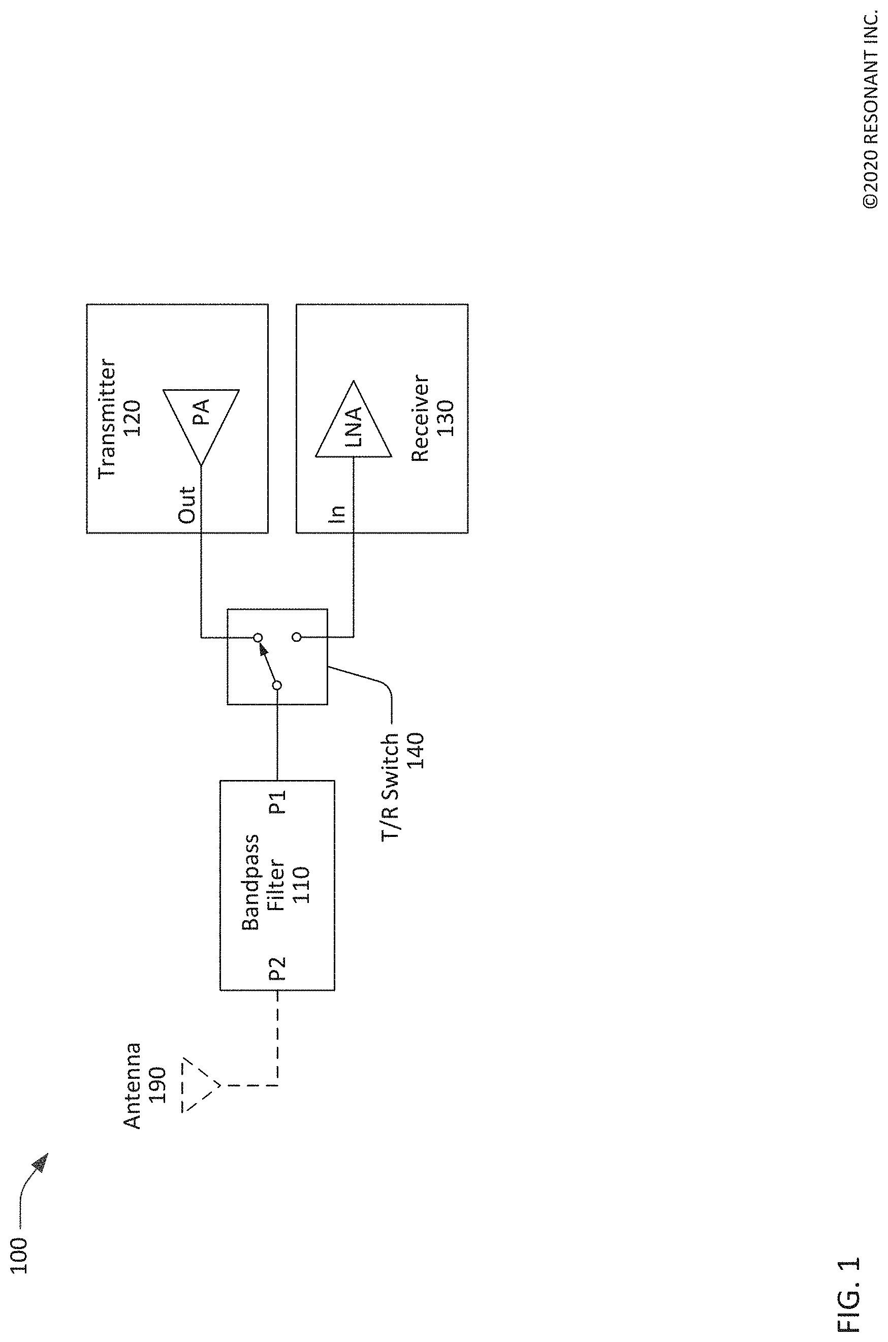
[0020] FIG. 1 is a schematic block diagram of a wide bandwidth time division duplex (TDD) transceiver 100. The transceiver 100 includes a bandpass filter 110 having a first port P1 coupled to a transmit/receive (T/R) switch 140 a second port P2 configured for connection to an antenna 190. The antenna and the connection from the bandpass filter 110 to the antenna are not part of the transceiver 100 and are shown in dashed lines. The T/R switch 140 connects the second port of the bandpass filter 110 to either the output of a transmitter 120 or the input of a receiver 130. The T/R switch 140, the transmitter 120, and the receiver 130 are supervised by a processor (not shown) performing a media access control function.
[0021] The transceiver 100 is configured for operation in a designated communications band. The bandpass filter 110 has a pass band that encompasses the designated communications band and one or more stop bands to block designated frequencies outside of the designated communications band. Preferably, the bandpass filter 110 has low loss in its pass band and high rejection in is stop band(s). Further, the bandpass filter 110 must be compatible, which is to say stable and reliable, while passing the RF power generated by the transmitter 120.
[0022] The bandpass filter 110 may be implemented using transversely-excited film bulk acoustic resonators (XBARs). XBAR filters are particularly appropriate for TDD communications bands at frequencies above 3 GHz, including 5G NR bands n77 and n79, and 5 GHz and 6 GHz WiFi bands.
[0023] FIG. 2 shows a simplified schematic top view and orthogonal cross-sectional views of an XBAR 200. XBAR resonators such as the resonator 200 may be used in a variety of RF filters including band-reject filters, band-pass filters such as the bandpass filter 110, duplexers, and multiplexers.
[0024] The XBAR 200 is made up of a thin film conductor pattern formed on a surface of a piezoelectric plate 210 having parallel front and back surfaces 212, 214, respectively. The piezoelectric plate is a thin single-crystal layer of a piezoelectric material such as lithium niobate, lithium tantalate, lanthanum gallium silicate, gallium nitride, or aluminum nitride. The piezoelectric plate is cut such that the orientation of the X, Y, and Z crystalline axes with respect to the front and back surfaces is known and consistent. The piezoelectric plate may be Z-cut, which is to say the Z axis is normal to the front and back surfaces 212, 214. The piezoelectric plate may be rotated Z-cut or rotated YX-cut. XBARs may be fabricated on piezoelectric plates with other crystallographic orientations.
[0025] The back surface 214 of the piezoelectric plate 210 is attached to a surface of the substrate 220 except for a portion of the piezoelectric plate 210 that forms a diaphragm 215 spanning a cavity 240 formed in the substrate. The portion of the piezoelectric plate that spans the cavity is referred to herein as the "diaphragm" 215 due to its physical resemblance to the diaphragm of a microphone. As shown in FIG. 2, the diaphragm 215 is contiguous with the rest of the piezoelectric plate 210 around all of a perimeter 245 of the cavity 240. In this context, "contiguous" means "continuously connected without any intervening item". In other configurations, the diaphragm 215 may be contiguous with the piezoelectric plate are at least 50% of the perimeter 245 of the cavity 240.
[0026] The substrate 220 provides mechanical support to the piezoelectric plate 210. The substrate 220 may be, for example, silicon, sapphire, quartz, or some other material or combination of materials. The back surface 214 of the piezoelectric plate 210 may be bonded to the substrate 220 using a wafer bonding process. Alternatively, the piezoelectric plate 210 may be grown on the substrate 220 or attached to the substrate in some other manner. The piezoelectric plate 210 may be attached directly to the substrate or may be attached to the substrate 220 via one or more intermediate material layers (not shown in FIG. 2).
[0027] "Cavity" has its conventional meaning of "an empty space within a solid body." The cavity 240 may be a hole completely through the substrate 220 (as shown in Section A-A and Section B-B) or a recess in the substrate 220 under the diaphragm 215. The cavity 240 may be formed, for example, by selective etching of the substrate 220 before or after the piezoelectric plate 210 and the substrate 220 are attached.
[0028] The conductor pattern of the XBAR 200 includes an interdigital transducer (IDT) 230. The IDT 230 includes a first plurality of parallel fingers, such as finger 236, extending from a first busbar 232 and a second plurality of fingers extending from a second busbar 234. The first and second pluralities of parallel fingers are interleaved. The interleaved fingers overlap for a distance AP, commonly referred to as the "aperture" of the IDT. The center-to-center distance L between the outermost fingers of the IDT 230 is the "length" of the IDT.
[0029] The first and second busbars 232, 234 serve as the terminals of the XBAR 200. A radio frequency or microwave signal applied between the two busbars 232, 234 of the IDT 230 excites a primary acoustic mode within the piezoelectric plate 210. The primary acoustic mode is a bulk shear mode where acoustic energy propagates along a direction substantially orthogonal to the surface of the piezoelectric plate 210, which is also normal, or transverse, to the direction of the electric field created by the IDT fingers. Thus, the XBAR is considered a transversely-excited film bulk wave resonator.
[0030] The IDT 230 is positioned on the piezoelectric plate 210 such that at least the fingers of the IDT 230 are disposed on the diaphragm 215 that spans, or is suspended over, the cavity 240. As shown in FIG. 2, the cavity 240 has a rectangular shape with an extent greater than the aperture AP and length L of the IDT 230. A cavity of an XBAR may have a different shape, such as a regular or irregular polygon. The cavity of an XBAR may more or fewer than four sides, which may be straight or curved.
[0031] For ease of presentation in FIG. 2, the geometric pitch and width of the IDT fingers is greatly exaggerated with respect to the length (dimension L) and aperture (dimension AP) of the XBAR. A typical XBAR has more than ten parallel fingers in the IDT 210. An XBAR may have hundreds, possibly thousands, of parallel fingers in the IDT 210. Similarly, the thicknesses of the IDT fingers and the piezoelectric plate in the cross-sectional views are greatly exaggerated.
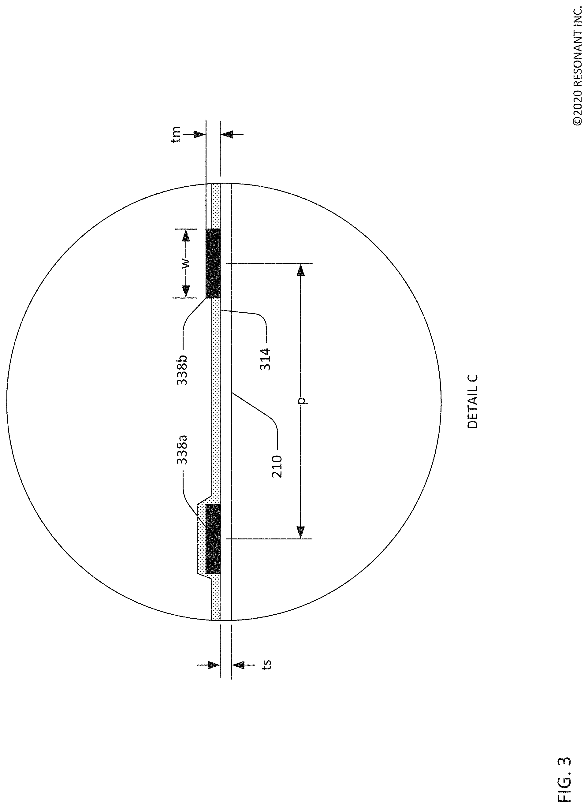
[0032] FIG. 3 shows a detailed schematic cross-sectional view of the XBAR 200. The piezoelectric plate 210 is a single-crystal layer of piezoelectrical material having a thickness ts. ts may be, for example, 100 nm to 1500 nm. When used in filters for communications bands from 3.4 GHZ to 6 GHz, the thickness ts may be, for example, 200 nm to 1000 nm.
[0033] A front-side dielectric layer 314 may optionally be formed on the front side of the piezoelectric plate 210. The "front side" of the XBAR is, by definition, the surface facing away from the substrate. The front-side dielectric layer 314 may be formed only between the IDT fingers (e.g. IDT finger 338b) or may be deposited as a blanket layer such that the dielectric layer is formed both between and over the IDT fingers (e.g. IDT finger 338a). The front-side dielectric layer 314 may be a non-piezoelectric dielectric material, such as silicon dioxide, alumina, or silicon nitride. tfd may be, for example, 0 to 500 nm. tfd is typically less than about one-third of the thickness is of the piezoelectric plate. The front-side dielectric layer 314 may be formed of multiple layers of two or more materials. In some applications, a back-side dielectric layer (not shown) may be formed on the back side of the piezoelectric plate 210.
[0034] The IDT fingers 338a, 338b may be aluminum, an aluminum alloy, copper, a copper alloy, beryllium, gold, tungsten, molybdenum or some other conductive material. The IDT fingers are considered to be "substantially aluminum" if they are formed from aluminum or an alloy comprising at least 50% aluminum. The IDT fingers are considered to be "substantially copper" if they are formed from copper or an alloy comprising at least 50% copper. Thin (relative to the total thickness of the conductors) layers of other metals, such as chromium or titanium, may be formed under and/or over and/or as layers within the fingers to improve adhesion between the fingers and the piezoelectric plate 210 and/or to passivate or encapsulate the fingers and/or to improve power handling. The busbars (232, 234 in FIG. 2) of the IDT may be made of the same or different materials as the fingers.
[0035] Dimension p is the center-to-center spacing or "pitch" of the IDT fingers, which may be referred to as the pitch of the IDT and/or the pitch of the XBAR. Dimension w is the width or "mark" of the IDT fingers. The geometry of the IDT of an XBAR differs substantially from the IDTs used in surface acoustic wave (SAW) resonators. In a SAW resonator, the pitch of the IDT is one-half of the acoustic wavelength at the resonance frequency. Additionally, the mark-to-pitch ratio of a SAW resonator IDT is typically close to 0.5 (i.e. the mark or finger width is about one-fourth of the acoustic wavelength at resonance). In an XBAR, the pitch p of the IDT is typically 2 to 20 times the width w of the fingers. In addition, the pitch p of the IDT is typically 2 to 20 times the thickness is of the piezoelectric plate 210. The width of the IDT fingers in an XBAR is not constrained to be near one-fourth of the acoustic wavelength at resonance. For example, the width of XBAR IDT fingers may be 500 nm or greater, such that the IDT can be readily fabricated using optical lithography. The thickness tm of the IDT fingers may be from 100 nm to about equal to the width w. The thickness of the busbars (232, 234 in FIG. 2) of the IDT may be the same as, or greater than, the thickness tm of the IDT fingers.
[0036] FIG. 4 is a schematic circuit diagram for a high frequency band-pass filter 400 using XBARs. The filter 400 has a conventional ladder filter architecture including four series resonators 410A, 410B, 410C, 410D and three shunt resonators 420A, 420B, 420C. The four series resonators 410A, 410B, 410C, and 410D are connected in series between a first port and a second port. In FIG. 4, the first and second ports are labeled "In" and "Out", respectively. However, the filter 400 is symmetrical and either port and serve as the input or output of the filter. The three shunt resonators 420A, 420B, 420C are connected from nodes between the series resonators to ground. All the shunt resonators and series resonators are XBARs. Although not shown in FIG. 4, none, some, or all of the resonators may be divided into multiple sub-resonators electrically connected in parallel. Each sub-resonator may have a respective diaphragm.
[0037] In a ladder filter, such as the filter 400, the resonance frequencies of shunt resonators are typically lower than the resonance frequencies of series resonators. The resonance frequency of an SM XBAR resonator is determined, in part, by IDT pitch. IDT pitch also impacts other filter parameters including impedance and power handling capability. For broad-band filter applications, it may not be practical to provide the required difference between the resonance frequencies of shunt and series resonators using only differences in IDT pitch.
[0038] As described in U.S. Pat. No. 10,601,392, a first dielectric layer (represented by the dashed rectangle 425) having a first thickness t1 may be deposited over the IDTs of some or all of the shunt resonators 420A, 420B, 420C. A second dielectric layer (represented by the dashed rectangle 415) having a second thickness t2, less than t1, may be deposited over the IDTs of the series resonators 410A, 410B, 410C, 410D. The second dielectric layer may be deposited over both the shunt and series resonators. The difference between the thickness t1 and the thickness t2 defines a frequency offset between the series and shunt resonators. Individual series or shunt resonators may be tuned to different frequencies by varying the pitch of the respective IDTs. In some filters, more than two dielectric layers of different thicknesses may be used as described in co-pending application Ser. No. 16/924,108.
[0039] Alternatively or additionally, the shunt resonators 410A, 410B, 410C, 410D may be formed on a piezoelectric plate having a thickness t3 and the series resonators 420A, 420B, 420C may be fabricated on a piezoelectric plate having a thickness t4 less than t3. The difference between the thicknesses t3 and t4 defines a frequency offset between the series and shunt resonators. Individual series or shunt resonators may be tuned to different frequencies by varying the pitch of the respective IDTs. In some filters, three or more different piezoelectric plate thicknesses may be used to provide additional frequency tuning capability.
[0040] The filter 400 is exemplary. A bandpass filter may have more or fewer than seven resonators, more or fewer than four series resonators, and nor or fewer than three shunt resonators. Most filters will have at least three resonators including at least on shunt resonator and one series resonator. Filters may include additional reactive components, such as inductors and/or capacitors that are not shown in FIG. 4.
[0041] FIG. 5A is a schematic cross-sectional view though a shunt resonator and a series resonator of a filter 500A that uses dielectric thickness to separate the frequencies of shunt and series resonators. A piezoelectric plate 510A is attached to a substrate 520. Portions of the piezoelectric plate form diaphragms spanning cavities 540 in the substrate 520. Interleaved IDT fingers, such as finger 530, are formed on the diaphragms. A first dielectric layer 550, having a thickness t1, is formed over the IDT of the shunt resonator. A second dielectric layer 555, having a thickness t2, is deposited over both the shunt and series resonators. Alternatively, a single dielectric layer having thickness t1+t2 may be deposited over both the shunt and series resonators. The dielectric layer over the series resonator may then be thinned to thickness t2 using a masked dry etching process. In either case, the difference between the overall thickness of the dielectric layers (t1+t2) over the shunt resonator and the thickness t2 of the second dielectric layer defines a frequency offset between the series and shunt resonators.
[0042] The second dielectric layer 555 may also serve to seal and passivate the surface of the filter 500A. The second dielectric layer may be the same material as the first dielectric layer or a different material. The second dielectric layer may be a laminate of two or more sub-layers of different materials. Alternatively, an additional dielectric passivation layer (not shown in FIG. 5A) may be formed over the surface of the filter 500A. Further, the thickness of the final dielectric layer (i.e. either the second dielectric layer 555 or an additional dielectric layer) may be locally adjusted to fine-tune the frequency of the filter 500A. When local tuning is performed, the final dielectric layer can be referred to as the "passivation and tuning layer".
[0043] FIG. 5B is a schematic cross-sectional view though a shunt resonator and a series resonator of a filter 500B that uses piezoelectric plate thickness to separate the frequencies of shunt and series resonators. A piezoelectric plate 510B is attached to a substrate 520. Portions of the piezoelectric plate form diaphragms spanning cavities 540 in the substrate 520. Interleaved IDT fingers, such as finger 530, are formed on the diaphragms. The diaphragm of the shunt resonator has a thickness t3. The piezoelectric plate 510B is selectively thinned such that the diaphragm of the series resonator has a thickness t4, which is less than t3. The difference between t3 and t4 defines a frequency offset between the series and shunt resonators. A passivation and tuning layer 555 may be deposited over both the shunt and series resonators.
[0044] The piezoelectric plate and IDT of an XBAR are configured such that a radio frequency (RF) signal applied across the IDT (i.e. between the first and second busbars of the IDT) excites a shear primary acoustic mode in the diaphragm. The RF signal may also excite undesired or spurious acoustic modes. The spurious acoustic modes may include, for example, harmonics of the shear primary acoustic mode and/or plate waves that travel across the diaphragm in directions normal to or parallel to the IDT fingers. The presence or absence of spurious modes and the frequencies and amplitudes of such modes depend on various parameters including diaphragm thickness ts, IDT metal thickness tm, IDT pitch p and IDT finger width w.
[0045] Given the complexity of the relationships between spurious modes and XBAR design, the inventors undertook an empirical evaluation, using two-dimensional finite element modeling, of a large number of hypothetical XBAR resonators. For each combination of diaphragm thickness ts, IDT finger thickness tm, and IDT pitch p, the XBAR resonator was simulated for a sequence of IDT finger width w values. A figure of merit (FOM) was calculated for each value if w to estimate the negative impact of spurious modes. The FOM is calculated by integrating the negative impact of spurious modes across a defined frequency range. The FOM and the frequency range depend on the requirements of a particular filter. The frequency range typically includes the passband of the filter and may include one or more stop bands. Spurious modes occurring between the resonance and anti-resonance frequencies of each hypothetical resonator were given a heavier weight in the FOM than spurious modes at frequencies below resonance or above anti-resonance. Hypothetical resonators having a minimized FOM below a threshold value were considered potentially "useable", which is to say probably having sufficiently low spurious modes for use in a filter. Hypothetical resonators having a minimized FOM above the threshold value were considered not useable.
[0046] Based on this analysis, U.S. Pat. No. 10,637,811, entitled TRANSVERSELY-EXCITED FILM BULK ACOUSTIC RESONATORS FOR HIGH POWER APPLICATIONS, defines XBAR parameter ranges usable in high power filters. These ranges are summarized in Table 1.
TABLE-US-00001 TABLE 1 XBAR PARAMETERS FOR HIGH POWER APPLICATIONS XBAR Configuration IDT Finger Thickness tm Substantially aluminum IDT fingers; 0.85 ts .ltoreq. tm .ltoreq. 2.5 ts No dielectric frequency setting layer Substantially aluminum IDT fingers; 0.875 ts .ltoreq. tm .ltoreq. 2.25 ts With dielectric frequency setting layer Substantially copper IDT fingers; 0.85 ts .ltoreq. tm .ltoreq. 1.42 ts No dielectric frequency setting layer OR 1.95 ts .ltoreq. tm .ltoreq. 2.325 ts Substantially copper IDT fingers; 0.85 ts .ltoreq. tm .ltoreq. 1.42 ts With dielectric frequency setting layer
[0047] The data in Table 1 is for a dielectric frequency setting layer having a thickness less than or equal to 0.25 times a thickness of the piezoelectric plate. In some cases, a dielectric frequency setting layer may be as thick as 0.35 times the thickness of the piezoelectric plate.
[0048] XBAR devices within one of the four configurations defined in Table 1 will be referred to herein as "high power XBARs". Filters implemented with high power XBARs are suitable for use in TDD transceivers. For example, the filter 110 in the transceiver 100 of FIG. 1 may be implemented with a plurality of high power XBARs.
[0049] FIG. 6 is a schematic block diagram of a dual band TDD transceiver 600. The transceiver 600 includes a high band filter 610 and a low band filter 615 connected to form a diplexer 650. The diplexer 650 has a high band port H coupled to a first port P1 of the high band filter 610, a low band port L coupled to a first port P1 of the low band filter 615, and a common or antenna port A coupled to second ports P2 of both filters. The function of the diplexer 650 is to permit two transceivers with different frequency bands to share a common antenna. The antenna port A of the diplexer 650 is configured to connect to an antenna 690. The antenna 690 and the connection from the antenna port A of the diplexer 650 to the antenna are not part of the transceiver 600 and are shown in dashed lines. The terms "high band" and "low band" refer to the frequency range of each band and are relative. For example, the high band may be 5G NR band n79 and the low band may be 5G NR band n77.
[0050] A high band T/R switch 640 connects the high band port H of the diplexer 650 to either the output of a high band transmitter 620 or the input of a high band receiver 630. A low band T/R switch 645 connects the low band port L of the diplexer 650 to either the output of a low band transmitter 625 or the input of a low band receiver 635. The T/R switches 640/645, the transmitters 620/625, and the receivers 630/635 are supervised by a processor (not shown) performing a media access control function.
[0051] The high band filter 610 and the low band filter 615 may be implemented using high power XBARs. The diplexer 650 may be implemented as a single chip device with all the XBARs sharing a single piezoelectric plate and substrate. The diplexer 650 may be implemented as two or more chips contained within a common package.
Closing Comments
[0052] Throughout this description, the embodiments and examples shown should be considered as exemplars, rather than limitations on the apparatus and procedures disclosed or claimed. Although many of the examples presented herein involve specific combinations of method acts or system elements, it should be understood that those acts and those elements may be combined in other ways to accomplish the same objectives. With regard to flowcharts, additional and fewer steps may be taken, and the steps as shown may be combined or further refined to achieve the methods described herein. Acts, elements and features discussed only in connection with one embodiment are not intended to be excluded from a similar role in other embodiments.
[0053] As used herein, "plurality" means two or more. As used herein, a "set" of items may include one or more of such items. As used herein, whether in the written description or the claims, the terms "comprising", "including", "carrying", "having", "containing", "involving", and the like are to be understood to be open-ended, i.e., to mean including but not limited to. Only the transitional phrases "consisting of" and "consisting essentially of", respectively, are closed or semi-closed transitional phrases with respect to claims. Use of ordinal terms such as "first", "second", "third", etc., in the claims to modify a claim element does not by itself connote any priority, precedence, or order of one claim element over another or the temporal order in which acts of a method are performed, but are used merely as labels to distinguish one claim element having a certain name from another element having a same name (but for use of the ordinal term) to distinguish the claim elements. As used herein, "and/or" means that the listed items are alternatives, but the alternatives also include any combination of the listed items.
* * * * *
D00000
D00001
D00002
D00003
D00004
D00005
D00006
XML
uspto.report is an independent third-party trademark research tool that is not affiliated, endorsed, or sponsored by the United States Patent and Trademark Office (USPTO) or any other governmental organization. The information provided by uspto.report is based on publicly available data at the time of writing and is intended for informational purposes only.
While we strive to provide accurate and up-to-date information, we do not guarantee the accuracy, completeness, reliability, or suitability of the information displayed on this site. The use of this site is at your own risk. Any reliance you place on such information is therefore strictly at your own risk.
All official trademark data, including owner information, should be verified by visiting the official USPTO website at www.uspto.gov. This site is not intended to replace professional legal advice and should not be used as a substitute for consulting with a legal professional who is knowledgeable about trademark law.