Cmos Color Image Sensors With Metamaterial Color Splitting
ROBERTS; Gregory ; et al.
U.S. patent application number 16/657640 was filed with the patent office on 2021-04-22 for cmos color image sensors with metamaterial color splitting. The applicant listed for this patent is CALIFORNIA INSTITUTE OF TECHNOLOGY. Invention is credited to Conner BALLEW, Philip CAMAYD-MUNOZ, Andrei FARAON, Gregory ROBERTS.
| Application Number | 20210118938 16/657640 |
| Document ID | / |
| Family ID | 1000004436400 |
| Filed Date | 2021-04-22 |


View All Diagrams
| United States Patent Application | 20210118938 |
| Kind Code | A1 |
| ROBERTS; Gregory ; et al. | April 22, 2021 |
CMOS COLOR IMAGE SENSORS WITH METAMATERIAL COLOR SPLITTING
Abstract
Methods to build multi-functional scattering structures while respecting tight requirements imposed by manufacturing processes are described. The described methods and devices are based on etching away wire networks embedded in 3D structures to form voids in order to perform a target function. Optimization algorithms for designing binarized devices that meet manufacturing requirements are also disclosed.
| Inventors: | ROBERTS; Gregory; (Pasadena, CA) ; CAMAYD-MUNOZ; Philip; (Pasadena, CA) ; BALLEW; Conner; (Pasadena, CA) ; FARAON; Andrei; (Pasadena, CA) | ||||||||||
| Applicant: |
|
||||||||||
|---|---|---|---|---|---|---|---|---|---|---|---|
| Family ID: | 1000004436400 | ||||||||||
| Appl. No.: | 16/657640 | ||||||||||
| Filed: | October 18, 2019 |
| Current U.S. Class: | 1/1 |
| Current CPC Class: | H01L 27/14685 20130101; H01L 27/14689 20130101; H01L 27/14605 20130101; H01L 27/14647 20130101; H01L 27/14607 20130101; H01L 27/14621 20130101 |
| International Class: | H01L 27/146 20060101 H01L027/146 |
Goverment Interests
STATEMENT OF GOVERNMENT GRANT
[0002] This invention was made with government support under Grant No. HR0011-17-2-0035 awarded by DARPA. The government has certain rights in the invention.
Claims
1. A method for building a three-dimensional (3D) scattering structure, comprising: forming a dielectric structure comprising a first dielectric and a network of metal wires, wherein location, shape and size of the metal wires are selected according to one or more target functions; and etching away the metal wires from the dielectric structure, thus forming a structure containing spaces filled with the first dielectric and voids, wherein location, shape and size of the voids is according to the one or more target functions, wherein the thus formed 3D light scattering structure is configured to receive electromagnetic waves and scatter the electromagnetic waves in accordance with the one or more target functions.
2. The method of claim 1, further comprising filling the voids with a second dielectric different from the first dielectric, thus obtaining a 3D light scattering structure made of two different dielectrics.
3. The method of claim 1, wherein the etching is performed by generating vias in the 3D scattering structure.
4. The method of claim 1, wherein the forming is performed through a CMOS process.
5. The method of claim 2, wherein the first and the second dielectric materials comprise SiCOH and TiO2 respectively.
6. The method of claim 1, wherein the forming is performed using stacked layers.
7. The method of claim 6, wherein the location and size of the voids are provided using an optimization method based on gradient descent.
8. The method of claim 7, wherein the voids within each layer have geometric shapes each represented by one or more parameters.
9. The method of claim 8, wherein each geometric shape is a rectangle and the one or more parameters comprise a center and two widths along horizontal directions.
10. The method of claim 9, wherein the optimization method comprises providing an initial 3D pattern using a continuous optimization algorithm to generate a refractive index distribution along horizontal directions within each layer.
11. The method of claim 10, wherein the optimization method further comprises: for each layer: identifying minima of the refractive index distribution to provide the location of voids; based on the continuous optimization algorithm, ranking voids to indicate how binarized each void is; proceeding from a highest ranked to a lowest ranked void, setting the two widths and the center for each void; checking each void against a set size and a set pitch requirement to provide a set of acceptable voids; and perturbing the two widths of voids of the set of acceptable voids based on the continuous optimization algorithm to further optimize and improve overall performance of the 3D scattering structure.
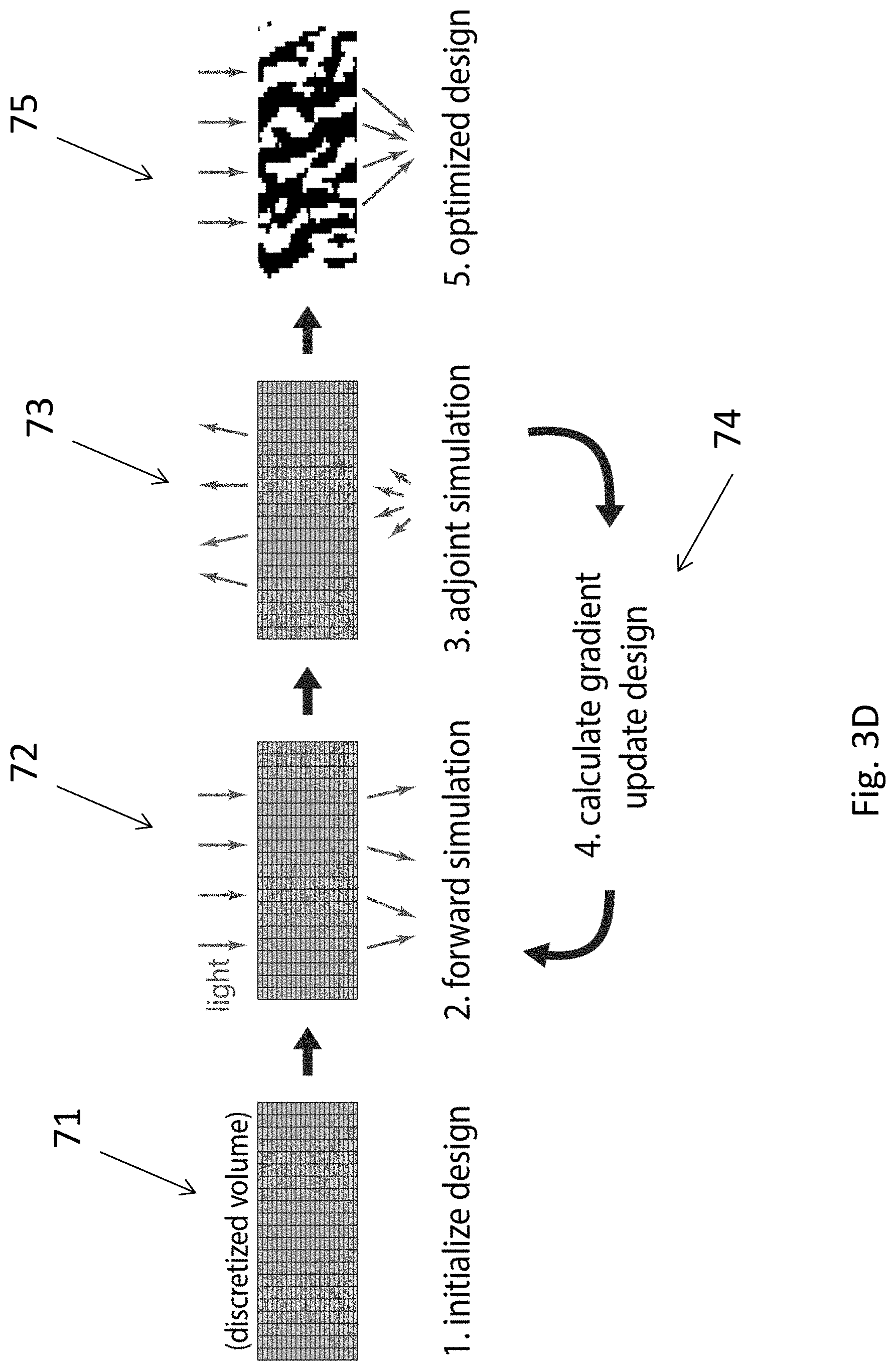
12. The method of claim 11, wherein the set size and pitch requirements are related to CMOS manufacturing constraints.
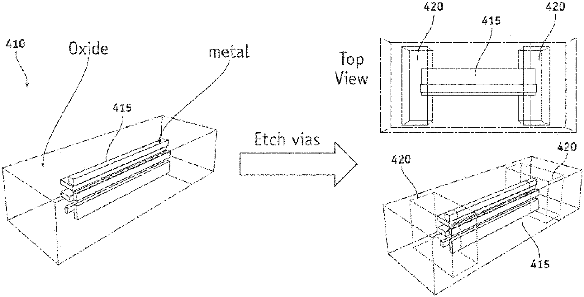
13. An image sensor built based on the method of claim 1.
Description
CROSS REFERENCE TO RELATED APPLICATIONS
[0001] The present application is related to U.S. patent application Ser. No. 16/656,156 filed on Oct. 17, 2019, titled "Color and Multi-Spectral Image Sensor Based On 3D Engineered Material" (Att. Docket No. P2404-US), the contents of which are incorporated herein by reference in their entirety.
FIELD
[0003] The presented disclosure is related to image sensors, and more particularly to metamaterial spectrum splitters manufactured using CMOS fabrication technology.
BACKGROUND
[0004] Optical systems are typically designed via modular combinations of elements to achieve complex functions. For example, lenses and diffractive optics can be combined to perform hyperspectral imaging. This approach is intuitive and flexible, providing access to a wide range of functions from a limited set of elements. However, the overall size and weight of the optical system may limit its scope of applications. Recent advancements in nanofabrication may alleviate this constraint by replacing bulky elements with metasurfaces--planar arrays of resonant nanostructures with sub-wavelength thickness. By engineering the scattering of individual elements within the array, these devices can reproduce the multi-functionality of complex optical systems in a single element. However, efforts to combine multiple metasurfaces for more complex functionality have been stymied by reduced scattering efficiency, which scales inversely with the number of simultaneous tasks.
[0005] The inherent trade-off between multi-functionality and efficiency in these systems is due to the finite number of degrees of freedom, which scales with the volume of the device and the maximum refractive index contrast. In particular, this limits the range of independent functions achievable by any ultrathin system, such as sorting light according to frequency, polarization, and incident angle. By contrast, three-dimensional scattering elements with thicknesses greater than a wavelength commonly encode many simultaneous functions, albeit so far only with low efficiency due to weak scattering and low index-contrast.
[0006] Historically, optical design has been modular, a paradigm that provides an intuitive way to build and reconfigure optical setups. With the advancement of nanofabrication technologies it became possible to make structures with sub-wavelength feature size that enabled multi-functional optical elements combining the functionality of more complex setups. Examples include metasurface lenses that can split different polarizations and spectral bands. However, the degree of performance and functionality that can be achieved with metasurfaces and other planar structures is inherently limited by the number of optical modes that can be controlled.
[0007] Structuring the refractive index with high contrast at sub-wavelength scale provides an expansive optical design space that can be harnessed for demonstrating multi-functional optical elements. So far this has been used mostly in two dimensional structures, or metasurfaces. However, their performance is limited by the available optical degrees of freedom.
[0008] In order to highlight the benefits of the teachings of the present disclosure in the following sections, the example of image sensors is considered here. Currently, the majority of sensors record color using absorptive filters. FIG. 1A shows a prior art image sensor, wherein each four neighboring pixels has an absorptive color filter on top: two are for green, one for blue and one for red. The issue with such an image sensor is that the efficiency is limited to around 30%, as most of the light is absorbed. Color image sensors are ubiquitous in cell phones, cameras and numerous kinds of instrumentation. The color is detected by simple absorptive filters placed directly on top of each pixel. The absorptive nature of the filters means that more than 2/3 of the light is actually lost by absorption, i.e. for example red and blue light incident on the green pixel is absorbed and only green passes through
SUMMARY
[0009] Complex three-dimensional (3D) scattering structures allowing, for example, the splitting of color on the Bayer pattern with higher efficiency are disclosed in the present application. Designs that provide polarization information are also described.
[0010] Cost-effective and large-scale fabrication of such structures poses significant challenges on the design process. The objective is to achieve the best performance given the inherent constraints associated with high-volume CMOS fabrication processes.
[0011] The disclosed methods and devices address the described challenges and provide practical solutions to the above-mentioned problem.
[0012] In particular, the disclosed methods and devices teach various steps to design 3D scattering structures using a scalable fabrication process. Currently, the most scalable fabrication that can handle dimensions smaller than 100 nm is the CMOS foundry fabrication process. In the CMOS process, it is possible to fabricate very complex networks of copper wires stacked on top of each other and embedded in SiO2. FIG. 1B shows an example of such networks, wherein light and dark gray represent metal and SiO2 respectively. However, according to an embodiment of the present disclosure, the wires can be etched away using liquid etchants so that the final 3D scattering structure is composed of voids in SiO2. In accordance with another embodiment of the present disclosure, the 3D scattering structure can be left as voids in SiO2, or the voids can be filled with higher refractive index materials like TiO2 using atomic layer deposition processes.
[0013] According to a first aspect of the present disclosure, a method for building a three-dimensional (3D) scattering structure is disclosed, comprising: forming a dielectric structure comprising a first dielectric and a network of metal wires, wherein location, shape and size of the metal wires are selected according to one or more target functions; and etching away the metal wires from the dielectric structure, thus forming a structure containing spaces filled with the first dielectric and voids, wherein location, shape and size of the voids is according to the one or more target functions, wherein the thus formed 3D light scattering structure is configured to receive electromagnetic waves and scatter the electromagnetic waves in accordance with the one or more target functions.
[0014] Further aspects of the disclosure are provided in the description, drawings and claims of the present application.
DESCRIPTION OF THE DRAWINGS
[0015] FIG. 1A shows a prior art image sensor.
[0016] FIG. 1B shows a prior art structure of wires that can be realized using CMOS foundry fabrication techniques, with feature sizes below 100 nm.
[0017] FIGS. 2A-2A' show exemplary three-dimensional (3D) scattering structures according to an embodiment of the present disclosure.
[0018] FIGS. 2B-2C show the wavelength splitting functionality of the embodiment of FIGS. 2A and 2A'.
[0019] FIGS. 3A-3C show an exemplary three-dimensional (3D) scattering structure according to another embodiment of the present disclosure.
[0020] FIG. 3D shows multiple steps of an exemplary optimization algorithm in accordance with an embodiment of the present disclosure.
[0021] FIG. 4A shows an exemplary 3D structure made of dielectric and comprising wire networks in accordance with an embodiment of the present disclosure.
[0022] FIG. 4B shows an exemplary process of etching away the wire network within a 3D structure, in accordance with a further embodiment of the present disclosure.
[0023] FIG. 5 shows an exemplary flowchart illustrating various steps of designing a 3D scattering structure in accordance with the teachings of the present disclosure.
[0024] FIG. 6 shows an exemplary graph illustrating the refractive index distribution along horizontal position.
[0025] FIGS. 7A-7C show graphs representing the performance of a 3D scattering structure implemented in accordance with the teachings of the present disclosure.
DETAILED DESCRIPTION
[0026] FIG. 2A shows an image sensor (200) according to an embodiment of the present disclosure. The image sensor (200) comprises a three-dimensional (3D) scattering structure (201) functioning as a spectrum splitter. The 3D scattering structure (201) comprises a plurality of dielectric pillars (205) formed to scatter light in a predefined pattern. Incident light (202) passing through the 3D scattering structure (201) is scattered off the dielectric pillars. Through arrangements of the dielectric pillars (205) in accordance with one or more target functions, the scattering pattern is tailored to perform a desired function. As an example, the 3D scattering structure (201) may be designed as a spectrum splitter to simultaneously sort and focus the incident light (202) into an arbitrary number of wavelengths (.lamda..sub.1, . . . , .lamda..sub.n) each directed to an individual pixel on a focal plane (203) placed underneath the 3D scattering structure (201), as shown in FIG. 2A. In accordance with embodiments of the present disclosure, the 3D scattering structure (201) may be a porous polymer cube or a cluster of dielectric or semiconductor (Si for example) particles embedded in a SiO2 matrix. According to further embodiments of the present disclosure, the 3D scattering structure (201) may be a porous polymer cube or a cluster of high-refractive index particles embedded in a low-refractive-index matrix.
[0027] The person skilled in the art will appreciate that, in contrast with the prior art image sensor (100) of FIG. 1A, the image sensor (200) of FIG. 2A, does not function based on absorption and as such, it provides a substantial improvement of efficiency compared to existing solutions. This will be quantified later using exemplary embodiments of the present teachings. As also described more in detail throughout the disclosure, the disclosed devices and methods provide the following additional benefits over existing solutions: [0028] The 3D scattering structure (201) of FIG. 2A may be manufactured through known and scalable lithographic processes. [0029] The 3D scattering structure (201) of FIG. 2A may be designed to function as a spectrum splitter for arbitrary spectral bands such as infrared, mid-infrared or alike. In other words, in addition to hyperspectral imaging, thermal imaging is another potential application of the disclosed teachings. [0030] The spectrum splitting function may be combined with other desired functions such as polarization splitting. [0031] Embodiments according to the present disclosure may also be designed to perform optical image processing such as Gabor filtering for edge detection.
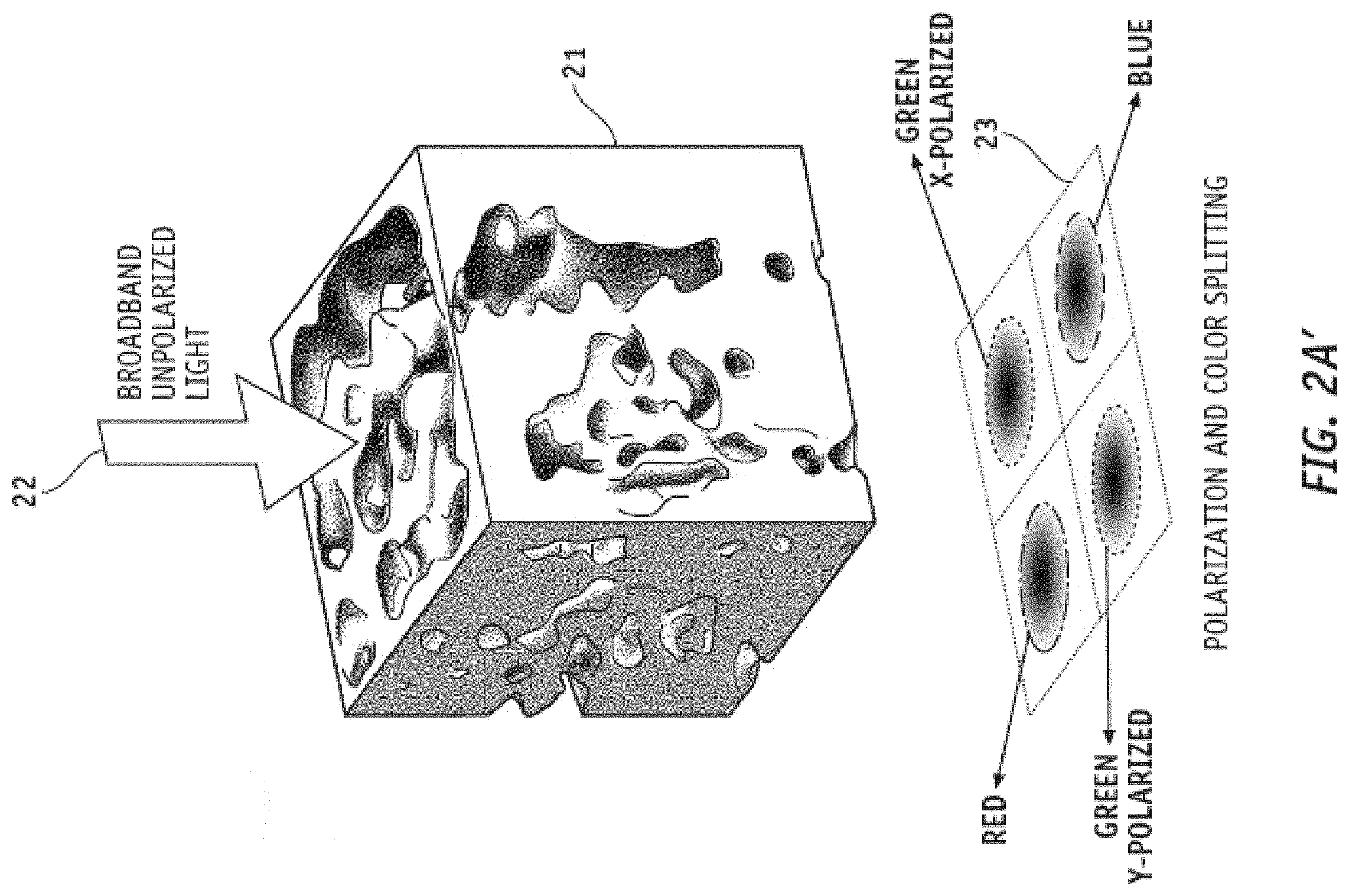
[0032] FIG. 2A' shows an image sensor (200') comprising an exemplary three-dimensional (3D) scattering structure (21) functioning as a spectrum filter, according to an embodiment of the present disclosure. Incident light (22) entering from the above is scattered while passing through the 3D scattering structure (21) and sorted in a focal plane (23) consisting of four sub-pixels, shown as red, blue, green (x-polarized) and green (y-polarized). As also shown in FIG. 2A', the red (600 nm-700 nm) and blue (400 nm-500 nm) spectral bands are sorted into opposite quadrants. Moreover, the green (500 nm-600 nm) spectral band is further split according to linear polarization. The red and blue quadrants may be polarization independent.
[0033] In accordance with embodiments of the present disclosure, the 3D scattering structure (21) may be designed using an adjoint variable method, which generates a structure that optimizes a specified objective function. As an example, and referring to FIG. 2A', the objective function may be selected based on the focusing efficiency of incident light into one of four target areas depending on the frequency and polarization. Starting with an empty volume, full-wave finite-difference time-domain (FDTD) simulations are implemented to calculate the sensitivity of this figure of merit to perturbations of the refractive index. The prescribed scattering structure is formed and updated iteratively. In other words, the optimal design is generated through iterative updates to an initial geometry, each step improving the performance. The sensitivity may be calculated from just two simulations, allowing efficient optimization of 3D devices with modest resources. The sensitivity for multiple incident wavelengths across the visible spectrum may be calculated, to assign each spectral band to a different quadrant: red (600 nm-700 nm) green (500 nm-600 nm) and blue (400 nm-500 nm). Then a spectrally-averaged sensitivity may be used to update the refractive index of the device.
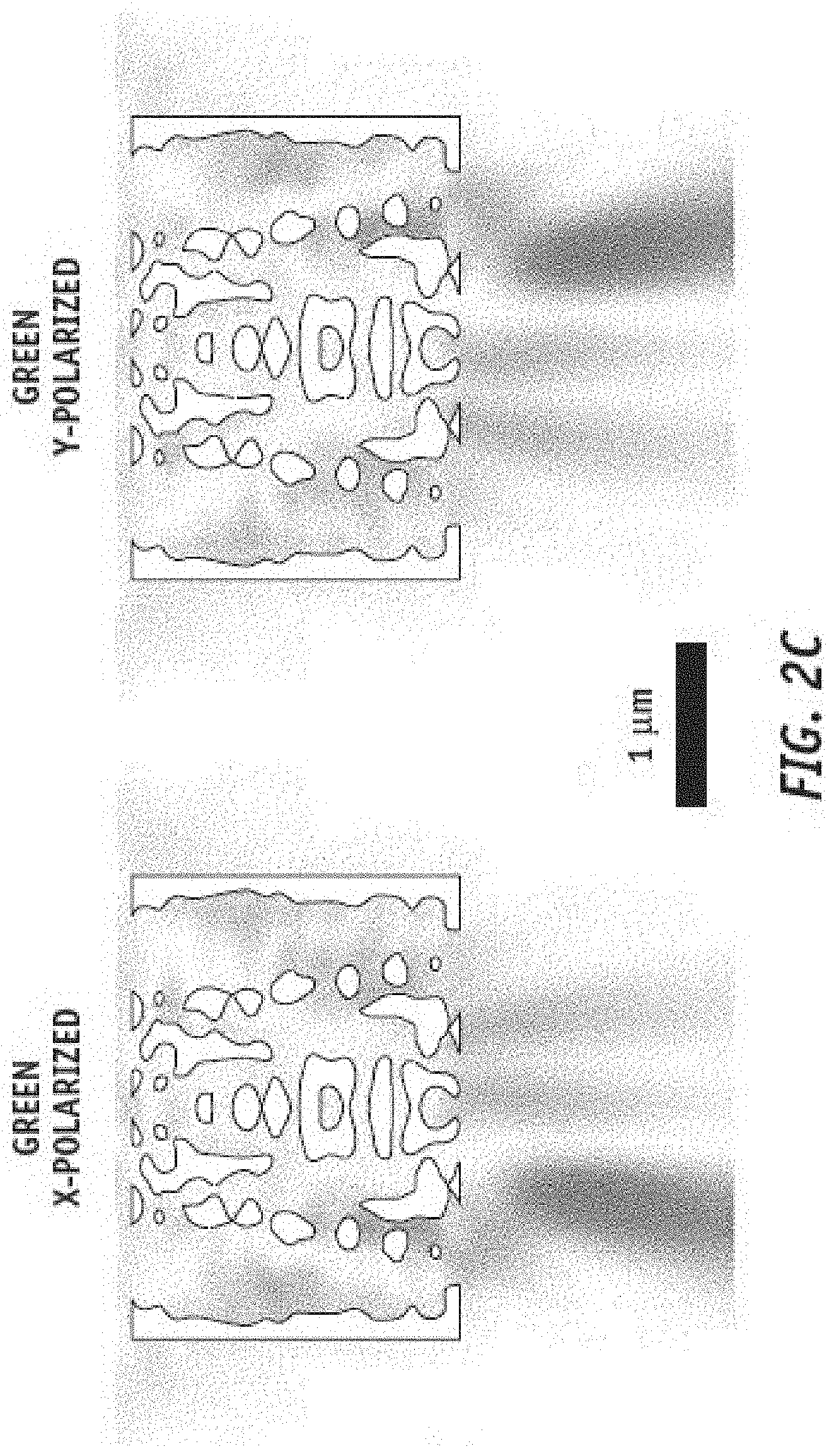
[0034] FIGS. 2B-2C show the simulated intensity of the incident light within the 3D scattering structure (21) of FIG. 2A'. The intensity is analyzed along a diagonal cross section that intersects the red and blue quadrants of FIG. 2A'. Each wavelength undergoes multiple scattering before focusing to its respective target region. FIG. 2C shows the intensity distribution of incident light within a diagonal cross-section through the green pixels for two orthogonal input polarizations. In both cases, a plane wave (.lamda.=550 nm) incident from above is preferentially routed to the pixel corresponding to its polarization. Meanwhile, both polarizations are assigned the same region for red and blue spectral bands, maintaining the mirror symmetry of the objective function.
[0035] In accordance with an embodiment of the present disclosure, the 3D scattering structure (21) of FIG. 2A' sorts red, green, and blue light with 84%, 60% and 87% efficiency respectively. Throughout the present disclosure, the efficiency is defined as the fraction of the total power incident on the device that reaches the target quadrant averaging across the spectrum for which the device is designed for, i.e. the visible spectrum for the embodiment of FIG. 2A'.
[0036] With reference to FIGS. 2A, and 2A', the person skilled in the art will appreciate that the disclosed concept provides substantial flexibility in defining the target scattering function, with independent control for any incident polarization, angle, or frequency. However, complex three-dimensional structures present a significant challenge for fabrication. Large-scale implementation of these devices in image sensors at visible wavelengths will require high fabrication throughput with sub-100-nm resolution. This may be achieved by multi-layer lithography, where three-dimensional devices are constructed through repeated material deposition and patterning. Here, each layer consists of a series of patterned mesas composed of a high-index dielectric. The interstitial space is filled with a low-index dielectric, forming a flat surface that serves as a substrate for subsequent layers.
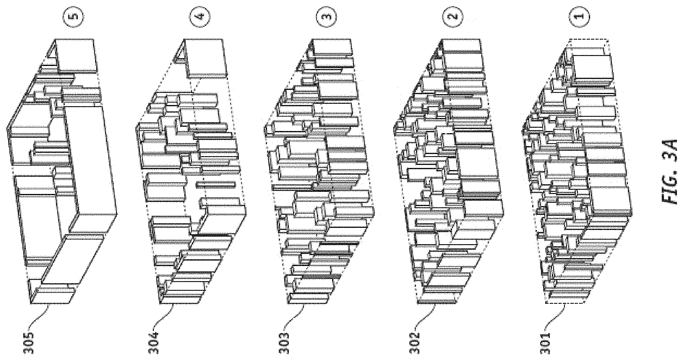
[0037] In order to further clarify the layered manufacturing approach discussed above, reference is made to FIGS. 3A and 3C illustrating a layered design of a 3D scattering structure (31) of FIG. 3C. In other words, the 3D scattering structure (31) of FIG. 3C may be structured by stacking the plural layers (301, . . . , 305) of FIG. 3A on top of one another. The fabrication process may be CMOS-compatible wherein the fabrication constraints may be directly incorporated with the design algorithm. Each layer (301, . . . , 305) may be produced using lithography. The 3D scattering structure (31) may be composed of TiO2 and SiO2, materials that are transparent at visible frequencies. The layers (301, . . . , 305) may be 2 um.times.2 um layers, each 400 nm tall. The person skilled in the art will understand that these are exemplary dimensions for description purposes, and that embodiments in accordance with the present disclosure, and with dimensions and numbers of layers other than those mentioned above may also be envisaged. As shown in FIG. 3B, each layer may comprise a set of irregular TiO2 mesas surrounded by SiO2. With reference to FIG. 3B', the lithography process may begin by growing a thin layer of dielectric (e.g. TiO2) on top of a substrate (e.g. SiO2). A pattern is transferred onto this layer by lithography and the unprotected material is etched away to produce a two-dimensional dielectric structure. Finally, the surface is coated (deposition) with low-refractive index dielectric and mechanically polished (planarization). By repeating the same process for each layer and stacking up layers the desired 3D structure is produced. Such a lithography process provides flexibility in material design, and is compatible with industry-standard CMOS fabrication process, as noted above.
Optimization Algorithms
Gradient Descent
[0038] Referring back to FIGS. 2A'-3C, and as mentioned previously, three-dimensional dielectric structures, optimized to perform a target optical scattering function are designed according to the teachings of the disclosure. In the case of the exemplary embodiments shown in FIGS. 2A'-3C, such target scattering function consists of focusing incident plane waves to different positions depending on the frequency and polarization. The exemplary three-dimensional (3D) scattering structures (21, 31) are defined by a spatially-dependent refractive index distribution n({right arrow over (x)}) within a cubic design region. This represents an expansive design space with the capacity to express a broad range of complex optical multi-functionality. However, identifying the optimal index distribution for a given target function remains a challenging inverse design problem, particularly for strongly scattering devices.
[0039] In order to overcome such a challenge, and according to the teachings of the present disclosure, an iterative approach guided by gradient descent may be implemented, wherein starting from an initial index distribution, full-wave simulations (FDTD) is used to calculate the sensitivity of the focusing efficiency with respect to perturbations of the refractive index. The sensitivity may be calculated from just two simulations, allowing efficient optimization of three-dimensional devices with modest resources. Based on the sensitivity, the initial design is modified in order to maximize the performance while conforming to fabrication constraints. This update process is repeated until the optimized device can efficiently perform the target function
[0040] In order to further clarify what is described above, reference is made to FIG. 3D showing multiple steps of a gradient based optimization algorithm in accordance with an embodiment of the present disclosure. The algorithm is initialized, step (81), with a uniform refractive index distribution,
n 0 ( x .fwdarw. ) = n max + n min 2 , ##EQU00001##
wherein n.sub.max and n.sub.min represent the maximum and minimum values of the refractive index respectively. This distribution is continually updated to maximize the electromagnetic intensity at the target location in focal plane, f (n({right arrow over (x)}))=|{right arrow over (E)}({right arrow over (x)}.sub.0)|.sup.2. This objective function serves as a proxy for focusing efficiency while simplifying the sensitivity calculation. The sensitivity,
df dn ( x .fwdarw. ) , ##EQU00002##
is computed, step 74, from the electromagnetic fields in two FDTD simulations (forward and adjoint), steps (72, 73), according to the following expression:
df dn ( x .fwdarw. ) = 2 n ( x .fwdarw. ) Re { E .fwdarw. fwd E .fwdarw. adj } ( 1 ) ##EQU00003##
where {right arrow over (E)}.sub.fwd are the electric fields within the cube when illuminated from above with a plane wave, step (72), and {right arrow over (E)}.sub.adj are the electric fields within the cube when illuminated from below, step (73) with a point source at the target location. The phase and amplitude of the point source are given by the electric field at the target location in the forward simulation. The sensitivity may be calculated for multiple incident wavelengths and polarizations across the visible spectrum, assigning each spectral band to a different quadrant: red (600 nm-700 nm) green (500 nm-600 nm) and blue (400 nm-500 nm). The spectrally-averaged sensitivity is then used to update the refractive index of the device, step (74), using the following formula:
n i + 1 ( x .fwdarw. ) = n i ( x .fwdarw. ) + .alpha. .SIGMA. .lamda. d f .lamda. d n ( x .fwdarw. ) ( 2 ) ##EQU00004##
The step size .alpha. may be fixed at a small fraction (e.g., .alpha.=0.001) to ensure that the change in refractive index can be treated as a perturbation in the linear regime. The sensitivity is recalculated after each update. After several iterations, the algorithm converges to the optimized design, step (75), wherein the resulting structure focuses incident light with the desired efficiency.
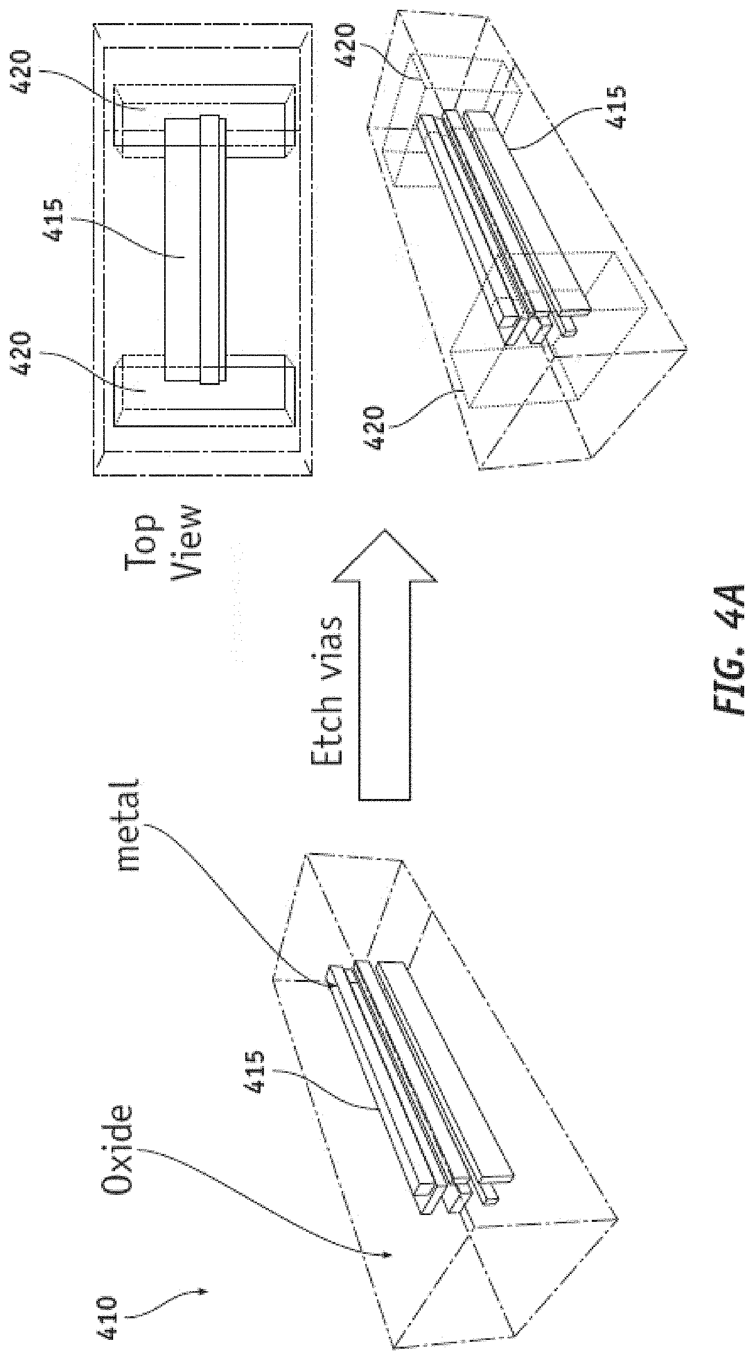
[0041] FIG. 4A shows a 3D scattering structure (410) made of a dielectric, the 3D structure (410) comprising a wire network (415) embedded inside the scattering structure (410). The dielectric may be made of an oxide such as SiO2 and the wire network (415) may be made of metal, e.g. copper. As mentioned previously, in order to produce complex 3D scattering elements performing a target function, voids may be formed within the 3D structure (410) by etching away the wire network (415) initially fabricated within the 3D scattering structure (410). In order to do this, making now reference to FIGS. 4A-4B, and according to further embodiments of the present disclosure, vias (420) are etched in the dielectric to access ends of wires in the wire network (405) and then etching the wires away using a liquid etchant, in order to obtain voids (415').
[0042] Throughout the disclosure, the term "wire pitch" will be referred to the minimum spacing two neighboring wires of a wire network within a 3D structure can be from each other. Also, there is a minimum wire feature size imposed by limitations of the fabrication process. Therefore, when forming voids within the 3D structure by etching out wires, the minimum wire pitch sets the minimum dielectric feature size and the minimum wire size sets the minimum void/air feature size. In what follows, exemplary steps of the methods in accordance with the teaching of the present disclosure to design the 3D scattering structure (410) while respecting manufacturing process constraints are described.
Free, Continuous Optimization
[0043] In what follows, 3D structures made of a dielectric wherein voids are formed in accordance with a target function will be described. The process may start with a free optimization, as described in the previous sections with regards to FIGS. 2A-3D, where the index of refraction is allowed to change continuously between air (n=1.0) and a low index material, SiO2 (n=1.5). As an example, a gradient descent algorithm may be used where the sensitivity of an objective function to changes in the index is calculated at all points in the design region. With reference to the example of FIGS. 2A' and 3C, the objective function to be optimized may be selected as an electric field intensity at different focal points for different wavelength bands. Such an objective function may be used when a wavelength splitter is being designed. The design obtained by the free and continuous optimization may not be in-line with requirements imposed by constraints due to manufacturing. Throughout this document, the term "free optimization" refers to optimization methods wherein no fabrication constraints are imposed and the term "continuous optimization" refers to optimization methods wherein a specific fabrication constraint is lifted. As an example, in such optimization methods, the refractive index can take any value within a set range, not just the extremes. As detailed in the following paragraphs, the disclosed methods address this issue by implementing a binarization of the refractive index followed by further optimization of the design using, for example, a gradient descent approach, while respecting the manufacturing requirements.
Two Dimensional (2D) Shape Representation and Binarization
[0044] Throughout this document, the term "binarization" refers to a fabrication constraint wherein only a handful of materials can be selected, so no continuous index distribution is allowed. As an example, the CMOS technology imposes such a fabrication constraint. Considering the example of a 2D shape, an explicit representation of such a shape may be a series of points in a 2D plane that define the boundary of such shape. In case of a rectangle, the shape can be defined by just four points in the plane. Another way of representing either specific shapes like rectangles or arbitrary shapes is to use an implicit representation. Throughout this document, the term "level set function" is referred to a function that is an implicit representation of a geometry. For example, in the case of a 2D shape, a level set function may be defined as a function f(x, y), or in other words a surface in three dimensions. The contour defined by f(x, y)=constant (e.g., the constant is equal to 0) defines the boundary of the shape in two dimensions.
[0045] As will be detailed later, in accordance with embodiments of the present disclosure, level set functions representing features with geometric shapes such as rectangle instead of free form shapes as allowed by the free, continuous optimization algorithm may be envisaged. As described later, this approach will allow an optimized design while tight requirements imposed by the manufacturing process are met. The gradient information from the continuous optimization method can then be mapped to perturbations of the level set function such that the boundary of the shape moves in a way to improve the design. When simplifying to features with, for example, rectangular shape (or some other parameterizable shape), this boundary perturbation can be converted to a perturbation of the feature parameters, e.g., in the case of a rectangle, a center point and two widths. In what follows, the example of features with rectangular shapes will be used to describe the teachings of the disclosure, keeping in mind that features with shapes other than rectangular may also be envisaged.
Level Set Representation
[0046] According to embodiments of the present disclosure, the design of 3D structures mentioned previously is implemented in 2D while enforcing a layering in the direction of propagation of the input source. In other words, making for example reference to rectangular features, the position and the width of the features are the parameters that are controlled. FIG. 5 shows a flowchart (500) describing various steps of the design process, in accordance with embodiments of the present disclosure. As can be seen in the flowchart (500), first an initial optimized design based on free/continuous optimization is provided (step 510). This design will essentially provide the refractive index distribution along horizontal directions in each layer and no manufacturing constraint is imposed when generating such initial design. Then for each layer, the following steps are taken:
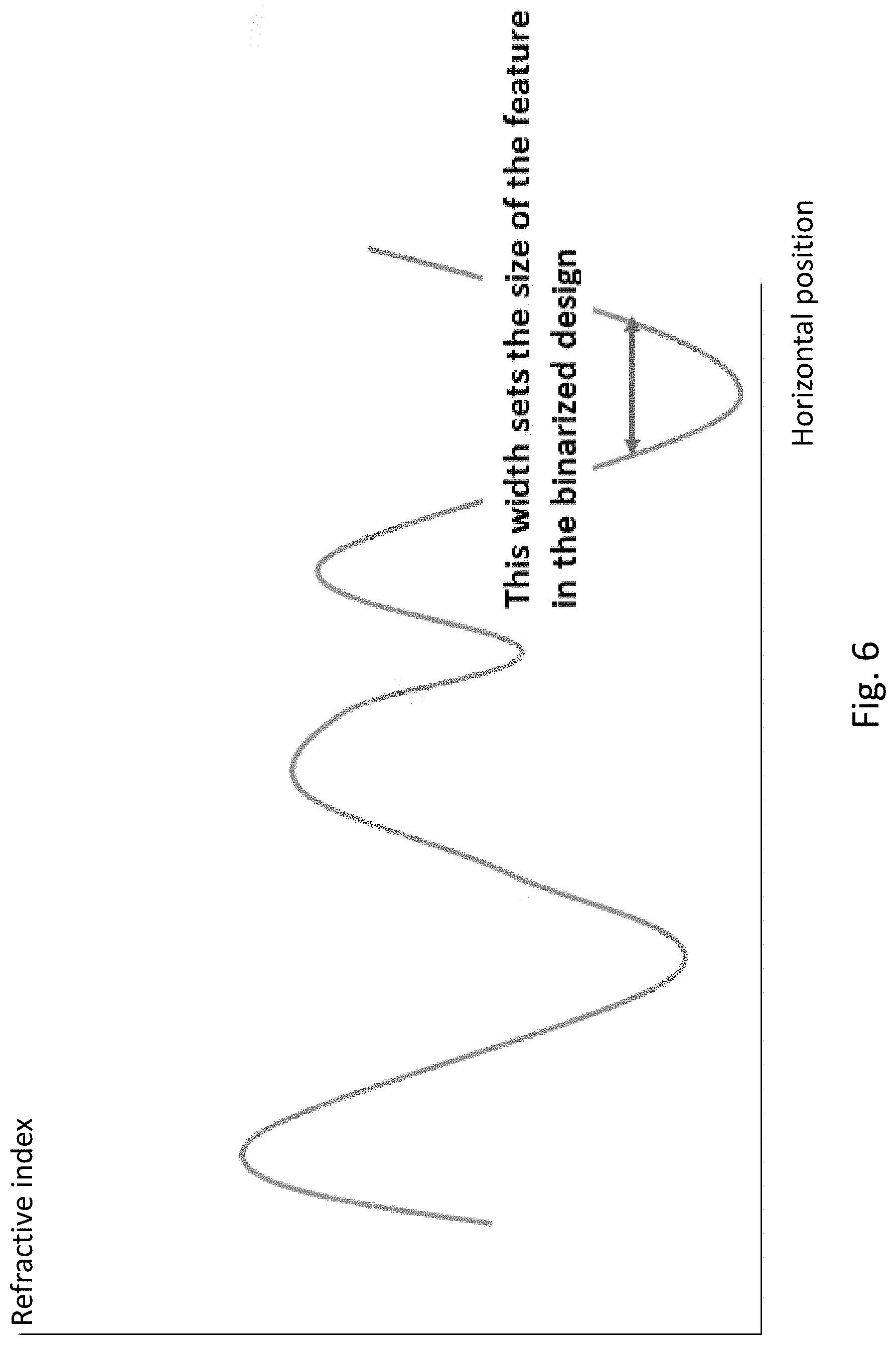
1. A procedure is run to identify peaks in the void index distribution (step 520). The minima found in this way represent void regions that may not necessarily be completely void according to the free/continuous optimization as previously described. In other words, some regions may represent local minima. 2. The identified regions are then ranked based on how close they are to being a void (step 530). This is performed using the outcome of the design based on the free/continuous optimization algorithm as described previously. In other words, void features are prioritized to be placed where they seem to be most desired by the free design. 3. Proceeding from the highest to the lowest ranked void features, each void is replaced with a rectangle that approximates the original index distribution (step 540). The dimensions of the rectangle are chosen to maintain the same volume-averaged refractive index as the original distribution, providing a binary-index replacement. This is illustrated in FIG. 6 wherein an exemplary graph representing the index distribution vs. the horizontal position is shown. 4. The manufacturing (e.g. CMOS process) constraints are required to be met by each feature (steps 550-570). In other words, the width of each feature is required to meet the minimum width requirement, which is set, as mentioned before, by the minimum wire size that is manufacturable. The distances between centers of adjacent features are required to meet the manufacturing pitch requirement. Any feature not meeting any of such requirements may be ignored. 5. Using the center/width of each feature as found in the previous steps, a level set function is created and assigned to each feature (step 580). As described later, the created level functions will be updated (step 580) to improve the performance of the binarized design.
Performance Improvement of the Binarized Design
[0047] As mentioned previously, according to embodiments of the present disclosure, and in order to meet manufacturing constraints, the 3D structures may be designed based on specific shapes such as rectangular bars. As typical from designs using free/continuous optimization, such designs already provide improved overall performance compared to existing solutions. However, designing based on freeform shapes may still result in a better overall performance compared to those based on more specific features. In accordance with the teachings of the disclosure, and starting from a binarized device, the gradient information can be used to iteratively update the design to further improve the overall performance. As illustrated by flowchart (500) of FIG. 5, step (580), the gradient information from the free/continuous optimization method can be mapped to perturbations of the width/center of all rectangular features used in the binarized design (step 580 of FIG. 5). In other words, the gradient of the objective function with respect to the index distribution can be mapped to a perturbation of the boundaries via the Hamilton-Jacobi equation. This means we can update the boundary (here widths) using the same information that is used to optimize the continuous graded-index structure. The inventors have noticed that, when adopting such an approach, and after several iterations, significant improvement over the already good performance of the binarized design will be obtained, while respecting at the same time the constraints imposed by the manufacturing process (e.g. CMOS process). In what follows, the performance of the described design approach will be described using exemplary embodiments of the disclosure.
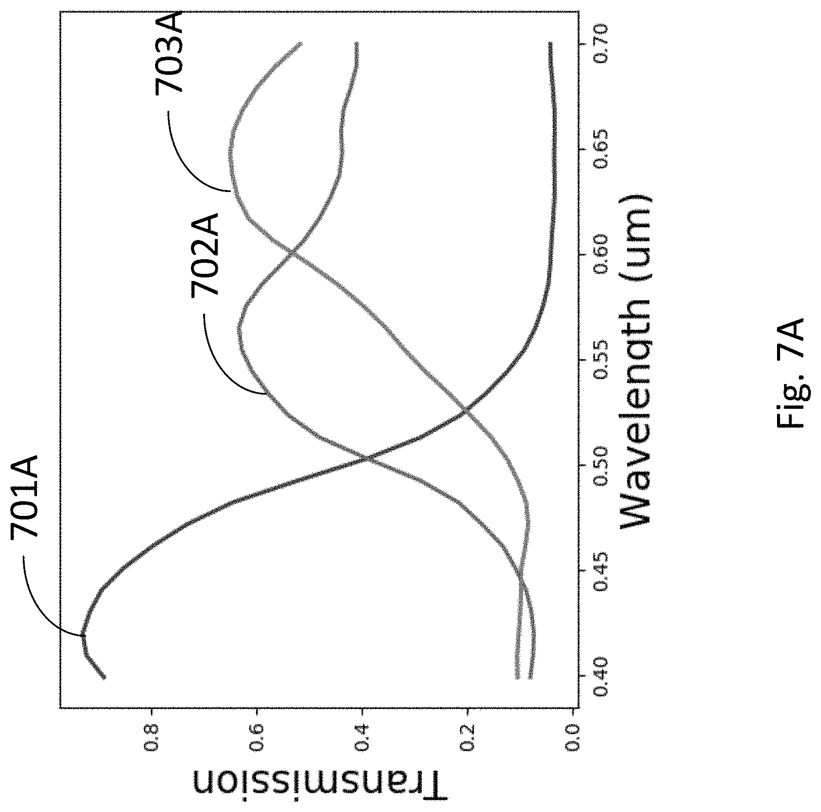
[0048] FIGS. 7A-7C show performance results related to an exemplary 3D scattering structure optimized for single polarization and 3 color focus (e.g. red, green and blue). The 3D structure is made of SiCOH (n=1.3) wherein air gaps (n=1) are formed using the methods described previously. A 2D approach as described before was used using 8 layers (450 nm/layer). FIG. 7A shows the transmission spectra related to the design based on free/continuous optimization. Graphs (701A, 702A, 703A) represent plots of transmission as a function of wavelength for colors (blue, green, red) respectively. FIG. 7B shows the transmission spectra related to the binarized design. Graphs (701B, 702B, 703B) represent plots of transmission as a function of wavelength for different focal regions. A degradation of the performance compared to the results obtained in the case of free optimization is noticed. FIG. 7C shows the transmission spectra obtained after further optimizing the binarized design after the gradient information from the free/continuous optimization method is mapped to perturbations of the width/center of all of the rectangular features used in the binarized design. Graphs (701C, 702C, 703C) represent plots of transmission as a function of wavelength for colors (blue, green, red) respectively. A significant improvement over the performance of the binarized design can be noticed.
* * * * *
D00000
D00001
D00002
D00003
D00004
D00005
D00006
D00007
D00008
D00009
D00010
D00011
D00012

D00013

D00014
D00015
D00016

D00017


XML
uspto.report is an independent third-party trademark research tool that is not affiliated, endorsed, or sponsored by the United States Patent and Trademark Office (USPTO) or any other governmental organization. The information provided by uspto.report is based on publicly available data at the time of writing and is intended for informational purposes only.
While we strive to provide accurate and up-to-date information, we do not guarantee the accuracy, completeness, reliability, or suitability of the information displayed on this site. The use of this site is at your own risk. Any reliance you place on such information is therefore strictly at your own risk.
All official trademark data, including owner information, should be verified by visiting the official USPTO website at www.uspto.gov. This site is not intended to replace professional legal advice and should not be used as a substitute for consulting with a legal professional who is knowledgeable about trademark law.