Apparatus And Methods For Selectively Etching Films
Wang; Fei ; et al.
U.S. patent application number 17/070580 was filed with the patent office on 2021-04-22 for apparatus and methods for selectively etching films. The applicant listed for this patent is ASM IP Holding B.V.. Invention is credited to Aditya Walimbe, Fei Wang.
| Application Number | 20210118687 17/070580 |
| Document ID | / |
| Family ID | 1000005195372 |
| Filed Date | 2021-04-22 |


| United States Patent Application | 20210118687 |
| Kind Code | A1 |
| Wang; Fei ; et al. | April 22, 2021 |
APPARATUS AND METHODS FOR SELECTIVELY ETCHING FILMS
Abstract
An apparatus and methods for selectively etching a particular layer are disclosed. The apparatus and methods are directed towards maintaining the etch rate of the particular layer, while keeping intact a non-etched layer. The etching process may be accomplished by co-flowing a hydrogen precursor gas and a fluorine precursor gas into a remote plasma unit. A resulting gas mixture may then be flowed onto the substrate having a silicon oxide layer as an etch layer and a silicon nitride layer as a non-etched layer, for example. A reaction between the resulting gas mixture and the particular layer takes place, resulting in etching of the silicon oxide layer while maintaining the silicon nitride layer in the above example.
| Inventors: | Wang; Fei; (Tempe, AZ) ; Walimbe; Aditya; (Tempe, AZ) | ||||||||||
| Applicant: |
|
||||||||||
|---|---|---|---|---|---|---|---|---|---|---|---|
| Family ID: | 1000005195372 | ||||||||||
| Appl. No.: | 17/070580 | ||||||||||
| Filed: | October 14, 2020 |
Related U.S. Patent Documents
| Application Number | Filing Date | Patent Number | ||
|---|---|---|---|---|
| 62923958 | Oct 21, 2019 | |||
| Current U.S. Class: | 1/1 |
| Current CPC Class: | H01L 21/67069 20130101; H01L 21/02046 20130101; H01L 21/3065 20130101; H01J 37/3244 20130101 |
| International Class: | H01L 21/3065 20060101 H01L021/3065; H01J 37/32 20060101 H01J037/32; H01L 21/67 20060101 H01L021/67; H01L 21/02 20060101 H01L021/02 |
Claims
1. A method for selectively etching a film disposed on a substrate, the method comprising: providing a substrate in a reaction chamber of a semiconductor processing device, the substrate having a first layer and a second layer; igniting a plasma in a remote plasma unit by flowing an inert gas into the remote plasma unit; flowing a hydrogen precursor gas and a fluorine precursor gas concurrently as a gaseous mixture into the remote plasma unit; flowing the gaseous mixture onto the substrate, whereby a reaction takes place between the gaseous mixture and the first layer, resulting in an etching of the first layer while maintaining intact the second layer; wherein the fluorine precursor gas comprises at least one of: nitrogen trifluoride (NF.sub.3); carbon tetrafluoride (CF.sub.4); sulfur hexafluoride (SF.sub.6); hydrogen fluoride (HF); hydrofluoric acid (HF) with water vapor; or fluorine (F.sub.2); and wherein the hydrogen precursor gas comprises at least one of: hydrogen (H.sub.2); hydrogen fluoride (HF); hydrogen chloride (HCl); or water (H.sub.2O).
2. The method of claim 1, further comprising: flowing an ammonia precursor gas into the reaction chamber, whereby the ammonia precursor gas mixes with the gaseous mixture.
3. The method of claim 2, wherein the ammonia precursor gas comprises at least one of: ammonia (NH.sub.3); hydrazine (N.sub.2H.sub.4); or urea (NH.sub.2CONH.sub.2).
4. The method of claim 1, further comprising: flowing the hydrogen precursor gas by itself into the remote plasma unit before flowing a hydrogen precursor gas and a fluorine precursor gas concurrently.
5. The method of claim 1, further comprising: flowing the fluorine precursor gas by itself into the remote plasma unit before flowing a hydrogen precursor gas and a fluorine precursor gas concurrently.
6. The method of claim 1, wherein the first layer comprises at least one of: silicon oxide; germanium oxide; aluminum oxide; cobalt oxide; tungsten oxide; silicon; germanium; aluminum; cobalt; tungsten; or alloys of various metals.
7. The method of claim 1, wherein the second layer comprises at least one of: silicon nitride; metal nitride; or aluminum nitride.
8. The method of claim 1, wherein the inert gas comprises at least one of: argon; krypton; helium; xenon; or nitrogen.
9. A system for selectively etching a film disposed on a substrate, the system comprising: a reaction chamber configured to hold and process a substrate, the substrate having a first layer and a second layer; a remote plasma unit coupled to the reaction chamber; a fluorine precursor gas source configured to provide a fluorine precursor gas to the remote plasma unit, the fluorine precursor gas comprising at least one of: nitrogen trifluoride (NF.sub.3); carbon tetrafluoride (CF.sub.4); sulfur hexafluoride (SF.sub.6); hydrogen fluoride (HF); hydrofluoric acid (HF) with water vapor; or fluorine (F.sub.2); a hydrogen precursor gas source configured to provide a hydrogen precursor gas to the remote plasma unit, the hydrogen precursor gas comprising at least one of: hydrogen precursor gas comprises at least one of: hydrogen (H.sub.2); hydrogen fluoride (HF); hydrogen chloride (HCl); or water (H.sub.2O); and an inert gas source configured to provide an inert gas to the remote plasma unit, wherein the inert gas is ignited to form a plasma in the remote plasma unit; wherein the remote plasma unit is configured to receive a co-flow of the fluorine precursor gas and the hydrogen precursor gas; and wherein the gaseous mixture is flowed onto the substrate, resulting in an etching of the first layer while maintaining intact the second layer.
10. The system of claim 9, further comprising: an ammonia precursor gas source configured to provide an ammonia precursor gas to the reaction chamber.
11. The system of claim 10, wherein the ammonia precursor gas comprises at least one of: ammonia (NH.sub.3); hydrazine (N.sub.2H.sub.4); or urea (NH.sub.2CONH.sub.2).
12. The system of claim 9, wherein the first layer comprises at least one of: silicon oxide; germanium oxide; aluminum oxide; cobalt oxide; tungsten oxide; silicon; germanium; aluminum; cobalt; tungsten; or alloys of various metals.
13. The system of claim 9, wherein the second layer comprises at least one of: silicon nitride; metal nitride; or aluminum nitride.
14. The system of claim 9, wherein the inert gas comprises at least one of: argon; krypton; helium; xenon; or nitrogen.
Description
CROSS-REFERENCE TO RELATED APPLICATIONS
[0001] This application is a Nonprovisional of, and claims priority to and the benefit of, U.S. Provisional Patent Application No. 62/923,958, filed on Oct. 21, 2019 and entitled "APPARATUS AND METHODS FOR SELECTIVELY ETCHING FILMS," which is hereby incorporated by reference herein.
FIELD OF INVENTION
[0002] The present disclosure generally relates to an apparatus for processing semiconductor wafers. More particularly, the disclosure relates to an apparatus and methods for selectively etching a particular film on a semiconductor wafer prior to additional processing.
BACKGROUND OF THE DISCLOSURE
[0003] During formation of semiconductor devices, there is a significant likelihood that multiple films would be formed. For example, metal oxides and silicon oxides may be formed during deposition of several films to form a NMOS or PMOS device. In certain applications, removal of the metal oxides and silicon oxides may be needed before deposition of additional films takes place.
[0004] Removal of the metal oxides and silicon oxides may be accomplished through the flow of particular chemistries as described in U.S. Pat. No. 9,514,927, entitled "Plasma Pre-Clean Module and Process" and which is hereby incorporated by reference. Certain chemistries may result in etching of additional films besides the metal oxide and silicon oxide films. The etching of additional films is undesirable as the additional films may be needed for the formation of the eventual semiconductor device.
[0005] As a result, an apparatus and methods that exhibit selectivity for etching one particular film over another are desired.
SUMMARY OF THE DISCLOSURE
[0006] In accordance with at least one embodiment of the invention, a method for selectively etching a film (e.g., a film used in the formation of semiconductor devices) disposed on a substrate is disclosed. The method may comprise: providing a substrate in a reaction chamber of a semiconductor processing device, the substrate having a first layer and a second layer; igniting a plasma in a remote plasma unit by flowing an inert gas into the remote plasma unit; flowing a hydrogen precursor gas and a fluorine precursor gas concurrently as a gaseous mixture into the remote plasma unit; flowing the gaseous mixture onto the substrate, whereby a reaction takes place between the gaseous mixture and the first layer, resulting in an etching of the first layer while maintaining intact the second layer; wherein the fluorine precursor gas comprises at least one of: nitrogen trifluoride (NF.sub.3); carbon tetrafluoride (CF.sub.4); sulfur hexafluoride (SF.sub.6); hydrogen fluoride (HF); hydrofluoric acid (HF) with water vapor; or fluorine (F.sub.2); and wherein the hydrogen precursor gas comprises at least one of: hydrogen (H.sub.2); hydrogen fluoride (HF); hydrogen chloride (HCl); or water (H.sub.2O).
[0007] In accordance with at least one embodiment of the invention, a system for selectively etching a film disposed on a substrate is disclosed. The system comprises: a reaction chamber configured to hold and process a substrate, the substrate having a first layer and a second layer; a remote plasma unit coupled to the reaction chamber; a fluorine precursor gas source configured to provide a fluorine precursor gas to the remote plasma unit, the fluorine precursor gas comprising at least one of: nitrogen trifluoride (NF.sub.3); carbon tetrafluoride (CF.sub.4); sulfur hexafluoride (SF.sub.6); hydrogen fluoride (HF); hydrofluoric acid (HF) with water vapor; or fluorine (F.sub.2); a hydrogen precursor gas source configured to provide a hydrogen precursor gas to the remote plasma unit, the hydrogen precursor gas comprising at least one of: hydrogen precursor gas comprises at least one of: hydrogen (H.sub.2); hydrogen fluoride (HF); hydrogen chloride (HCl); or water (H.sub.2O); and an inert gas source configured to provide an inert gas to the remote plasma unit, wherein the inert gas is ignited to form a plasma in the remote plasma unit; wherein the remote plasma unit is configured to receive a co-flow of the fluorine precursor gas and the hydrogen precursor gas; wherein the remote plasma unit is configured to mix the nitrogen precursor gas with the fluorine precursor gas and the hydrogen precursor gas to form a gaseous mixture; and wherein the gaseous mixture is flowed onto the substrate, resulting in an etching of the first layer while maintaining intact the second layer.
[0008] This summary is provided to introduce a selection of concepts in a simplified form. These concepts are described in further detail in the detailed description of example embodiments of the disclosure below. This summary is not intended to identify key features or essential features of the claimed subject matter, nor is it intended to be used to limit the scope of the claimed subject matter.
BRIEF DESCRIPTION OF THE DRAWING FIGURES
[0009] These and other features, aspects, and advantages of the invention disclosed herein are described below with reference to the drawings of certain embodiments, which are intended to illustrate and not to limit the invention.
[0010] FIGS. 1A and 1B are cross-sectional illustrations of a semiconductor device in accordance with at least one embodiment of the invention.
[0011] FIGS. 2A-2D are flowcharts of methods for selectively etching a film in accordance with at least one embodiment of the invention.
[0012] FIG. 3 is a schematic illustration of a semiconductor processing system in accordance with at least one embodiment of the invention.
[0013] It will be appreciated that elements in the figures are illustrated for simplicity and clarity and have not necessarily been drawn to scale. For example, the dimensions of some of the elements in the figures may be exaggerated relative to other elements to help improve understanding of illustrated embodiments of the present disclosure.
DETAILED DESCRIPTION OF EXEMPLARY EMBODIMENTS
[0014] Although certain embodiments and examples are disclosed below, it will be understood by those in the art that the invention extends beyond the specifically disclosed embodiments and/or uses of the invention and obvious modifications and equivalents thereof. Thus, it is intended that the scope of the invention disclosed should not be limited by the particular disclosed embodiments described below.
[0015] The illustrations presented herein are not meant to be actual views of any particular material, structure, or device, but are merely idealized representations that are used to describe embodiments of the disclosure.
[0016] Various embodiments are related to a cleaning process for removing a silicon oxide, a germanium oxide, or a metal oxide material from an exposed surface of a substrate. The embodiments may also be used to remove at least one of: silicon; metals in its elemental form; alloys of various metals; oxides related to the alloys of various metals; silicon; or germanium. It may be understood that a resulting cleaned surface will allow for formation of high quality semiconductor layers, such as epitaxially grown silicon, for example.
[0017] FIG. 1A illustrates a semiconductor device 100 prior to undergoing a cleaning process. The semiconductor device 100 comprises a substrate 110; an intermediate layer 120; a nitride layer 130; and an oxide layer 140. The substrate 110 may comprise at least one of: silicon or silicon germanium. The intermediate layer 120 may comprise a dielectric layer, such as silicon nitride, silicon carbonitride, or silicon boronitride, for example. The intermediate layer 120 may comprise other materials as well, such as silicon carbide or silicon oxycarbide, for example. The nitride layer 130 may comprise silicon nitride or a metal nitride, such as aluminum nitride. The oxide layer 140 may comprise at least one of: silicon oxide; germanium oxide; aluminum oxide; cobalt oxide; or tungsten oxide, for example.
[0018] Formation of the layers may take place via epitaxial deposition, chemical vapor deposition (CVD), atomic layer deposition (ALD), plasma enhanced atomic layer deposition (PEALD), or plasma enhanced chemical vapor deposition (PECVD), for example. It is desired that a cleaning process be able to entirely remove the oxide layer 140, but keep the nitride layer 130, the intermediate layer 120, and the substrate 110 intact. Such a result is shown in FIG. 1B.
[0019] As part of the cleaning process, depending on the chemistries used, there can be potentially the formation of nitrogen monoxide (NO), which may cause damage to surface nitrogen in the nitrogen-containing dielectric films. For this reason, embodiments of the invention aim at: (1) preventing formation of nitrogen monoxide; (2) maintaining high etch selectivity of the oxide layer; (3) avoiding damage to the nitride and dielectric layers; and (4) avoiding nitridation of the surface of silicon and silicon germanium layers, metal and metal oxide layers, and non-nitrogen-containing dielectric layers.
[0020] Furthermore, particular chemistries may introduce nitrogen impurities into particular films on the substrate. For example, films that comprise silicon carbide (SiC) or silicon oxycarbide (SiOC) may be adversely affected if there are floating nitrogen atoms, nitrogen radicals or ions in proximity of the substrate. The nitrogen atoms may incorporate into the films, forming silicon carbonitride (SiCN) or silicon oxycarbonitride (SiOCN), which is potentially undesirable to the device formation.
[0021] FIG. 2A illustrates an etching process 200A that may comprise: (1) a step for providing a substrate in a reaction chamber 210; (2) a step for plasma ignition 220; (3) a step for flowing a fluorine precursor into a remote plasma unit (RPU) 230A; (4) a step for co-flowing the fluorine precursor and a hydrogen precursor into the RPU 240; (5) an optional step for adding an ammonia precursor to the fluorine-hydrogen precursor mixture and flowing the resulting mixture onto the substrate 250; and (6) a step for performing additional processing on the substrate 270. The steps of the etching process 200A may be done again through an optional repeat cycle 260.
[0022] The step 210 may be done in a reaction chamber for performing epitaxial deposition, chemical vapor deposition (CVD), atomic layer deposition (ALD), plasma enhanced atomic layer deposition (PEALD), or plasma enhanced chemical vapor deposition (PECVD). The step 210 may also take place in a vertical furnace.
[0023] The step for plasma ignition 220 may comprise flowing an inert gas and igniting plasma in the remote plasma unit. The inert gas may comprise at least one of: argon; krypton; helium; xenon; or nitrogen. The inert gas may come into the remote plasma at a temperature ranging between 0 and 300.degree. C., between 10 and 150.degree. C., or between 20 and 80.degree. C. The pressure of the inert gas may range between 0.1 and 50 Torr, between 0.1 and 20 Torr, or between 0.1 and 10 Torr. The inert gas may come into the remote plasma unit at a flowrate ranging between 0 standard liters per minute (slm) to 30 slm, between 0 slm to 10 slm, or between 0.5 slm to 5 slm. The remote plasma unit may comprise one manufactured by MKS Instruments. The inert gas may continue to flow during subsequent steps.
[0024] The step for flowing a fluorine precursor 230 may comprise flowing at least one of: nitrogen trifluoride (NF.sub.3); carbon tetrafluoride (CF.sub.4); sulfur hexafluoride (SF.sub.6); hydrogen fluoride (HF); hydrofluoric acid (HF) with water vapor; or fluorine (F.sub.2). The fluorine precursor gas may come into the remote plasma at a temperature ranging between -100 and 200.degree. C., between 0 and 150.degree. C., or between 20 and 80.degree. C. The pressure of the fluorine precursor gas may range between 0.5 and 50 Torr, between 0.5 and 20 Torr, or between 1.5 and 10 Torr. The flowrate of the fluorine precursor gas may range between 0 and 5000 standard cubic centimeters per minute (sccm), between 0 and 1000 sccm, or between 0 and 100 sccm. Once the fluorine precursor reaches the RPU, fluorine radicals and nitrogen radicals may be formed. During the step 230, the inert gas may continue to flow into the RPU as well.
[0025] The step for co-flowing a fluorine precursor and a hydrogen precursor 240 may result in flowing as a fluorine precursor comprising at least one of: nitrogen trifluoride (NF.sub.3); carbon tetrafluoride (CF.sub.4); sulfur hexafluoride (SF.sub.6); hydrogen fluoride (HF); hydrofluoric acid (HF) with water vapor; or fluorine (F.sub.2). The co-flowing step 240 may also comprise flowing as a hydrogen precursor at least one of: hydrogen (H.sub.2); hydrogen fluoride (HF); hydrogen chloride (HCl); ammonia (NH.sub.3); or water (H.sub.2O). The co-flowed gas may come into the remote plasma at a temperature ranging between 0 and 200.degree. C., between 0 and 100.degree. C., or between 20 and 80.degree. C. The pressure of the co-flowed gas may range between 0.1 and 50 Torr, between 0.1 and 20 Torr, or between 0.1 and 10 Torr. The flowrate of the co-flowed gas may range between 0 to 5000 sccm, between 0 to 1000 sccm, or between 0 to 300 sccm.
[0026] The hydrogen precursor interacts with the fluorine precursor to form a mixture of ammonium fluoride (NH.sub.4F), ammonia (NH.sub.3), fluorine radicals, hydrogen fluoride (HF), NH radicals and ions, NH.sub.2 radicals and ions, NF radicals and ions, NF.sub.2 radicals and ions. In addition, the hydrogen precursor helps in stabilizing the RPU by quenching any nitrogen radicals in the RPU before the nitrogen radicals are able to react with background oxygen to form the undesired nitrogen monoxide (NO). During the step 240, the inert gas may continue to flow into the RPU as well.
[0027] The step for adding in an ammonia precursor and flowing the resulting mixture over a substrate 250 is optional and may result in flowing an ammonia precursor comprising at least one of: ammonia (NH.sub.3); hydrazine (N.sub.2H.sub.4); or urea (NH.sub.2CONH.sub.2). The step 250 may be used when the layer being etched comprises silicon oxide or a metal oxide, such as aluminum oxide, cobalt oxide, or tungsten oxide, for example. The ammonia precursor may be inserted into a conduit between the RPU and the reaction chamber to mix with the previously flowed hydrogen precursor and the fluorine precursor. The resulting gas mixture is then flowed into the reaction chamber holding the substrate to be processed. The step 250 may not be used in case where the layer to be etched comprises at least one of: elemental silicon; or elemental metals such as aluminum, cobalt, or tungsten, for example.
[0028] A reaction takes place between the resulting gas mixture and the oxide layer 140. In one embodiment of the invention where NF.sub.3 is co-flowed with H.sub.2 and NH.sub.3 to etch a silicon oxide layer, the resulting chemical reaction pathway may be as follows:
NF.sub.3+H.sub.2+NH.sub.3.fwdarw.NH.sub.4F (or NH.sub.4HF.sub.2)
NH.sub.4F+SiO.sub.2.fwdarw.(NH.sub.4).sub.2SiF.sub.6
[0029] After the etch process is complete, certain steps of the etching process 200A can be done again through a repeat cycle step 260 or the substrate may undergo other processing in a step for performing additional processing 270. The additional processing step 270 may comprise deposition processes such as epitaxial deposition, chemical vapor deposition (CVD), atomic layer deposition (ALD), plasma enhanced atomic layer deposition (PEALD), or plasma enhanced chemical vapor deposition (PECVD), for example. Alternatively, the additional processing step 270 may comprise different etch processes to potentially remove a third material; for example, the different etch process may be used to remove a carbon-containing layer.
[0030] FIG. 2B illustrates an etching process 200B similar to that shown in FIG. 2A. The main difference is that in the etching process 200B, there is a step for flowing hydrogen precursor gas in the RPU 230B prior to the step of co-flowing a fluorine precursor and a hydrogen precursor in the RPU. The step for flowing hydrogen precursor gas in the RPU 230B may comprise flowing as a hydrogen precursor at least one of: hydrogen (H.sub.2); hydrogen fluoride (HF); hydrogen chloride (HCl); ammonia (NH.sub.3); or water (H.sub.2O). The pressure of the hydrogen precursor gas may range between 0.1 and 50 Torr, between 0.1 and 20 Torr, or between 0.1 and 10 Torr. The flowrate of the hydrogen precursor gas may range between 0 and 5000 sccm, between 0 and 1000 sccm, or between 0 and 300 sccm.
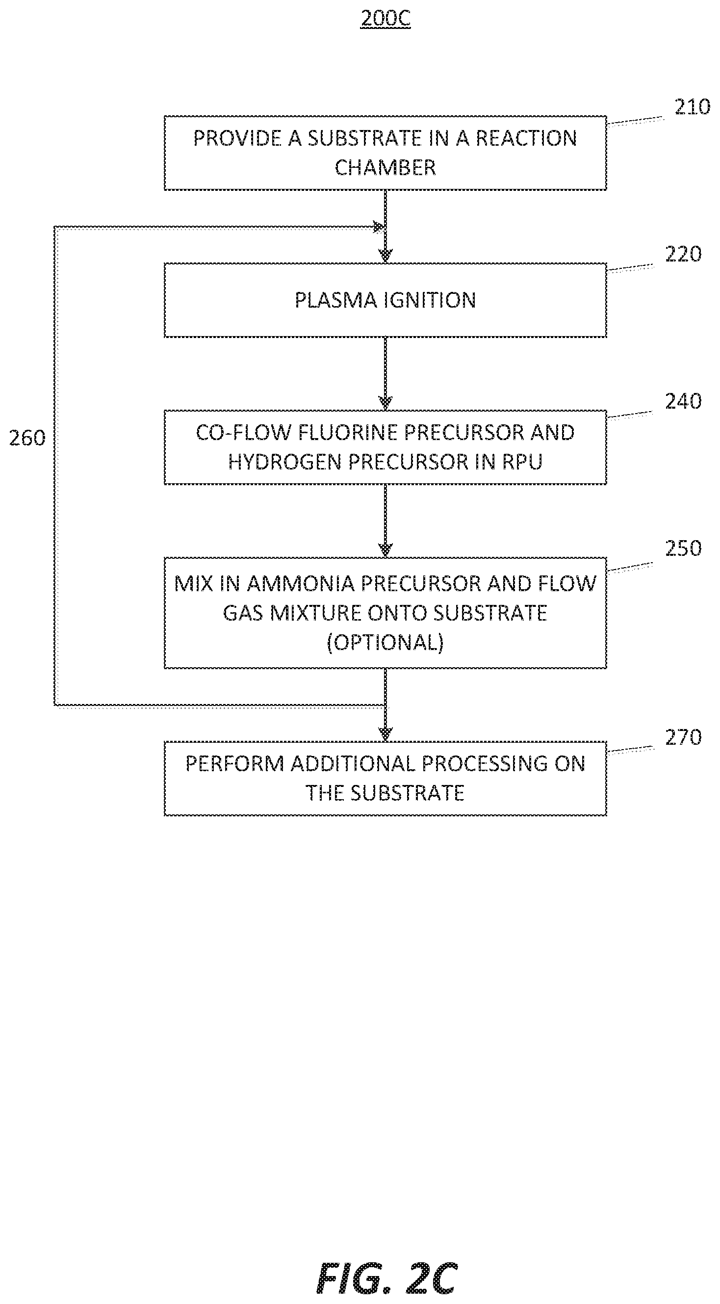
[0031] FIG. 2C illustrates an etching process 200C similar to that shown in FIG. 2A or in FIG. 2B. The main difference is that in the etching process 200C, there is no step for flowing either a hydrogen precursor gas or a fluorine precursor gas in the RPU individually prior to the step of co-flowing a fluorine precursor and a hydrogen precursor in the RPU.
[0032] FIG. 2D illustrates an etching process 200D similar to that shown in FIG. 2A. The etching process 200D may also comprise a step 215 for performing a carbon removal process on the substrate. The carbon removal process may be accomplished by flowing hydrogen (H.sub.2) or ammonia (NH.sub.3) into the RPU with an inert gas to create hydrogen radicals that would remove a carbon layer, a carbon-containing layer, or carbonaceous contaminants from the surface of the substrate.
[0033] An apparatus for performing this step 215 may be an integrated semiconductor processing device that is configured to perform the carbon removal process as well as the etch processes 200A-200C shown in FIGS. 2A-2C. Examples of such an apparatus and methods for removing a carbon layer, a carbon-containing layer, or carbonaceous contaminants are disclosed in U.S. Patent Publication No. 2019/0348261 (entitled "Apparatus for Use with Hydrogen Radicals and Method of Using Same," filed on May 9, 2018), which is hereby incorporated by reference herein.
[0034] As a result of the processes described above, interfacial impurities may be reduced. The interfacial impurities may be caused by floating nitrogen atoms/radicals/ions that may embed into exposed surfaces on the substrate. The reduction of interfacial impurities may be reduced by a percentage ranging between 0 and 100%, between 50 and 100%, or between 90 and 99%.
[0035] At the same time, the processes described above may maintain the non-etched layer to prevent significant loss of the non-etched layer. For example, in a situation where a substrate has both a silicon oxide layer and a silicon nitride layer, the processes described above may allow for more selective etching of the silicon oxide layer compared to etching of the silicon nitride layer. A selectivity of etching the silicon oxide layer to etching the silicon nitride layer may be described in a ratio exceeding 20:1, or a ratio exceeding 100:1, or a ratio exceeding 200:1.
[0036] In accordance with at least one embodiment of the invention, a substrate processing system 300 is disclosed in FIG. 3. The substrate processing system 300 may comprise: a reaction chamber 310; a remote plasma unit 320; a fluorine precursor gas source 330A; a hydrogen precursor gas source 330B; a nitrogen precursor gas source; an inert gas source 330C; an ammonia (or ammonia precursor) source 330D; a pathway 340 disposed between the remote plasma unit 320 and the reaction chamber 310; and a plurality of gas lines 350A-350D linking the gas sources 330A-330D with the remote plasma unit 320. In various embodiments, a substrate processing system may comprise multiple remote plasma units (e.g., one coupled to the fluorine source for producing a fluorine radical, and one coupled to the hydrogen source for producing a hydrogen radical).
[0037] The particular implementations shown and described are illustrative of the invention and its best mode and are not intended to otherwise limit the scope of the aspects and implementations in any way. Indeed, for the sake of brevity, conventional manufacturing, connection, preparation, and other functional aspects of the system may not be described in detail. Furthermore, the connecting lines shown in the various figures are intended to represent exemplary functional relationships and/or physical couplings between the various elements. Many alternative or additional functional relationship or physical connections may be present in the practical system, and/or may be absent in some embodiments.
[0038] It is to be understood that the configurations and/or approaches described herein are exemplary in nature, and that these specific embodiments or examples are not to be considered in a limiting sense, because numerous variations are possible. The specific routines or methods described herein may represent one or more of any number of processing strategies. Thus, the various acts illustrated may be performed in the sequence illustrated, in other sequences, or omitted in some cases.
[0039] The subject matter of the present disclosure includes all novel and nonobvious combinations and subcombinations of the various processes, systems, and configurations, and other features, functions, acts, and/or properties disclosed herein, as well as any and all equivalents thereof.
* * * * *
D00000
D00001
D00002
D00003
D00004
D00005
D00006
XML
uspto.report is an independent third-party trademark research tool that is not affiliated, endorsed, or sponsored by the United States Patent and Trademark Office (USPTO) or any other governmental organization. The information provided by uspto.report is based on publicly available data at the time of writing and is intended for informational purposes only.
While we strive to provide accurate and up-to-date information, we do not guarantee the accuracy, completeness, reliability, or suitability of the information displayed on this site. The use of this site is at your own risk. Any reliance you place on such information is therefore strictly at your own risk.
All official trademark data, including owner information, should be verified by visiting the official USPTO website at www.uspto.gov. This site is not intended to replace professional legal advice and should not be used as a substitute for consulting with a legal professional who is knowledgeable about trademark law.