Methods For Selective Deposition Of Doped Semiconductor Material
Barbosa Lima; Lucas Petersen ; et al.
U.S. patent application number 17/064041 was filed with the patent office on 2021-04-22 for methods for selective deposition of doped semiconductor material. The applicant listed for this patent is ASM IP Holding B.V.. Invention is credited to Lucas Petersen Barbosa Lima, Rami Khazaka, Qi Xie.
| Application Number | 20210118679 17/064041 |
| Document ID | / |
| Family ID | 1000005192305 |
| Filed Date | 2021-04-22 |


| United States Patent Application | 20210118679 |
| Kind Code | A1 |
| Barbosa Lima; Lucas Petersen ; et al. | April 22, 2021 |
METHODS FOR SELECTIVE DEPOSITION OF DOPED SEMICONDUCTOR MATERIAL
Abstract
Methods and systems for selectively depositing material, such as doped semiconductor material, are disclosed. An exemplary method includes providing a substrate, comprising a first area comprising a first material and a second area comprising a second material, selectively depositing a first doped semiconductor layer overlying the first material relative to the second material and selectively depositing a second doped semiconductor layer overlying the first doped semiconductor layer relative to the second material.
| Inventors: | Barbosa Lima; Lucas Petersen; (Heverlee, BE) ; Khazaka; Rami; (Leuven, BE) ; Xie; Qi; (Wilsele, BE) | ||||||||||
| Applicant: |
|
||||||||||
|---|---|---|---|---|---|---|---|---|---|---|---|
| Family ID: | 1000005192305 | ||||||||||
| Appl. No.: | 17/064041 | ||||||||||
| Filed: | October 6, 2020 |
Related U.S. Patent Documents
| Application Number | Filing Date | Patent Number | ||
|---|---|---|---|---|
| 62916662 | Oct 17, 2019 | |||
| Current U.S. Class: | 1/1 |
| Current CPC Class: | H01L 21/02381 20130101; H01L 29/0843 20130101; C23C 16/455 20130101; H01L 21/02488 20130101; H01L 21/02579 20130101; H01L 21/02532 20130101; H01L 21/02384 20130101 |
| International Class: | H01L 21/02 20060101 H01L021/02; H01L 29/08 20060101 H01L029/08; C23C 16/455 20060101 C23C016/455 |
Claims
1. A selective deposition method comprising the steps of: providing a substrate, comprising a surface comprising a first area comprising a first material and a second area comprising a second material, within a reaction chamber; selectively and epitaxially depositing a first doped semiconductor layer overlying the first material; and selectively and epitaxially depositing a second doped semiconductor layer overlying the first doped semiconductor layer; wherein the first material comprises a doped or undoped monocrystalline material selected from the list consisting of silicon (Si), silicon germanium (SiGe), germanium tin (GeSn), silicon germanium tin (SiGeSn), and germanium (Ge); wherein the second material comprises a non-monocrystalline dielectric material selected from silicon oxide, silicon nitride, silicon oxynitride, silicon carbide, silicon oxycarbide, and mixtures thereof.
2. The method of claim 1, wherein the first doped semiconductor layer comprises boron-doped silicon germanium.
3. The method of claim 1, wherein the first doped semiconductor layer comprises a lower part and an upper part, wherein the lower part comprises p-type germanium, and wherein the upper part comprises p-type silicon germanium.
4. The method of claim 3, wherein the p-type germanium comprises boron and gallium doped germanium.
5. The method of claim 4, wherein the p-type silicon germanium comprises boron-doped silicon germanium.
6. The method of claim 1 wherein the second doped semiconductor layer comprises p-type silicon.
7. The method according to claim 6, wherein the p-type silicon comprises boron-doped silicon.
8. The method according to claim 6, wherein the p-type silicon comprises boron and gallium-doped silicon.
9. The method of claim 1, wherein the step of selectively depositing the first doped semiconductor layer comprises simultaneously flowing a precursor and an etchant to the reaction chamber, wherein the etchant comprises hydrogen chloride and/or chlorine.
10. The method of claim 1, wherein selectively depositing the first doped semiconductor layer and/or selectively depositing the second doped semiconductor layer comprises alternating cycles of flowing one or more precursors to the reaction chamber, and of flowing an etchant to the reaction chamber.
11. The method of claim 10, wherein the etchant comprises a halide gas, wherein the halide gas is selected from the group consisting of hydrogen chloride and chlorine.
12. The method of claim 1, wherein the step of selectively depositing the first doped semiconductor layer comprises depositing a p-type doped silicon germanium layer, and wherein the step of selectively depositing the second doped semiconductor layer comprises selectively depositing a gallium-doped layer overlying the p-type doped silicon germanium layer.
13. A transistor device comprising a source region formed using the method of claim 1, wherein the device further includes a drain region formed using a method according to claim 1.
14. The transistor device of claim 13, wherein the source region and/or the drain region comprise a second doped semiconductor layer comprising about 1.times.10.sup.19 charge carriers/cm.sup.3 to about 5.times.10.sup.21 charge carriers/cm.sup.3.
15. The transistor device of claim 13, wherein the source region and/or the drain region comprise a second doped semiconductor layer comprising about 10% to about 90% germanium.
16. The transistor device of claim 13, wherein the source region and/or the drain region comprise a first doped semiconductor layer having a thickness of between about 1 nm and 20 nm, and wherein the source region and/or the drain region comprise a second doped semiconductor layer having a thickness between about 1 nm and 20 nm.
17. A system comprising: one or more reaction chambers; a gas injection system fluidly coupled to at least one of the one or more reaction chambers; a first gas source; a second gas source; a third gas source; an exhaust source; and a controller, wherein the controller is configured to control gas flow into the gas injection system to selectively form a first doped semiconductor layer overlying a first surface of a substrate relative to a second surface of the substrate and selectively form a second doped semiconductor layer overlying the first doped semiconductor layer.
18. The system of claim 17, wherein the controller is configured to perform a step of etching the first doped semiconductor layer overlying the second surface in the one or more reaction chambers.
19. The system of claim 17, wherein the first gas source comprises a silicon precursor source, wherein the second gas source comprises a germanium precursor source, and wherein the third gas source comprises a boron precursor source.
20. The system of claim 19, further comprising a fourth gas source, the fourth gas source comprising a gallium precursor source.
Description
CROSS-REFERENCE TO RELATED APPLICATIONS
[0001] This application claims priority to U.S. Provisional Patent Application Ser. No. 62/916,662 filed Oct. 17, 2019 titled METHODS FOR SELECTIVE DEPOSITION OF DOPED SEMICONDUCTOR MATERIAL, the disclosure of which is hereby incorporated by reference in its entirety.
FIELD OF INVENTION
[0002] The present disclosure generally relates to methods and systems suitable for forming electronic devices. More particularly, the disclosure relates to methods and systems that can be used for selectively depositing material, such as doped semiconductor material, on a surface of a substrate.
BACKGROUND OF THE DISCLOSURE
[0003] The scaling of semiconductor devices, such as, for example, complementary metal-oxide-semiconductor (CMOS) devices, has led to significant improvements in speed and density of integrated circuits. However, conventional device scaling techniques face significant challenges for future technology nodes.
[0004] One approach to improve semiconductor device performance is to enhance the carrier mobility, and consequently the transistor drive current, utilizing strain induced effects. For example, it has been shown that the hole mobility may be considerably enhanced in p-channel Group IV semiconductor transistors employing stressor regions, such as, stressor regions employed in the source and drain regions of the transistors.
[0005] Further, reduction in contact resistance to the active regions of a semiconductor device structure may be desirable for on-going device improvement at future technology nodes. For example, for CMOS device structures, a contact resistance may include the electrical resistance between a contact structure and one or more active (e.g., stressor) regions, such as source and drain regions of the transistor structure. In the case of an n-type MOS device, the stressor region may comprise a highly doped region, i.e., with a carrier density of approximately 5.times.10.sup.20 cm.sup.-3 or more, doped with either phosphorus or arsenic. The high doping levels that may be achieved in the n-type MOS device stressor region may result in a contact resistivity below 0.3 m.OMEGA.-cm. However, for the p-type MOS device, the current state of the art has focused on the use of p-type doping utilizing boron as a dopant. In some cases, boron may have relatively low solubility in the semiconductor material, and thus high concentrations of the p-type dopant and thus low contact resistance to the semiconductor material can be difficult to obtain.
[0006] By way of examples, attempts to lower the contact resistance of silicon germanium films include growing SiGe layers with high boron concentrations. However, high boron concentrations are difficult to achieve with higher Ge:Si ratios due to the low boron solubility in germanium, and therefore, attempts to simply increase the boron concentration in the silicon germanium film have generally not been sufficient to decrease the contact resistivity of the silicon germanium layers to desired values.
[0007] Further attempts to decrease the contact resistance to the silicon germanium and similar films include the addition of another dopant, in which the first dopant (e.g., boron) may be soluble, and a high-temperature anneal process. Such techniques may be problematic because the use of the relatively high temperatures during the anneal process can lead to clustering of one or more of the dopants of the doped semiconductor films.
[0008] Furthermore, in many applications, it may be desirable to selectively deposit semiconductor material (e.g., highly-doped Group IV semiconductor material) with a first dopant (e.g., boron) and a second dopant (e.g., gallium, aluminum or indium). However, such techniques may not be well developed. Accordingly, improved methods and systems for depositing doped semiconductor material are desired.
[0009] Any discussion, including discussion of problems and solutions, set forth in this section has been included in this disclosure solely for the purpose of providing a context for the present disclosure. Such discussion should not be taken as an admission that any or all of the information was known at the time the invention was made or otherwise constitutes prior art.
SUMMARY OF THE DISCLOSURE
[0010] Various embodiments of the present disclosure relate to selective deposition methods, to structures and devices formed using such methods, and to apparatus for performing the methods and/or for forming the structure and/or devices. While the ways in which various embodiments of the present disclosure address drawbacks of prior methods and systems are discussed in more detail below, in general, various embodiments of the disclosure provide improved methods of selectively depositing doped semiconductor layers. The doped semiconductor layers can exhibit relatively low contact resistance. Additionally or alternatively, the doped semiconductor layers can be formed at relatively low temperatures--e.g., 350.degree. C. to 600.degree. C. or less, without the use of a step of annealing to improve the contact resistance of the doped semiconductor layers.
[0011] In accordance with exemplary embodiments of the disclosure, a selective deposition method is disclosed. Exemplary selective deposition methods include providing a substrate, comprising a surface comprising a first area comprising a first material and a second area comprising a second material, within a reaction chamber; selectively depositing a first doped semiconductor layer overlying the first material; and selectively depositing a second doped semiconductor layer overlying the first doped semiconductor layer. The first material can include, for example, semiconductor material, such as silicon, silicon germanium, germanium tin, silicon germanium tin, germanium, or the like. The second material can include, for example, a dielectric material, such as an oxide, a nitride, an oxynitride, an oxycarbide, an oxycarbide nitride, and/or the like, such as silicon nitride, silicon oxide (SiO.sub.2), silicon carbide and mixtures thereof, such as SiOC, SiOCN, SiON. The first doped semiconductor layer can include, for example, p-type or n-type doped Group IV semiconductor material. The second doped semiconductor layer can include, for example, p-type or n-type doped Group IV semiconductor material. The first and second doped semiconductor layers can include the same type (n-type or p-type) doping. In some cases, the first and second doped semiconductor layers can include the same dopant and one of the first and second doped semiconductor layers can include an additional dopant. In some cases, an etchant can be flowed during the step of selectively depositing the first doped semiconductor layer. Additionally or alternatively, exemplary methods can include a step of etching the first doped semiconductor layer material--e.g., to remove first doped semiconductor layer material over the second area. The etching can be performed using a halide-containing gas, such as hydrogen chloride, chlorine or the like. In accordance with some examples of the disclosure, the step of selectively depositing the first or second doped semiconductor layer does not include exposing the surface to a gas comprising an etchant and/or a gas comprising a halide. As set forth in more detail below, various steps of exemplary methods described herein can be performed in the same reaction chamber or in different reaction chambers of, for example, the same cluster tool.
[0012] In accordance with further exemplary embodiments of the disclosure, a structure is formed using a method as described herein. The structure can include a substrate having a surface including a first area comprising a first material and a second area comprising a second material, a first doped semiconductor layer overlying the first material, and a second doped semiconductor layer overlying the first doped semiconductor layer. The first doped semiconductor layer material and the second doped semiconductor layer material can be the same or similar to the respective materials described above and elsewhere herein.
[0013] In accordance with yet additional embodiments of the disclosure, a device or portion thereof can be formed using a method and/or a structure as described herein. The device can include a substrate, a first doped semiconductor layer, a second doped semiconductor layer, and a conducting layer overlying the second doped semiconductor layer. The first doped semiconductor layer and/or the second doped semiconductor layer can be used to form a source or drain region of the device, such as a field effect transistor (FET) (e.g., a FinFET).
[0014] In accordance with yet additional examples of the disclosure, a system to perform a method as described herein and/or to form a structure, device, or portion of either is disclosed.
[0015] Further described herein is a selective deposition method comprising the steps of: providing a substrate, comprising a surface comprising a first area comprising a first material and a second area comprising a second material, within a reaction chamber; selectively and epitaxially depositing a first doped semiconductor layer overlying the first material; and selectively and epitaxially depositing a second doped semiconductor layer overlying the first doped semiconductor layer; wherein the first material comprises a doped or undoped monocrystalline material selected from the list consisting of silicon (Si), silicon germanium (SiGe), germanium tin (GeSn), silicon germanium tin (SiGeSn), and germanium (Ge); and, wherein the second material comprises a non-monocrystalline dielectric material selected from silicon oxide, silicon nitride, silicon oxynitride, silicon carbide, silicon oxycarbide, and mixtures thereof.
[0016] In some embodiments, the first doped semiconductor layer comprises boron-doped silicon germanium.
[0017] In some embodiments, the first doped semiconductor layer comprises a lower part and an upper part, wherein the lower part comprises p-type germanium, and wherein the upper part comprises p-type silicon germanium.
[0018] In some embodiments, the p-type germanium comprises boron and gallium doped germanium.
[0019] In some embodiments, the p-type silicon germanium comprises boron-doped silicon germanium.
[0020] In some embodiments, the second doped semiconductor layer comprises p-type silicon.
[0021] In some embodiments, the p-type silicon comprises boron-doped silicon.
[0022] In some embodiments, the p-type silicon comprises boron and gallium-doped silicon.
[0023] In some embodiments, the step of selectively depositing the first doped semiconductor layer comprises simultaneously flowing a precursor and an etchant to the reaction chamber, wherein the etchant comprises hydrogen chloride and/or chlorine.
[0024] In some embodiments, selectively depositing the first doped semiconductor layer and/or selectively depositing the second doped semiconductor layer comprises alternating cycles of flowing one or more precursors to the reaction chamber, and of flowing an etchant to the reaction chamber.
[0025] In some embodiments, the etchant comprises a halide gas, wherein the halide gas is selected from the group consisting of hydrogen chloride and chlorine.
[0026] In some embodiments, the step of selectively depositing the first doped semiconductor layer comprises depositing a p-type doped silicon germanium layer, and the step of selectively depositing the second doped semiconductor layer comprises selectively depositing a gallium-doped layer overlying the p-type doped silicon germanium layer.
[0027] Further described is a transistor device comprising a source region formed using a method as described; wherein the device further includes a drain region formed using a method as described herein.
[0028] In some embodiments, the source region and/or the drain region comprise a second doped semiconductor layer comprising about 1.times.10.sup.19 charge carriers/cm.sup.3 to about 1.times.10.sup.21 charge carriers/cm.sup.3, or about 1.times.10.sup.19 charge carriers/cm.sup.3 to about 5.times.10.sup.21 charge carriers/cm.sup.3.
[0029] In some embodiments, the source region and/or the drain region comprise a second doped semiconductor layer comprising about 10% to about 90%, or about 35% to about 70%, or about 40% to about 50% silicon; and the second doped semiconductor layer comprises about 10% to about 90%, or about 65% to about 30%, or about 60% to about 50% germanium.
[0030] In some embodiments, the source region and/or the drain region comprise a first doped semiconductor layer having a thickness of between about 1 nm and 20 nm; and the source region and/or the drain region comprise a second doped semiconductor layer having a thickness between about 1 nm and 20 nm.
[0031] Further described is a system comprising: one or more reaction chambers; a gas injection system fluidly coupled to at least one of the one or more reaction chambers; a first gas source; a second gas source; a third gas source; an exhaust source; and a controller, wherein the controller is configured to control gas flow into the gas injection system to selectively form a first doped semiconductor layer overlying a first surface of a substrate relative to a second surface of the substrate and selectively form a second doped semiconductor layer overlying the first doped semiconductor layer.
[0032] In some embodiments, the controller is configured to perform a step of etching the first doped semiconductor layer overlying the second surface in the one or more reaction chambers.
[0033] In some embodiments, the first gas source comprises a silicon precursor source, wherein the second gas source comprises a germanium precursor source, and wherein the third gas source comprises a boron precursor source.
[0034] In some embodiments, the system further comprises a fourth gas source, the fourth gas source comprising a gallium precursor source.
[0035] These and other embodiments will become readily apparent to those skilled in the art from the following detailed description of certain embodiments having reference to the attached figures. The invention is not being limited to any particular embodiments disclosed.
BRIEF DESCRIPTION OF THE DRAWING FIGURES
[0036] A more complete understanding of the embodiments of the present disclosure may be derived by referring to the detailed description and claims when considered in connection with the following illustrative figures.
[0037] FIG. 1 illustrates a method in accordance with exemplary embodiments of the disclosure.
[0038] FIG. 2 illustrates a substrate for use in accordance with examples of the disclosure.
[0039] FIGS. 3-5 illustrate structures in accordance with exemplary embodiments of the disclosure.
[0040] FIG. 6 illustrates a portion of a device in accordance with exemplary embodiments of the disclosure.
[0041] FIG. 7 illustrates a reactor system in accordance with additional exemplary embodiments of the disclosure.
[0042] FIG. 8 illustrates a method in accordance with exemplary embodiments of the disclosure.
[0043] It will be appreciated that elements in the figures are illustrated for simplicity and clarity and have not necessarily been drawn to scale. For example, the dimensions of some of the elements in the figures may be exaggerated relative to other elements to help improve understanding of illustrated embodiments of the present disclosure.
DETAILED DESCRIPTION OF EXEMPLARY EMBODIMENTS
[0044] The description of exemplary embodiments of methods, structures, devices and systems provided below is merely exemplary and is intended for purposes of illustration only; the following description is not intended to limit the scope of the disclosure or the claims. Moreover, recitation of multiple embodiments having stated features is not intended to exclude other embodiments having additional features or other embodiments incorporating different combinations of the stated features. For example, various embodiments are set forth as exemplary embodiments and may be recited in the dependent claims. Unless otherwise noted, the exemplary embodiments or components thereof may be combined or may be applied separate from each other.
[0045] As set forth in more detail below, various embodiments of the disclosure provide methods for selectively depositing doped semiconductor material on a surface of a substrate. Exemplary methods can be used to, for example, form source and/or drain regions of semiconductor devices that exhibit relatively high mobility, relatively low contact resistance, and that maintain the structure and composition of the deposited layers. For example, methods described herein can include selectively depositing a first doped semiconductor layer overlying a first material relative to a second material and selectively depositing a second doped semiconductor layer overlying the first doped semiconductor layer--e.g., relative to the second material. The first doped semiconductor layer may be suitable for selective deposition, but may not exhibit desired properties--such as low contact resistance. The second doped semiconductor layer may be less suitable for selective deposition (over the first material relative to the second material), but may exhibit the desired properties and may be selective with respect to the first doped semiconductor layer relative to the second material. Accordingly, use of the first doped semiconductor layer and the second doped semiconductor layer can result in selective deposition of films with desired properties.
[0046] In this disclosure, "gas" can include material that is a gas at normal temperature and pressure (NTP), a vaporized solid and/or a vaporized liquid, and can be constituted by a single gas or a mixture of gases, depending on the context. A gas other than the process gas, i.e., a gas introduced without passing through a gas distribution assembly, a multi-port injection system, other gas distribution device, or the like, can be used for, e.g., sealing the reaction space, and can include a seal gas, such as a rare gas. In some cases, the term "precursor" can refer to a compound that participates in the chemical reaction that produces another compound, and particularly to a compound that constitutes a film matrix or a main skeleton of a film; the term "reactant" can be used interchangeably with the term precursor. The term "inert gas" can refer to a gas that does not take part in a chemical reaction and/or does not become a part of a film matrix to an appreciable extent. Exemplary inert gases include He, Ar, N.sub.2, and any combination thereof.
[0047] As used herein, the term "substrate" can refer to any underlying material or materials that can be used to form, or upon which, a device, a circuit, or a film can be formed. A substrate can include a bulk material, such as silicon (e.g., single-crystal silicon), other Group IV materials, such as germanium, or other semiconductor materials, such as a Group II-VI or Group III-V semiconductor, and can include one or more layers overlying or underlying the bulk material. Further, the substrate can include various features, such as recesses, protrusions, and the like formed within or on at least a portion of a layer of the substrate. As set forth in more detail below, a surface of a substrate can include two or more areas, wherein each of the two or more areas comprise different material and/or the same material with different crystalline structure.
[0048] As used herein, the term "epitaxial layer" can refer to a substantially single crystalline layer upon an underlying substantially single crystalline substrate or layer.
[0049] As used herein, the term "chemical vapor deposition" can refer to any process wherein a substrate is exposed to one or more volatile precursors, which react and/or decompose on a substrate surface to produce a desired deposition.
[0050] As used herein, the term "silicon germanium" can refer to a semiconductor material comprising silicon and/or germanium and can be represented as Si.sub.1-xGe.sub.x wherein 1.gtoreq.x .gtoreq.0, or 0.2.gtoreq.x.gtoreq.0.8, or 0.4.gtoreq.x.gtoreq.0.6.
[0051] As used herein, the term "film" and/or "layer" can refer to any continuous or non-continuous structures and material, such as material deposited by the methods disclosed herein. For example, film and/or layer can include two-dimensional materials, three-dimensional materials, nanoparticles or even partial or full molecular layers or partial or full atomic layers or clusters of atoms and/or molecules. A film or layer may comprise material or a layer with pinholes, which may be at least partially continuous.
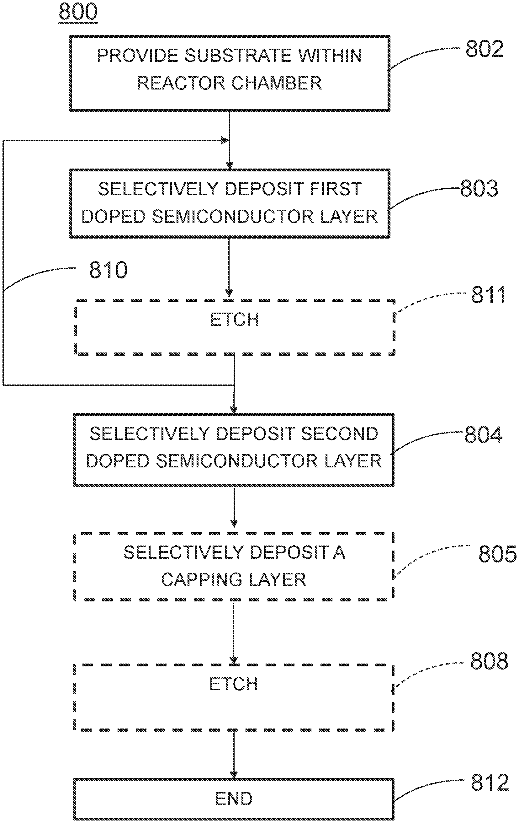
[0052] As used herein, a "structure" can include a substrate as described herein. Structures can include one or more layers overlying the substrate, such as one or more layers formed according to a method as described herein.
[0053] As used herein, the term "Group IV semiconductor" may refer to a semiconductor material comprising at least one of carbon (C), silicon (Si), germanium (Ge), tin (Sn), or alloys thereof.
[0054] As used herein, the term "Group IIIA dopant precursor" may refer to dopant precursor comprising at least one of boron (B), aluminum (Al), gallium (Ga), or indium (In). Similarly, a p-type dopant can include one or more of B, Al, Ga, and In.
[0055] As used herein, the term "Group V dopant precursor" may refer to dopant precursor comprising at least one of phosphorus (P), arsenic (As), and antimony (Sb). Similarly, an n-type dopant can include one or more of P, As, and Sb.
[0056] Further, in this disclosure, any two numbers of a variable can constitute a workable range of the variable, and any ranges indicated may include or exclude the endpoints. Additionally, any values of variables indicated (regardless of whether they are indicated with "about" or not) may refer to precise values or approximate values and include equivalents, and may refer to average, median, representative, majority, or the like. Further, in this disclosure, the terms "including," "constituted by" and "having" refer independently to "typically or broadly comprising," "comprising," "consisting essentially of," or "consisting of" in some embodiments. In this disclosure, any defined meanings do not necessarily exclude ordinary and customary meanings in some embodiments.
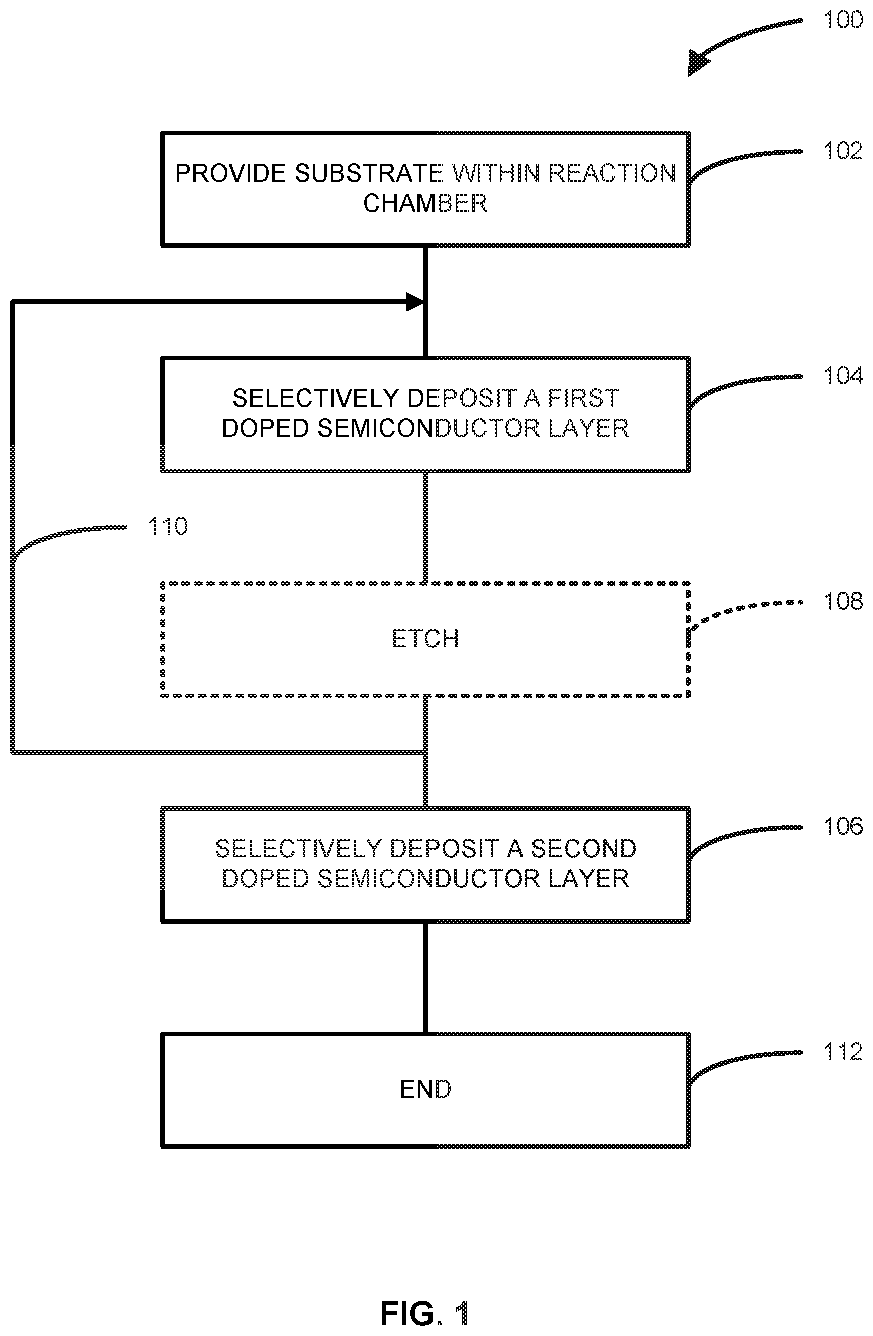
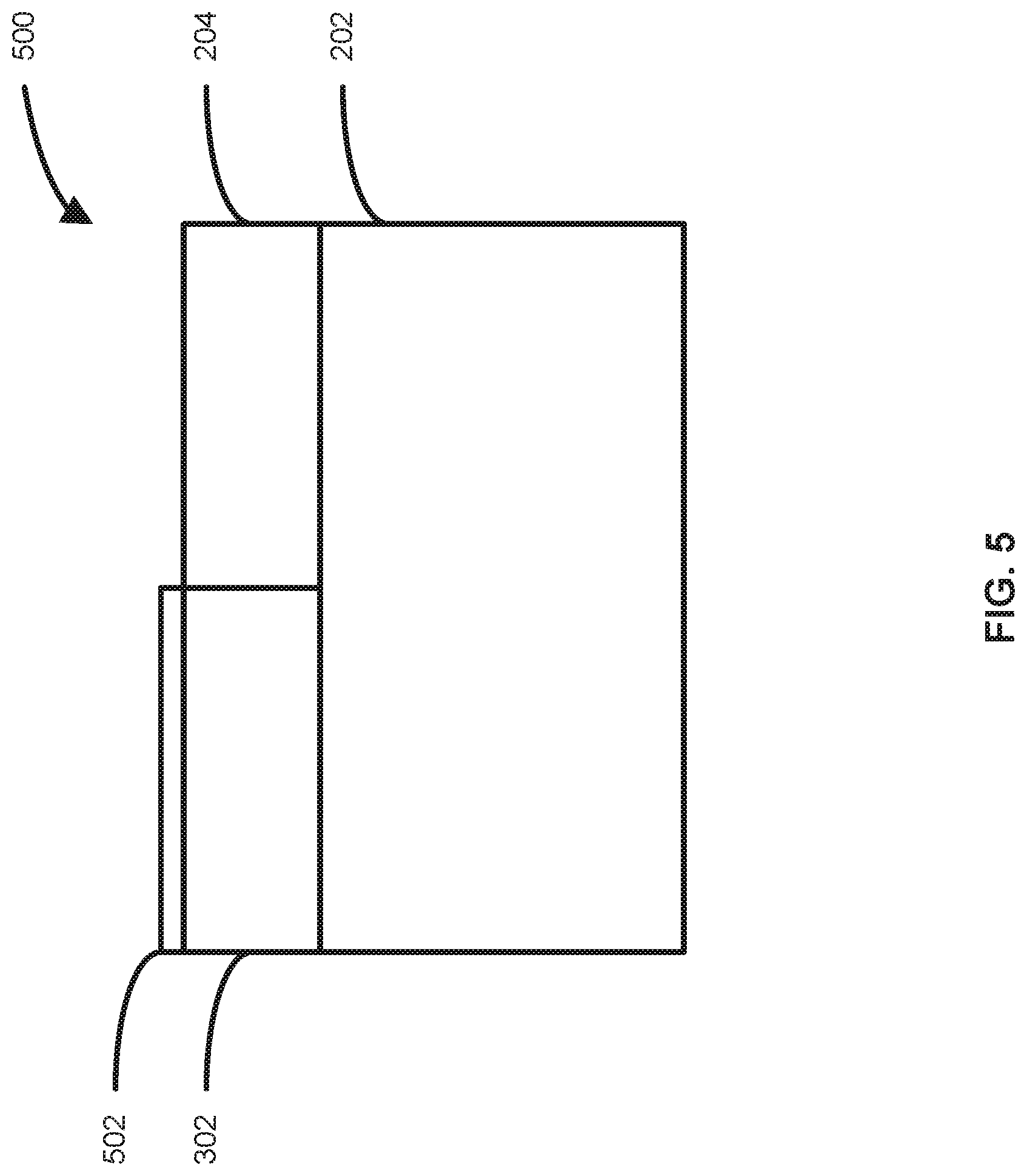
[0057] Turning now to the figures, FIG. 1 illustrates a (e.g., selective deposition) method 100 in accordance with exemplary embodiments of the disclosure. FIGS. 2-5 illustrate structures 200, 300, 400, and 500 that can correspond to steps of method 100.
[0058] Method 100 includes the steps of providing a substrate within a reaction chamber (step 102), selectively depositing a first doped semiconductor layer (step 104), selectively depositing a second doped semiconductor layer (step 106), an optional etching step (step 108), optionally repeating steps 104 and 108 (loop 110), optionally repeating step 106, and ending (step 112).
[0059] With reference to FIG. 1 and FIG. 2, a substrate (or structure) 200 provided during step 102 can include a first area 206 comprising a first material (e.g., (mono)crystalline bulk material 202) and a second area 208 comprising a second material (e.g., non-monocrystalline material 204). The first material can include a monocrystalline surface 210; second area 208 can include a non-monocrystalline surface 212, such as a polycrystalline surface or an amorphous surface. Monocrystalline surface 210 may include, for example, one or more of: silicon (Si), silicon germanium (SiGe), germanium tin (GeSn), silicon germanium tin (SiGeSn), or germanium (Ge). The first material may be doped with a dopant. Exemplary dopants include boron, gallium, phosphorous, and arsenic. Non-monocrystalline surface 212 may include, for example, dielectric materials, such as oxides, oxynitrides, nitrides, oxycarbides, or oxycarbide nitrides, including, for example, silicon oxides, silicon nitrides, silicon oxynitrides, silicon carbides and mixtures thereof, such as SiOC, SiOCN, SiON.
[0060] As a non-limiting example, the reaction chamber used during step 102 may comprise a reaction chamber of a chemical vapor deposition system. However, it is also contemplated that other reaction chambers and alternative chemical vapor deposition systems may also be utilized to perform the embodiments of the present disclosure. The reaction chamber can be a stand-alone reaction chamber or part of a cluster tool.
[0061] Step 102 can include heating the substrate to a desired deposition temperature within the reaction chamber. In some embodiments of the disclosure, step 102 includes heating the substrate to a temperature of less than approximately 1100.degree. C., or to a temperature of less than approximately 700.degree. C., or to a temperature of less than approximately 650.degree. C., or to a temperature of less than approximately 600.degree. C., or to a temperature of less than approximately 550.degree. C., or to a temperature of less than approximately 500.degree. C., or to a temperature of less than approximately 450.degree. C., or even to a temperature of less than approximately 400.degree. C., such as a temperature of at least 350.degree. C. to at most 400.degree. C. For example, in some embodiments of the disclosure, heating the substrate to a deposition temperature may comprise heating the substrate to a temperature between approximately 400.degree. C. and approximately 700.degree. C.
[0062] In addition to controlling the temperature of the substrate, a pressure within the reaction chamber may also be regulated. For example, in some embodiments of the disclosure, the pressure within the reaction chamber during step 102 may be less than 760 Torr, or less than 350 Torr, or less than 100 Torr, or less than 50 Torr, or less than 25 Torr, or even less than 10 Torr. In some embodiments, the pressure in the reaction chamber may be between 10 Torr and 200 Torr.
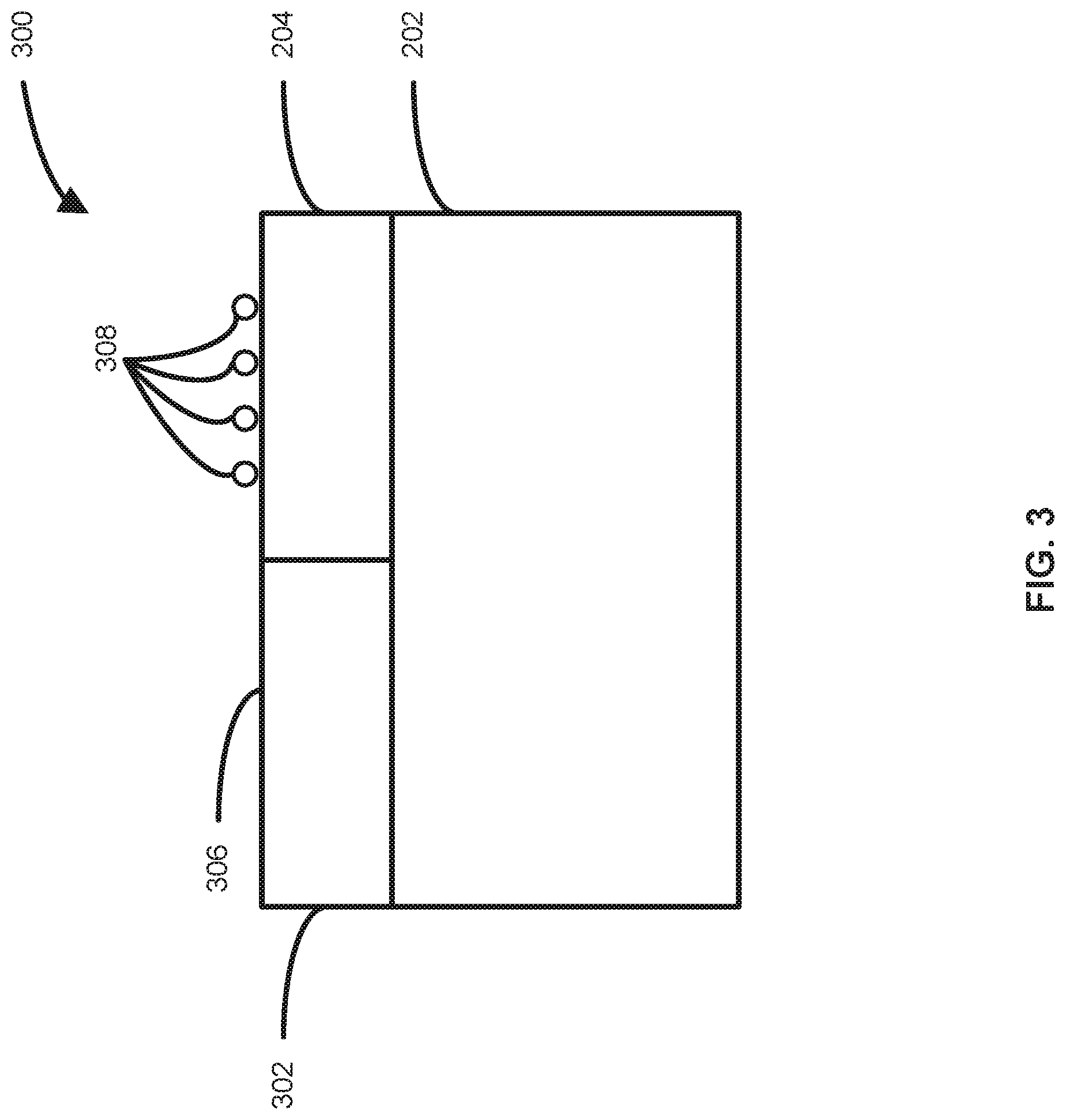
[0063] During step 104, a first doped semiconductor layer 302 is selectively deposited overlying the first material (e.g., bulk material 202) in first area 206 relative to the second material (e.g., non-monocrystalline material 204) in second area 208, as illustrated in FIG. 3. First doped semiconductor layer 302 may form as a (e.g., mono) crystalline material overlying the first area/surface (e.g., area 206/surface 210). Surface 306 of first doped semiconductor layer 302 may therefore be monocrystalline and serve as a template for further epitaxial layers.
[0064] As further illustrated in FIG. 3, structure 300, including a first doped semiconductor layer 302 selectively formed in first area 206, can include some--e.g., nuclei and/or clusters--components 308 of first doped semiconductor material that form in second area 208. In such cases, an etch process, described in more detail below, can be used to remove components 308. In other cases, a nucleation delay of the first doped semiconductor layer may be high enough on the second/non-monocrystalline surface 212 relative to the first surface 210, such that components 308 do not form. In addition, in other cases, the first doped semiconductor layer is grown via selective epitaxial process and, therefore, no layer is formed on the non-monocrystalline surface 212. In such cases, an etch step may not be desired.
[0065] First doped semiconductor layer 302 can include a Group IV semiconductor material. Exemplary Group IV semiconductors include silicon (e.g., n-type doped Si), silicon germanium (SiGe) (e.g., p-type doped SiGe), germanium (e.g., p-type doped Ge), and germanium tin (e.g., p-type doped GeSn). Exemplary dopants include, for example, Group IIIA metals as a p-type dopant and Group V dopants as an n-type dopant.
[0066] During step 104, one or more Group IV precursors and one or more Group IIIA and/or Group V dopant precursors are flowed into the reaction chamber--e.g., through one or more gas injectors, such as multi-port injectors (MPIs) including a plurality of individual port injectors for providing a gas mixture into the reaction chamber. Various combinations of the precursors can be supplied to one or more of the individual port injectors to fine tune concentration profiles as desired. To mitigate reaction with some dopants, such as gallium in the films as the films deposit, the precursors (e.g., all the precursors) may desirably be halide (e.g., chlorine) free. In other words, a chemical formula of a precursor, or component thereof, may not include Cl or other halide.
[0067] In some embodiments, a single Group IV precursor may be utilized during the deposition process; for example, a single Group IV precursor may be utilized when the Group IV semiconductor to be deposited comprises silicon (Si) or germanium (Ge). In some embodiments, two or more Group IV precursors may be utilized during the deposition process; for example, two or more Group IV precursors may be utilized when the Group IV semiconductor to be deposited comprises a Group IV semiconductor alloy including, but not limited to, silicon germanium, silicon germanium carbide (Si.sub.1-x-yGe.sub.xC.sub.y), germanium tin (Ge.sub.1-xSn.sub.x), germanium silicon tin (Ge.sub.1-x-ySi.sub.xSn.sub.y), germanium silicon tin carbide (Ge.sub.1-x-ySi.sub.xSn.sub.yC.sub.x), silicon tin (Si.sub.1-xSn.sub.x), silicon tin carbide (Si.sub.1-x-ySn.sub.xC.sub.y), or silicon carbide (Si.sub.1-xC.sub.x).
[0068] Exemplary silicon precursors (e.g., for deposition of silicon-containing first doped semiconductor layer) may comprise one or more hydrogenated silicon precursors selected from the group comprising: silane (SiH.sub.4), disilane (Si.sub.2H.sub.6), trisilane (Si.sub.3H.sub.8), tetrasilane (Si.sub.4H.sub.10), pentasilane (Si.sub.5H.sub.12), methylsilane (CH.sub.3-SiH.sub.3), and Si.sub.2ClH.sub.2.
[0069] Exemplary germanium precursors (e.g., for deposition of germanium-containing first doped semiconductor layer) may comprise at least one of germane (GeH.sub.4), digermane (Ge.sub.2H.sub.6), trigermane (Ge.sub.3H.sub.8), or germylsilane (GeH.sub.6Si).
[0070] Exemplary tin precursors (e.g., for deposition of tin-containing first doped semiconductor layer) may comprise one tin tetrachloride (SnCl.sub.4).
[0071] A p-type (e.g., boron) dopant precursor can include, for example, at least one of diborane (B.sub.2H.sub.6) or deuterium-diborane (B.sub.2D.sub.6), or one or more borohydrides. Exemplary borohydrides include gallium borohydride (Ga(BH.sub.4).sub.3), aluminum borohydride (Al(BH.sub.4).sub.3), and indium borohydride (In(BH.sub.4).sub.3). In alternative embodiments of the disclosure, the p-type dopant precursor may comprise a borohydride having the formula Y.sub.xM(BH.sub.4).sub.3-x, wherein Y is independently chosen from hydrogen, deuterium, chlorine, bromine, and iodine; M is a Group IIIA metal independently chosen from gallium, aluminum, and indium; and x is an integer from 0-2.
[0072] In some embodiments of the disclosure, the p-type dopant precursor includes one or more organic borohydrides having the general formula R.sub.xM(BH.sub.4).sub.3-x, wherein R is independently chosen from CH.sub.3, C.sub.2H.sub.5, C.sub.6H.sub.5, CF.sub.3SO.sub.3, and NH.sub.2; M is a Group IIIA metal independently chosen from gallium, aluminum and indium; and x is an integer from 1-3.
[0073] In some embodiments of the disclosure, the p-type dopant precursor can include one or more halides having the general formula Z.sub.xMY.sub.3-x, wherein Z is independently chosen from hydrogen, deuterium, chlorine, bromine, and iodine; M is a Group IIIA metal independently chosen from gallium, aluminum, and indium; Y is a halide independently chosen from chlorine, bromine, and iodine; and x is an integer from 0-3. In some embodiments of the disclosure, the halide dopant may comprise a dimer structure and therefore methods may comprise selecting the halide to comprise a halide having the formula (Z.sub.xMY.sub.3-x).sub.2, wherein Z is independently chosen from hydrogen, deuterium, chlorine, bromine, and iodine; M is a Group IIIA metal independently chosen from gallium, aluminum, and indium; Y is a halide independently chosen from chlorine, bromine, and iodine; and x is an integer from 0-3.
[0074] In some embodiments of the disclosure, the p-type dopant precursor can include one or more organohalides and may further comprise selecting the one or more organohalides to comprise an organohalide having the general formula R.sub.xMY.sub.3-x, wherein R is independently chosen from CH.sub.3, C.sub.2H.sub.5, C.sub.6H.sub.5, CF.sub.3SO.sub.3, and NH.sub.2; M is a group IIIA metal independently chosen from gallium, aluminum, and indium; Y is a halide independently chosen from chlorine, bromine, and iodine; and x is an integer from 0-3.
[0075] The selection of Group IIIA dopant precursors comprising an organic component may be further beneficial in the deposition of Group IV semiconductors. For example, carbon incorporation into a Group IV semiconductor may further increase the strain in the Group IV semiconductor being deposited. Therefore, in some embodiments of the disclosure, exposing the substrate to at least one Group IIIA precursor further comprises exposing the substrate to at least one of an organic borohydride or an organohalide. In further embodiments, exposing the substrate to at least one of an organic borohydride or an organohalide further comprises incorporating carbon into the first doped semiconductor layer, the atomic percentage (at-%) of carbon in the first doped semiconductor layer being greater than approximately 0.5 at %.
[0076] An exemplary group IIIA dopant precursor includes gallium precursors such as a gallium alkyl. Exemplary gallium alkyls include trimethylgallium and triethylgallium.
[0077] In some embodiments, the p-type dopant precursor may be provided in diluted form and the diluted form may comprise approximately 0.1% to approximately 100% dopant precursor in a carrier gas (if present).
[0078] An n-type dopant precursor can include, for example, at least one of phosphine, and arsine. In some embodiments, the n-type dopant precursor may be provided in diluted form and the diluted form may comprise approximately 1% to approximately 5% dopant precursor in a carrier gas.
[0079] A thickness of the first doped semiconductor layer 302 formed during step 104 in first area 206 can be between greater than zero or about 1 nm and about 50 nm, between about 5 nm and about 30 nm, or between about 7 nm and about 20 nm. A concentration of p-type dopant (e.g., boron) in the p-type doped silicon germanium layer in first area 206 and/or area 208 can range from about 1.times.10.sup.17 at/cm.sup.3 to about 5.times.10.sup.21 at/cm.sup.3, or from about 1.times.10.sup.17 at/cm.sup.3 to about 3.times.10.sup.21 at/cm.sup.3, or from about 1.times.10.sup.18 at/cm.sup.3 to about 2.times.10.sup.21 at/cm.sup.3, or from about 8.times.10.sup.18 at/cm.sup.3 to about 1.times.10.sup.21 at/cm.sup.3 or greater than 1.times.10.sup.19 at/cm.sup.3 dopant or greater than 1.times.10.sup.20 carriers per cubic centimeter, or greater than 2.5.times.10.sup.20 carriers per cubic centimeter, or greater than 5.times.10.sup.20 carriers per cubic centimeter. For SiGe layers, the p-type doped silicon germanium layer in first area 206 and/or area 208 can include about 10% to about 90%, or about 30% to about 70%, or about 40% to about 50% silicon and/or about 10% to about 90%, or about 65% to about 30%, or about 60% to about 50% germanium. In some embodiments, the germanium (and/or other component) content within first doped semiconductor layer 302 may not be constant, but rather may be varied, such that the germanium content (and/or other component) may have a graded composition within the first doped semiconductor layer.
[0080] To facilitate selective deposition, in some cases, an etchant, such as a halogen-containing gas or halide gas--e.g., at least one of chlorine (Cl.sub.2) or hydrogen chloride (HCl) can be provided to the reaction chamber during the step of selectively depositing a first doped semiconductor layer. In other cases, an etchant is not used during step 104.
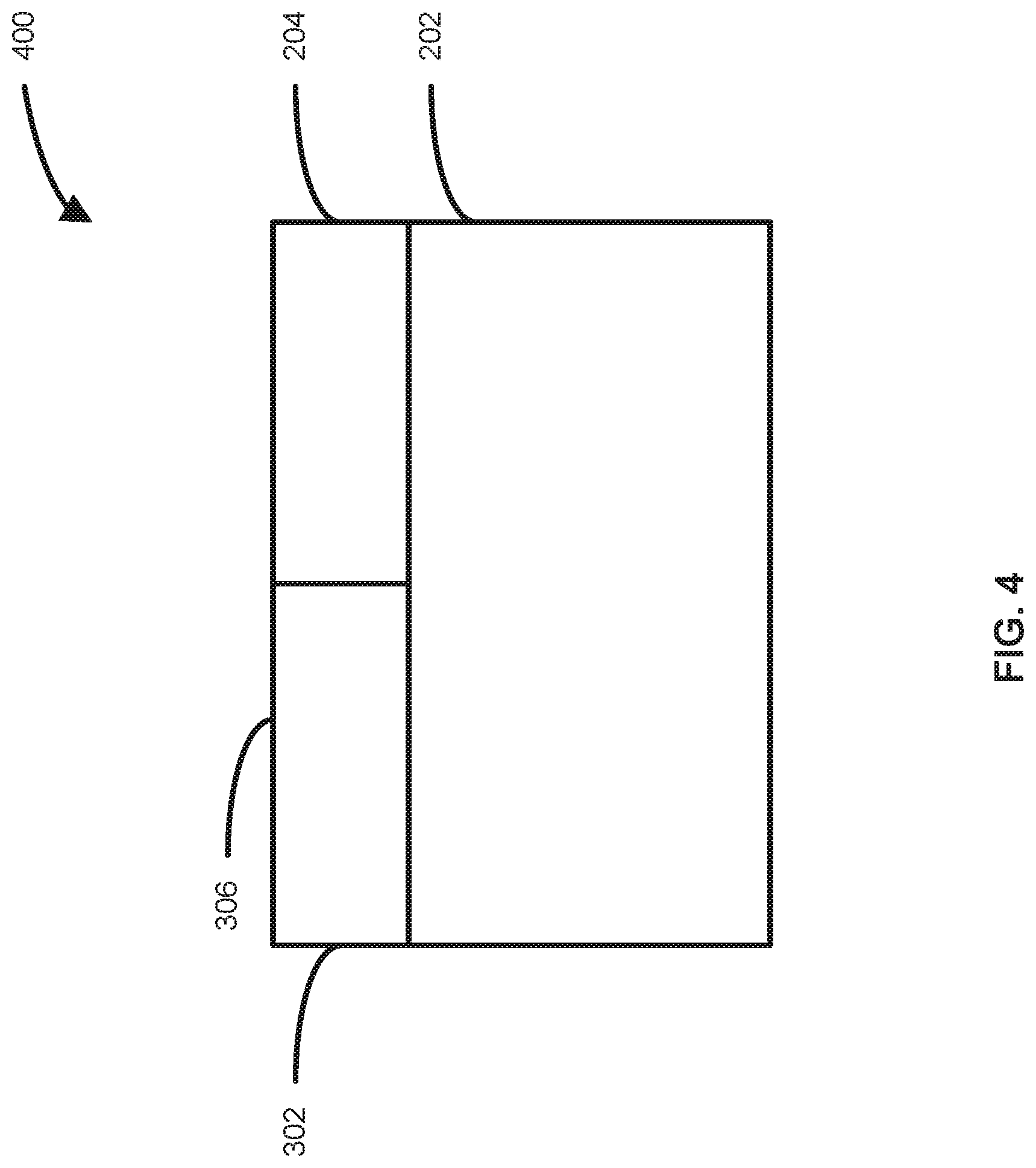
[0081] The method 100 may continue to optional etch step 108. Step 108 can be used to remove any or a portion of the first doped semiconductor layer--e.g., components 308--deposited in second area 208. For example, both (e.g., monocrystalline semiconductor) material in first area 206 and (e.g., non-monocrystalline) material in second area 208 may be exposed to an etchant gas. The etchant may remove (e.g., non-monocrystalline) components 308 in second area 208 at a higher rather than (e.g., monocrystalline semiconductor) material in first area 206 to form structure 400. Step 108 can also be used to refresh the second material for the subsequent processing (e.g., step 106)--e.g., to provide a suitable nucleation delay of the second doped semiconductor layer overlying the second material/area relative to the first material/area. The etchant gas may comprise, for example, a halogen-containing gas or halide gas--e.g., at least one of chlorine (Cl.sub.2) or hydrogen chloride (HCl).
[0082] Step 108 can be performed in the same reaction chamber used during step 104. Alternatively, step 108 can be performed in another reaction chamber, such as another reaction chamber in the same cluster tool as the reaction chamber used during step 104. A temperature and/or pressure for step 108 can be the same or similar to the temperature and/or pressure described above in connection with step 104.
[0083] In some embodiments of the invention, the etch rate of the first doped semiconductor layer in first area 206 may be different from (e.g., less than) the etch rate of the first doped semiconductor layer in second area 208. In some embodiments, step 108 may include substantially removing the (e.g., non-monocrystalline) material in second area 208 and simultaneously at most partially removing (e.g., monocrystalline) material in first area 206. In some embodiments, the time period for the exposure of the substrate to the etchant gas may be such that only the non-monocrystalline, i.e., non-epitaxial, first doped semiconductor layer is removed, while maintaining the majority of the monocrystalline, i.e., epitaxial, first doped semiconductor layer.
[0084] During step 106, a second doped semiconductor layer 502 is selectively (e.g., epitaxially) formed overlying the first doped semiconductor layer 302, as illustrated in FIG. 5. Second doped semiconductor layer 502 can include the same type dopant as the first doped semiconductor layer and an additional dopant. A concentration of the combined (e.g., p-type) dopants in the second doped semiconductor layer can range from 0 and about 5.times.10.sup.21 at/cm.sup.3, from 0 and about 1.times.10.sup.21 at/cm.sup.3, from 1.times.10.sup.21 at/cm.sup.3 and about 5.times.10.sup.21 at/cm.sup.3, between about 8.times.10.sup.18 at/cm.sup.3 and about 5.times.10.sup.20 at/cm.sup.3, or between about 1.times.10.sup.19 at/cm.sup.3 and about 9.times.10.sup.19 at/cm.sup.3 or be greater than 1.times.10.sup.20. Further, by way of particular example, the second doped semiconductor layer can include about 10% to about 90%, or about 35% to about 70%, or about 40% to about 50% silicon and/or about 10% to about 90%, or about 65% to about 30%, or about 60% to about 50% germanium. A thickness of the second doped semiconductor layer can be between about 1 nm and about 50 nm, between about 5 nm and 30 nm, or between about 7 nm and 20 nm.
[0085] Second doped semiconductor layer 502 can include a first dopant (e.g., the same dopant in the first doped semiconductor layer) and a second dopant (e.g., the same type as the first dopant). The second dopant can include, for example, Group III dopants, such as gallium (Ga) and/or aluminum (Al) and/or indium (In) or Group V dopants, such as antimony (Sb). In accordance with examples of the disclosure, second doped semiconductor layer 502 is preferably not etched; however, in some cases, an etch step may be employed using, for example, a Si(B) cap layer.
[0086] Precursors for the Group IV material and for the first dopant for step 106 can be the same or similar to those described above in connection with step 104. However, in some cases, it may be desirable to use halogen-free precursors for step 106. Use of halogens or halogen-containing gases may undesirably mitigate incorporation of desired elements in second doped semiconductor layer and/or undesirably alter properties of second doped semiconductor layer.
[0087] Precursors for the second dopant can, for example, include at least one Group IIIA metalorganic dopant precursor and/or a Group V precursor. In some cases, it may be desirable to use halogen-free Group IIIA precursors for the second dopant source.
[0088] In some embodiments of the disclosure, two or more dopant species may be incorporated into first doped semiconductor layer 306 using a single precursor. For example, in some embodiments, step 106 includes exposing the substrate to one or more Group IIIA dopant precursors, such as a borohydride or an organic borohydride and/or other Group IIIA precursor. In embodiments utilizing borohydrides or organic borohydrides, the dopant precursor can include boron (B) in addition to a further Group IIIA dopant (e.g., gallium, aluminum, or indium). Therefore, utilizing borohydrides or organic borohydrides comprises incorporating a boron dopant and a further Group IIIA dopant into the first doped semiconductor layer. Such methods may be utilized to further increase the dopant concentration in the Group IV semiconductor without a corresponding decrease in crystalline quality of the Group IV semiconductor.
[0089] In some embodiments, the at least one Group IIIA dopant precursor can comprise at least one metalorganic compound of a gallium dopant, an aluminum dopant and/or an indium dopant. The gallium dopant precursor can comprise, for example, at least one of trimethylgallium (TMG) or triethylgallium (TEG), tritertiarybutylgallium (TTBGa), galliumtrichlorine (GaCl.sub.3), Ga(BH.sub.4).sub.3, diethylgallium chloride (DeGaCl), RGaCl.sub.2, GaR.sub.3, GaH.sub.x, wherein R can be, for example, an ethyl, butyl, or propyl, group. The aluminum dopant precursor can comprise at least one of trimethylaluminum (TMA) or trimethylaluminum (TEA). The indium dopant precursor can comprise at least one of: trimethylindium (TMI), triethylindium (TEO, di-isopropylmethylindium (DIPMeIn), or ethyldimethylindium (EDMIn).
[0090] Use of Group IIIA metalorganic dopant precursors comprising an organic component during step 106 may be further beneficial in the deposition of Group IV semiconductors. For example, carbon incorporation into a Group IV semiconductor may provide further strain-engineering options in the Group IV semiconductor being deposited. Therefore, in some embodiments of the invention, step 106 may include incorporating carbon into the second doped semiconductor layer semiconductor, the atomic percentage of carbon in the second doped semiconductor layer being greater than approximately 0.5 at-%.
[0091] In some embodiments of the invention, it may be beneficial to deposit second doped semiconductor layer without incorporating substantially any carbon into the deposited semiconductor layer. However, since the metalorganic dopant precursors utilized herein comprise an organic component, i.e., a carbon containing component, it may be difficult to minimize the carbon incorporation into the second doped semiconductor layer semiconductor when using a metalorganic dopant precursor. However, the methods of the disclosure may deposit select second doped semiconductor layers utilizing metalorganic or other precursor dopants without any significant carbon incorporation into the semiconductor layer. As a non-limiting example embodiment, a selective deposition method may comprise depositing a layer comprising germanium (Ge) that is substantially free of carbon.
[0092] Step 106 can be performed in the same reaction chamber used during step 104. Alternatively, step 106 can be performed in another reaction chamber, such as another reaction chamber in the same cluster tool as the reaction chamber used during step 104. A temperature and/or pressure for step 106 can be the same or similar to the temperature and/or pressure described above in connection with step 104.
[0093] A selective deposition process as described herein can involve a greater amount of material remaining on a first surface (e.g., surface 210) relative to a second surface (e.g., surface 212). For example, the selective process may result in a greater amount of the first doped semiconductor layer remaining in first area 206 compared to any first doped semiconductor layer remaining in the second area 208 and/or a greater amount of the second doped semiconductor layer remaining in first area 206 compared to any second doped semiconductor layer remaining in the second area 208. In some embodiments of the disclosure, the selectivity of the deposition process can be expressed as the ratio of material formed on the first surface (or in the first area) relative to the amount of material formed on the first and second surfaces (or areas) combined. For example, if 10 nm first doped semiconductor layer remains in the first area and 1 nm of the first doped semiconductor layer remains in the second area, the selective deposition process will be considered to have 91% selectivity. In some embodiments, the selectivity of the methods disclosed herein may be above about 80%, above about 90%, above about 95%, 99.5%, 98%, 99%, or even about 100%.
[0094] As illustrated, steps 104 and 108 can be repeated (loop 110) as desired until a desired thickness of the first doped semiconductor layer is formed overlying the first area/material on the substrate. For example, steps 104 and 108 can be repeated about 1 to about 1000 times, about 2 to about 100 times, about 2 to about 50 times, about 2 to about 30 times, or about 2 to about 20 times. Further, one or more (e.g., each) of steps 104 and 108 can be repeated one or more times prior to proceeding to step 106. Similarly, step 106 can be repeated a number of times until a desired thickness of the second doped semiconductor layer is formed. Once a desired layer thickness of the second doped semiconductor layer is obtained, method 100 can end (step 112).
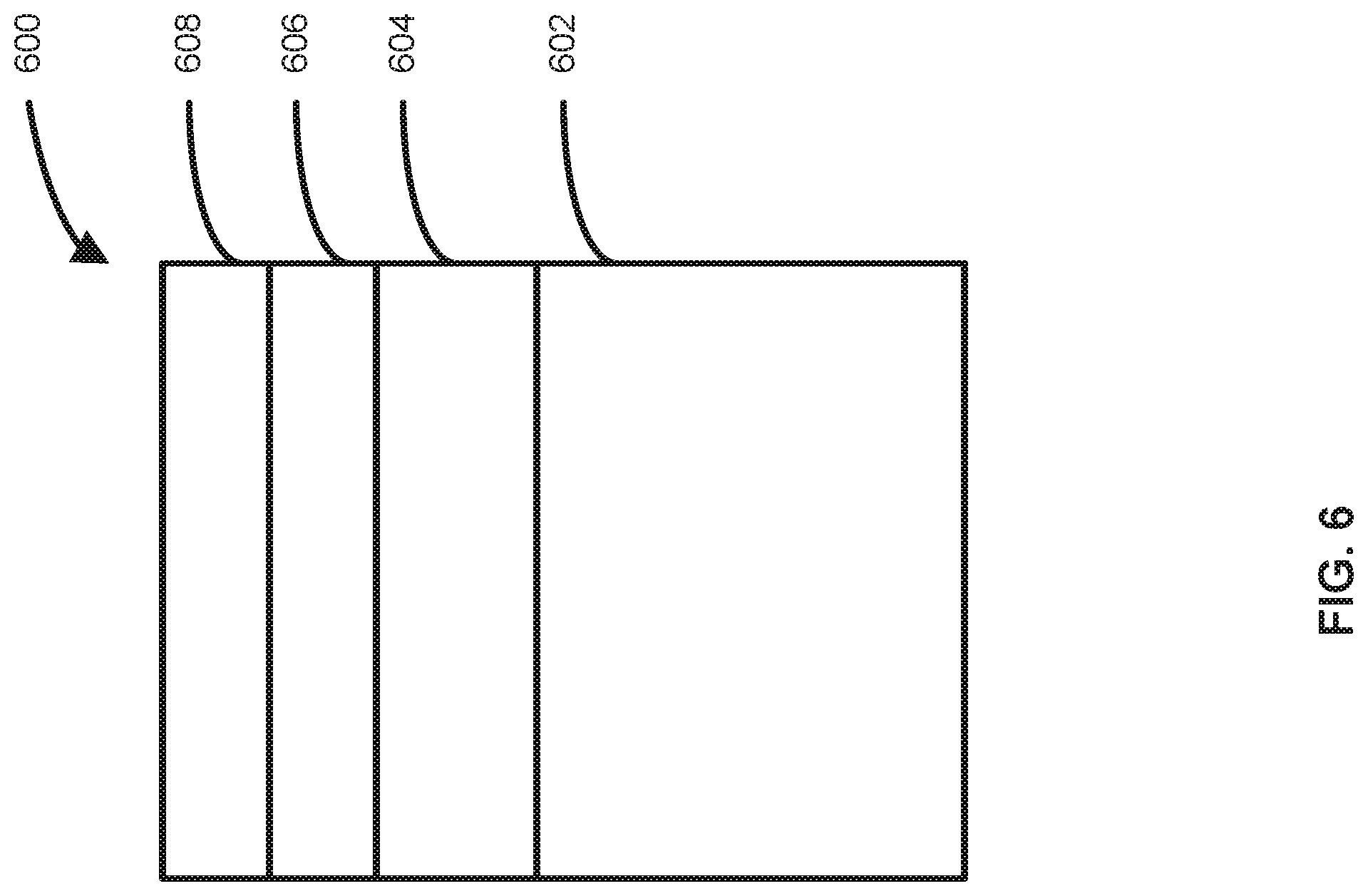
[0095] FIG. 6 illustrates a portion of a device 600 in accordance with additional examples of the disclosure. Portion of a device 600 includes a substrate 602, a first doped semiconductor layer 604, a second doped semiconductor layer 606, and a conducting layer 608.
[0096] Substrate 602 can be or include any of the substrate material described herein. For example, substrate 602 can be the same as substrate 202 and/or structure 200.
[0097] First doped semiconductor layer 604 can be the same or similar to first doped semiconductor layer 302 described above. First doped semiconductor layer 604 can be used to form a first portion of a source or drain region of a field effect transistor (FET), such as a source or drain region of a FinFET or other FET device. Similarly, second doped semiconductor layer 606 can be the same or similar to second doped semiconductor layer 502 described above. Second doped semiconductor layer 606 can be used to form a second portion of the source or drain region of the FET. Use of second doped semiconductor layer 606 can reduce a contact resistance between conducting layer 608 and the underlying doped semiconductor layer.
[0098] Conducting layer 606 can include, for example, metal, such as titanium, nickel, cobalt, nickel platinum alloy, or the like. By way of particular examples, a contact resistance of a gallium doped p-type doped silicon germanium (e.g., SiGe:B:Ga) layer 606 can be lower than 10.sup.-9 .OMEGA..cm.sup.2 to about 5.times.10.sup.-10 .OMEGA..cm.sup.2, about 5.times.10.sup.-10 .OMEGA..cm.sup.2 to about 2.times.10.sup.-10 .OMEGA..cm.sup.2, or about 2.times.10.sup.-10 .OMEGA..cm.sup.2 to about 1.times.10.sup.-10 .OMEGA..cm.sup.2 without annealing.
[0099] FIG. 7 illustrates a system 700 in accordance with yet additional exemplary embodiments of the disclosure. System 700 can be used to perform a method as described herein and/or form a structure or device portion as described herein.
[0100] In the illustrated example, system 700 includes an optional substrate handling system 702, one or more reaction chambers 704, a gas injection system 706, and optionally a wall 708 disposed between reaction chamber(s) 704 and substrate handling system 702. System 700 can also include a first gas source 710, a second gas source 712, a third gas source 714, a fourth gas source 716, an exhaust source 726, and a controller 728.
[0101] Although illustrated with four gas sources 710-716, system 700 can include any suitable number of gas sources. Gas sources 710-716 can each include, for example, a precursor gas, such as a precursor (e.g., Group IV, p-type dopant precursors, and/or n-type dopant precursors) as described above, including mixtures of such precursors and/or mixtures of one or more precursors with a carrier gas, such as hydrogen, nitrogen, argon, helium or the like. Additionally or alternatively, one of gas sources 710-716 or another gas source can include an etchant, such as a halide--e.g., a chlorine-containing gas, such as hydrogen chloride and/or chlorine. Gas sources 710-716 can be coupled to reaction chamber 704 via lines 718-724, which can each include flow controllers, valves, heaters, and the like.
[0102] System 700 can include any suitable number of reaction chambers 704 and substrate handling systems 702. Further, one or more reaction chambers 704 can be or include a cross-flow, cold wall epitaxial reaction chamber.
[0103] Vacuum source 720 can include one or more vacuum pumps.
[0104] Controller 728 can be configured to perform various functions and/or steps as described herein. For example, controller 728 can be configured to control gas flow into the gas injection system to selectively form a first doped semiconductor layer overlying a first surface of a substrate relative to a second surface of the substrate and selectively form a second doped semiconductor layer overlying the first doped semiconductor layer, as described above. Controller 728 can include one or more microprocessors, memory elements, and/or switching elements to perform the various functions. Although illustrated as a single unit, controller 728 can alternatively comprise multiple devices. By way of examples, controller 728 can be used to control gas flow (e.g., by monitoring flow rates of precursors and/or other gases from sources 710-716 and/or controlling valves, motors, heaters, and the like). Further, when system 700 includes two or more reaction chambers, the two or more reaction chambers can be coupled to the same/shared controller.
[0105] During operation of reactor system 700, substrates, such as semiconductor wafers (not illustrated), are transferred from, e.g., substrate handling system 702, to reaction chamber 704. Once substrate(s) are transferred to reaction chamber 704, one or more gases from gas sources 710-716, such as precursors, dopants, carrier gases, and/or purge gases, are introduced into reaction chamber 704 via gas injection system 706. Gas injection system 706 can be used to meter and control gas flow of one or more gases (e.g., from one or more gas sources 710-716) during substrate processing and to provide desired flows of such gas(es) to multiple sites within reaction chamber 704.
[0106] With reference to FIG. 8, a substrate (or structure) provided during step (802) can include a first area comprising a first material (e.g., (mono)-crystalline bulk material) and a second area comprising a second material (e.g., non-monocrystalline material). The first material can include a monocrystalline surface; the second area can include a non-monocrystalline surface, such as a polycrystalline surface or an amorphous surface. The monocrystalline surface may be a monocrystalline silicon, germanium, or silicon germanium surface, and may comprise one or more doping elements, such as p-type doping elements, such as boron or gallium.
[0107] FIG. 8 illustrates a selective deposition method (800) in accordance with exemplary embodiments of the disclosure. The method (800) includes steps of providing a substrate within a reaction chamber (step 802), selectively depositing a first doped semiconductor layer (step 803), selectively depositing a second doped semiconductor layer (step 804). Optionally, the method comprises a step of etching a part of the first doped semiconductor layer (step 811) in order to remove parasitic nuclei that may have been deposited on the second area. Optionally the step of depositing the first doped semiconductor layer (803) and the step of etching a part of the first doped semiconductor layer (811) are repeated (loop 810). Optionally, the method comprises a further step of first depositing a capping layer (805) and then etching the capping layer (808) and ending (step 812). The capping layer may comprise a silicon layer, e.g., a silicon layer doped with boron and/or gallium.
[0108] As a non-limiting example, the reaction chamber used during the step (802) of providing the substrate may comprise a reaction chamber of a chemical vapor deposition system. This notwithstanding, other reaction chambers and alternative chemical vapor deposition systems may also be utilized to perform the embodiments of the present disclosure. The reaction chamber can be a stand-alone reaction chamber or part of a cluster tool.
[0109] The substrate providing step (802) can include heating the substrate to a desired deposition temperature within the reaction chamber. In some embodiments of the disclosure, the substrate providing step (802) includes heating the substrate to a temperature of less than approximately 600.degree. C., or even to a temperature of less than approximately 550.degree. C. For example, in some embodiments of the disclosure, heating the substrate to a deposition temperature may comprise heating the substrate to a temperature of at least 350.degree. C. to at most 550.degree. C. The deposition temperature is maintained throughout the step of depositing the boron and gallium doped silicon germanium layer (804), the optional capping step (805), and the optional etching steps (808,811).
[0110] In an exemplary embodiment, described is a selective deposition method. The selective deposition method comprises providing a substrate within a reaction chamber. The substrate comprises a surface comprising a first area comprising a first material and a second area comprising a second material. The method further comprises selectively and epitaxially depositing a first doped semiconductor layer overlying the first material; and selectively and epitaxially depositing a second doped semiconductor layer overlying the first doped semiconductor layer. The first material may comprise a doped or undoped monocrystalline material, for example a material selected from the list consisting of silicon (Si), silicon germanium (SiGe), germanium tin (GeSn), silicon germanium tin (SiGeSn), and germanium (Ge). The second material may comprise a non-monocrystalline dielectric material, for example a material selected from silicon oxide, silicon nitride, silicon oxynitride, silicon carbide, silicon oxycarbide, and mixtures thereof.
[0111] The first doped semiconductor layer may suitably comprise boron-doped silicon germanium. Alternatively, the first doped semiconductor layer comprises a lower part and an upper part. The lower part may comprise p-type germanium, and the upper part comprises p-type silicon germanium, e.g., boron-doped silicon germanium. Without the invention being bound to any particular theory or mode of operation, it is believed that by growing gallium-doped germanium (Ge:Ga), or alternatively boron and gallium doped germanium (Ge:BGa) prior to growing p-type silicon germanium such as boron-doped silicon germanium SiGe:B has the following effect: all, or a substantial part of the gallium used to dope the germanium layer will diffuse to the SiGe:B layer surface, while any carbon impurities incorporated in the Ge:Ga layer, e.g., due to the use of an organometallic Ga precursor, carbon may become trapped inside the SiGe:B layer. Thus, the amount of carbon at the surface of the SiGe:B layer may be reduced, which can help with reducing contact resistance when contacts are formed on the SiGe:B layer.
[0112] In some embodiments, the p-type germanium comprises boron and gallium doped germanium. The p-type silicon germanium may comprise boron-doped silicon germanium.
[0113] In some embodiments, the second doped semiconductor layer comprises p-type silicon, e.g., boron-doped silicon or boron and gallium-doped silicon.
[0114] The step of selectively depositing the first doped semiconductor layer may comprise simultaneously flowing a precursor and an etchant to the reaction chamber. Alternatively, selectively depositing the first doped semiconductor layer and/or selectively depositing the second doped semiconductor layer comprises alternating cycles of flowing one or more precursors to the reaction chamber, and of flowing an etchant to the reaction chamber. Exemplary etchants include elementary halogens or halogen-containing compounds, such as hydrogen chloride and/or chlorine.
[0115] The precursors and/or etchants used during deposition of the first and second doped semiconductor layers may be the same, e.g., when the first and second doped semiconductor layers have the same components, but in a different concentration. Alternatively, the first and second doped semiconductor layers may be grown using different precursors and/or etchants.
[0116] In some embodiments, the step of selectively depositing the first doped semiconductor layer comprises depositing a p-type doped silicon germanium layer, and the step of selectively depositing the second doped semiconductor layer comprises selectively depositing a gallium-doped layer overlying the p-type doped silicon germanium layer. The gallium-doped layer may additionally be doped with boron, and my comprise silicon, germanium, or both.
[0117] In another exemplary embodiment, a transistor device is described. The transistor device comprises a source region and a drain region which are both formed using a method as described herein. Preferably, the source and drain regions are formed simultaneously, i.e., in a single deposition step. The source region and/or the drain region may comprise a second doped semiconductor layer comprising about 1.times.10.sup.19 charge carriers/cm.sup.3 to about 5.times.10.sup.21 charge carriers/cm.sup.3, e.g., 2 to 3.times.10.sup.21 charge carriers/cm.sup.3. Additionally or alternatively, the source region and/or the drain region may comprise a second doped semiconductor layer comprising about 10% to about 90%, or about 35% to about 70%, or about 40% to about 50% silicon. Additionally or alternatively, the second doped semiconductor layer may comprise about 10% to about 90%, or about 65% to about 30%, or about 60% to about 50% germanium. Additionally or alternatively, the source region and/or the drain region may comprise a first doped semiconductor layer having a thickness of between about 1 nm and 20 nm. Additionally or alternatively, the source region and/or the drain region may comprise a second doped semiconductor layer having a thickness between about 1 nm and 20 nm.
[0118] Further described herein is a system comprising one or more reaction chambers; a gas injection system fluidly coupled to at least one of the one or more reaction chambers; a first gas source; a second gas source; a third gas source; an exhaust source; and a controller. Suitably, the controller may be configured to control gas flow into the gas injection system to selectively form a first doped semiconductor layer overlying a first surface of a substrate relative to a second surface of the substrate and selectively form a second doped semiconductor layer overlying the first doped semiconductor layer. In some embodiments, the controller is configured to perform a step of etching the first doped semiconductor layer overlying the second surface in the one or more reaction chambers. The first gas source may comprise a silicon precursor source, the second gas source may comprise a germanium precursor source, and the third gas source may comprise a boron precursor source. The system may further comprise a fourth gas source, which comprises a gallium precursor source.
[0119] The example embodiments of the disclosure described above do not limit the scope of the invention, since these embodiments are merely examples of the embodiments of the invention, which is defined by the appended claims and their legal equivalents. Any equivalent embodiments are intended to be within the scope of this invention. Indeed, various modifications of the disclosure, in addition to those shown and described herein, such as alternative useful combinations of the elements described, may become apparent to those skilled in the art from the description. Such modifications and embodiments are also intended to fall within the scope of the appended claims.
* * * * *
D00000
D00001
D00002
D00003
D00004
D00005
D00006
D00007
D00008
XML
uspto.report is an independent third-party trademark research tool that is not affiliated, endorsed, or sponsored by the United States Patent and Trademark Office (USPTO) or any other governmental organization. The information provided by uspto.report is based on publicly available data at the time of writing and is intended for informational purposes only.
While we strive to provide accurate and up-to-date information, we do not guarantee the accuracy, completeness, reliability, or suitability of the information displayed on this site. The use of this site is at your own risk. Any reliance you place on such information is therefore strictly at your own risk.
All official trademark data, including owner information, should be verified by visiting the official USPTO website at www.uspto.gov. This site is not intended to replace professional legal advice and should not be used as a substitute for consulting with a legal professional who is knowledgeable about trademark law.