High-voltage Devices
Kaner; Richard Barry ; et al.
U.S. patent application number 17/110397 was filed with the patent office on 2021-04-22 for high-voltage devices. The applicant listed for this patent is The Regents of the University of California. Invention is credited to Maher F. El-Kady, Richard Barry Kaner.
| Application Number | 20210118628 17/110397 |
| Document ID | / |
| Family ID | 1000005303326 |
| Filed Date | 2021-04-22 |


View All Diagrams
| United States Patent Application | 20210118628 |
| Kind Code | A1 |
| Kaner; Richard Barry ; et al. | April 22, 2021 |
HIGH-VOLTAGE DEVICES
Abstract
The present disclosure provides supercapacitors that may avoid the shortcomings of current energy storage technology. Provided herein are supercapacitor devices, and methods of fabrication thereof comprising the manufacture or synthesis of an active material on a current collector and/or the manufacture of supercapacitor electrodes to form planar and stacked arrays of supercapacitor electrodes and devices. Prototype supercapacitors disclosed herein may exhibit improved performance compared to commercial supercapacitors. Additionally, the present disclosure provides a simple, yet versatile technique for the fabrication of supercapacitors through masking and etching.
| Inventors: | Kaner; Richard Barry; (Pacific Palisades, CA) ; El-Kady; Maher F.; (Los Angeles, CA) | ||||||||||
| Applicant: |
|
||||||||||
|---|---|---|---|---|---|---|---|---|---|---|---|
| Family ID: | 1000005303326 | ||||||||||
| Appl. No.: | 17/110397 | ||||||||||
| Filed: | December 3, 2020 |
Related U.S. Patent Documents
| Application Number | Filing Date | Patent Number | ||
|---|---|---|---|---|
| 16692123 | Nov 22, 2019 | 10892109 | ||
| 17110397 | ||||
| 15410404 | Jan 19, 2017 | 10614968 | ||
| 16692123 | ||||
| 62286126 | Jan 22, 2016 | |||
| Current U.S. Class: | 1/1 |
| Current CPC Class: | H01G 11/86 20130101; H01G 11/30 20130101; Y02E 60/13 20130101; H01G 11/60 20130101; H01G 11/68 20130101; H01G 11/70 20130101; H01G 11/26 20130101; H01G 11/28 20130101 |
| International Class: | H01G 11/60 20060101 H01G011/60; H01G 11/68 20060101 H01G011/68; H01G 11/30 20060101 H01G011/30; H01G 11/28 20060101 H01G011/28; H01G 11/26 20060101 H01G011/26; H01G 11/86 20060101 H01G011/86; H01G 11/70 20060101 H01G011/70 |
Claims
1. A supercapacitor device comprising: an array of electrodes, wherein each electrode comprises: a current collector; and an active material directly on a portion of a first surface of the current collector, wherein the active material comprises two or more corrugated carbon layers, each corrugated carbon layer having two or more of parallel ridges and furrows.
2. The supercapacitor device of claim 1, further comprising the active material directly on a portion of a second surface of the current collector.
3. The supercapacitor device of claim 1, wherein each electrode in the array of electrodes is separated from a subsequent electrode by a gap.
4. The supercapacitor device of claim 1, wherein the current collector comprises a metal film, a polymeric film, or any combination thereof, wherein the metal film comprises silver, copper, gold, aluminum, calcium, tungsten, zinc, brass, bronze, nickel, lithium, iron, platinum, tin, carbon steel, lead, titanium, stainless steel, mercury, chromium, gallium arsenide, or any combination thereof, and wherein the polymeric film comprises polyfluorene, polyphenylene, polypyrene, polyazulene, polynaphthalene, polyacetylene, poly p-phenylene vinylene, polypyrrole, polycarbazole, polyindole, polyazepinem, polyaniline, polythiophene, poly 3,4-ethylenedioxythiophene, poly p-phenylene sulfide, polyacetylene, or any combination thereof.
5. The supercapacitor device of claim 1, wherein the active material comprises carbon, activated carbon, graphene, polyaniline, polythiophene, an interconnected corrugated carbon-based network (ICCN), or any combination thereof.
6. The supercapacitor device of claim 1, wherein the active material has a specific surface area of from about 250 meters squared per gram to about 3,500 meters squared per gram.
7. The supercapacitor device of claim 1, wherein the active material has a conductivity of from about 750 siemens/meter to about 3,000 siemens/meter.
8. The supercapacitor device of claim 1, wherein the array of electrodes is a two-dimensional planar array of electrodes.
9. The supercapacitor device of claim 8, further comprising an aqueous electrolyte, wherein the number of electrodes is 5, provided that a produced voltage potential across the array of electrodes is from 2.5 V to 10 V.
10. The supercapacitor device of claim 8, further comprising an electrolyte comprising tetraethyl ammonium tetrafluoroborate (TEABF4) in acetonitrile, wherein the number of electrodes is 5, provided that a voltage potential produced across the array of electrodes is from 6 V to 24 V.
11. The supercapacitor device of claim 8, further comprising an aqueous electrolyte, wherein the number of electrodes is 180, provided that a voltage potential produced across the array of electrodes is from 100 V to 360 V.
12. The supercapacitor device of claim 8, further comprising an electrolyte comprising tetraethyl ammonium tetrafluoroborate (TEABF4) in acetonitrile, wherein the number of electrodes is 72, provided that a voltage potential produced across the array of electrodes is from 100 V to 360 V.
13. The supercapacitor device of claim 1, wherein the array of electrodes is a stacked array of electrodes.
14. The supercapacitor device of claim 13, further comprising at least one or more of a separator and a support between a pair of adjacent electrodes.
15. The supercapacitor device of claim 13, wherein the stacked array of electrodes comprises one or more single-sided electrodes and one or more double-sided electrodes.
16. The supercapacitor device of claim 1, further comprising an electrolyte, wherein the electrolyte is a liquid, a solid, a gel, or any combination thereof comprising a polymer, silica, fumed silica, fumed silica nano-powder, 1-butyl-3-methylimidazolium bis(trifluoromethylsulfonyl)imide, phosphoric acid, tetraethyl ammonium tetrafluoroborate (TEABF4), acetonitrile, 1-ethyl-3-methylimidazoliumtetrafluoroborate, ethanolammonium nitrate, a dicarboxylate, a prostaglandin, adenosine monophosphate, guanosine monophosphate, a p-aminohippurate, polysiloxane, polyphosphazene, potassium hydroxide, polyvinyl alcohol, or any combination thereof.
17. The supercapacitor device of claim 1, wherein the array of electrodes comprises a linear array of electrodes comprising at least one isobilateral electrode and at least two anisobilateral electrodes.
18. A method of fabricating an array of electrodes comprising: a) applying an active material directly onto a portion of a first surface of a current collector, wherein the active material comprises two or more corrugated carbon layers, each corrugated carbon layer having two or more of parallel ridges and furrows; and b) drying the active material on the current collector; provided that each electrode is separated from a subsequent electrode by a gap.
19. The method of claim 18, further comprising: c) applying the active material directly onto a portion of a second surface of the current collector; and d) drying the active material on the current collector.
20. The method of claim 19, wherein at least one or more of a tape and a mask shields a portion of the second surface of the current collector to thereby prevent application of the active material onto the shielded portion of the second surface of the current collector.
Description
CROSS-REFERENCE
[0001] This application is a continuation of U.S. application Ser. No. 16/692,123, filed Nov. 22, 2020, which is a continuation of U.S. application Ser. No. 15/410,404, filed Jan. 19, 2017, now U.S. Pat. No. 10,614,968, which claims the benefit of U.S. Provisional Application No. 62/286,126, filed Jan. 22, 2016, which applications are incorporated herein by reference in their entireties.
BACKGROUND
[0002] The development of high performance energy storage devices has gained significant attention in a broad range of applications. While normal electronic devices progress rapidly, according to Moore's law, batteries have advanced only slightly, mainly due to the limitations of current materials' energy densities and capacities.
SUMMARY
[0003] The inventors have identified that batteries with a reduced charge time and an increased charge density have a profound effect on the design and use of portable electronics and renewable energy devices. Provided herein are methods, devices and systems of supercapacitors. The methods may include the manufacture (or synthesis) of an active material on a current collector and/or the manufacture of supercapacitor electrodes. Some embodiments provide methods, devices and systems for the manufacture (or synthesis) of planar and stacked arrays of electrodes and/or for the manufacture (or synthesis) of supercapacitors.
[0004] A first aspect of the disclosure provided herein is supercapacitor device comprising an array of electrodes, wherein each electrode comprises a current collector; and an active material on a portion of first surface of the current collector.
[0005] In some embodiments, the supercapacitor of the first aspect further comprises the active material on a portion of a second surface of the current collector.
[0006] In some embodiments, each electrode in the array is separated from a subsequent electrode by a gap.
[0007] In some embodiments, the current collector comprises a metal film or a polymeric film or any combination thereof, wherein the metal film comprises silver, copper, gold, aluminum, calcium, tungsten, zinc, tungsten, brass, bronze, nickel, lithium, iron, platinum, tin, carbon steel, lead, titanium, stainless steel, mercury, chromium, gallium arsenide or any combination thereof, and wherein the polymeric film comprises polyfluorene, polyphenylene, polypyrene, polyazulene, polynaphthalene, polyacetylene, poly p-phenylene vinylene, polypyrrole, polycarbazole, polyindole, polyazepinem, polyaniline, polythiophene, poly 3,4-ethylenedioxythiophene, poly p-phenylene sulfide, polyacetylene, poly p-phenylene vinylene or any combination thereof.
[0008] In some embodiments, the active material comprises two or more separated and interconnected layers. In some embodiments, the active material comprises carbon, activated carbon, graphene, polyaniline, polythiophene, an interconnected corrugated carbon-based network (ICCN) or any combination thereof. In some embodiments, the active material has a surface density of from about 250 meters squared per gram to about 3,500 meters squared per gram. In some embodiments, the active material has a conductivity of from about 750 siemens/meter to about 3,000 siemens/meter.
[0009] In some embodiments, the array of electrodes is a planar array of electrodes. In further such embodiments, the electrolyte is aqueous wherein the number of electrodes is about 5, and the produced voltage potential across the array of electrodes is from about 2.5 V to about 10 V. In further such embodiments, the electrolyte comprises tetraethyl ammonium tetrafluoroborate (TEABF.sub.4) in acetonitrile wherein the number of electrodes is about 5, and the voltage potential produced across the array of electrodes is from about 6 V to about 24 V. In further such embodiments, the electrolyte is aqueous, wherein the number of electrodes is about 180, and the voltage potential produced across the array of electrodes is from about 100 V to about 360 V. In further such embodiments the electrolyte comprises tetraethyl ammonium tetrafluoroborate (TEABF.sub.4) in acetonitrile, wherein the number of electrodes is about 72, and the voltage potential produced across the array pf electrodes is from about 100 V to about 360 V.
[0010] In some embodiments, the array of electrodes is a stacked array of electrodes.
[0011] In some embodiments, the supercapacitor device of the first aspect further comprises at least one or more of a separator and a support, wherein the at least one or more of a separator and a support is positioned between a pair of adjacent electrodes.
[0012] In some embodiments, the supercapacitor device of the first aspect further comprises an electrolyte, wherein the electrolyte is a liquid, a solid, a gel, or any combination thereof comprising a polymer, silica, fumed silica, fumed silica nano-powder,1-butyl-3-methylimidazolium bis(trifluoromethylsulfonyl)imide, phosphoric acid, tetraethyl ammonium tetrafluoroborate (TEABF.sub.4), acetonitrile, 1-ethyl-3-methylimidazoliumtetrafluoroborate, ethanolammonium nitrate, a dicarboxylate, a prostaglandin, adenosine monophosphate, guanosine monophosphate, a p-aminohippurate, polysiloxane, polyphosphazene, potassium hydroxide, polyvinyl alcohol or any combination thereof.
[0013] A second aspect of the disclosure provided herein is a method of fabricating a supercapacitor comprising, fabricating an array of electrodes comprising: applying an active material onto a portion of the first surface of the current collector; and drying the active material on the current collector, wherein each electrode is separated from a subsequent electrode by a gap.
[0014] In some embodiments, the method of the second aspect further comprises applying an active material onto a portion of the second surface of the current collector; and drying the active material on the current collector.
[0015] In some embodiments, at least one or more of a tape and a mask, shields a portion of the substrate to thereby prevent application of an active material onto the shielded portion of the substrate.
[0016] In some embodiments, the active material is applied in the form of a slurry. In some embodiments, the slurry is applied to the substrate by a doctor blade. In some embodiments, the process of applying an active material onto the first surface of the current collector and the process of applying an active material onto the second surface of the current collector are performed simultaneously.
[0017] In some embodiments, the drying of the active material on the current collector occurs at a temperature of from about 40.degree. C. to about 160.degree. C. In some embodiments, the drying of the active material on the current collector current collector occurs over a period of time from about 6 hours to about 24 hours.
[0018] In some embodiments, the electrode array comprises a planar electrode array. In some embodiments, planar electrode array is fabricated by etching or cutting the active material and the current collector.
[0019] In some embodiments, the electrode array comprises a stacked electrode array.
[0020] In some embodiments, the method of the second aspect further comprises positioning at least one or more of a separator and a support, between a pair of consecutive electrodes.
[0021] In some embodiments, the method of the second aspect further comprises dispersing an electrolyte on the array of electrodes; encasing the array of electrodes in a sheath; and inserting the encased array of electrodes into a housing.
[0022] In some embodiments, the electrolyte is a liquid, a solid, a gel, or any combination thereof comprising a polymer, silica, fumed silica, fumed silica nano-powder,1-butyl-3-methylimidazolium bis(trifluoromethylsulfonyl)imide, phosphoric acid, tetraethyl ammonium tetrafluoroborate (TEABF.sub.4), acetonitrile, 1-ethyl-3-methylimidazoliumtetrafluoroborate, ethanolammonium nitrate, a dicarboxylate, a prostaglandin, adenosine monophosphate, guanosine monophosphate, a p-aminohippurate, polysiloxane, polyphosphazene, potassium hydroxide, polyvinyl alcohol or any combination thereof.
BRIEF DESCRIPTION OF THE DRAWINGS
[0023] The novel features of the disclosure are set forth with particularity in the appended claims. A better understanding of the features and advantages of the present disclosure will be obtained by reference to the following detailed description that sets forth illustrative embodiments, in which the principles of the disclosure are utilized, and the accompanying drawings or figures (also "FIG." and "FIGs." herein), of which:
[0024] FIGS. 1A-D show exemplary illustrations of supercapacitors having multiple electrodes.
[0025] FIG. 2 shows an exemplary illustration of a supercapacitor having 180 cells.
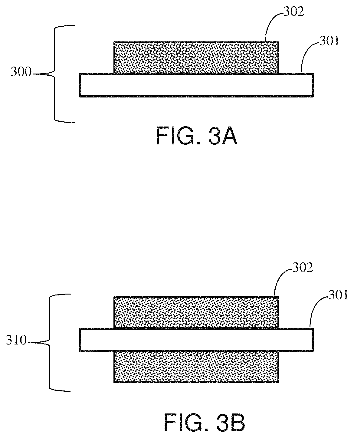
[0026] FIGS. 3A-B show exemplary illustrations of a single-sided electrode and a double-sided electrode.
[0027] FIGS. 4A-B show exemplary front and top cross-sectional illustrations of an assembled supercapacitor.
[0028] FIGS. 5A-B show an exemplary front cross-sectional illustration of an assembled supercapacitor with supports, and an exemplary illustration of a supported double-sided electrode.
[0029] FIGS. 6A-C show exemplary exploded, perspective and top view illustrations of a packaged single-cell supercapacitor.
[0030] FIG. 7 shows an exemplary image of the application of an active material onto a current collector.
[0031] FIG. 8 shows an exemplary image of the active material applied on the current collector.
[0032] FIGS. 9A-B show exemplary images of the electrode after drying and tape removal.
[0033] FIG. 10 shows an exemplary image of the fabrication of a patterned planar electrode.
[0034] FIG. 11 shows an exemplary image of a high-voltage supercapacitor during electrochemical testing.
[0035] FIGS. 12A-E show cyclic voltammetry (CV) graphs of an exemplary supercapacitor device at different scan rates.
[0036] FIG. 13 shows an overlay of the cyclic voltammetry (CV) graphs of an exemplary supercapacitor device at different scan rates.
[0037] FIG. 14 shows the charge and discharge performance of an exemplary supercapacitor under a constant current.
[0038] FIG. 15 shows the Warburg impedance of an exemplary supercapacitor.
DETAILED DESCRIPTION OF THE INVENTION
[0039] The inventors have recognized a need for an improved design of, and the integration of hybrid materials into, microsupercapacitors, to simplify the microfabrication of 3D microelectrodes with micrometer separations.
[0040] The present disclosure provides a simple, yet versatile technique for the fabrication of supercapacitors. The present disclosure provides a method for the preparation and/or integration of supercapacitors for high voltage applications. In some embodiments, the present disclosure provides a method for the direct preparation and integration of supercapacitors for high voltage applications. The supercapacitors may comprise an array of separate electrochemical cells. In some embodiments, the array of separate electrochemical electrodes may be directly fabricated in the same plane and in one step. This configuration may provide very good control over the voltage and current output. In some embodiments, the array may be integrated with solar electrodes for efficient solar energy harvesting and storage. In some embodiments, the devices are integrated supercapacitors for high voltage applications.
[0041] An aspect of the disclosure provides a supercapacitor device comprising an array of electrodes, wherein each electrode comprises a current collector; and an active material on a portion of first surface of the current collector. In some embodiments, the current collector comprises active material on a portion of a second surface of the current collector. In some embodiments, an electrode in the array is separated from a subsequent electrode by a gap.
[0042] In some embodiments, the active material comprises carbon, activated carbon, graphene, polyaniline, polythiophene, an interconnected corrugated carbon-based network (ICCN) or any combination thereof.
[0043] In some embodiments, the current collector comprises a metal film or a polymeric film or any combination thereof. In some embodiments, the metal film comprises silver, copper, gold, aluminum, calcium, tungsten, zinc, tungsten, brass, bronze, nickel, lithium, iron, platinum, tin, carbon steel, lead, titanium, stainless steel, mercury, chromium, gallium arsenide or any combination thereof. In some embodiments, the polymeric film comprises polyfluorene, polyphenylene, polypyrene, polyazulene, polynaphthalene, polyacetylene, poly p-phenylene vinylene, polypyrrole, polycarbazole, polyindole, polyazepinem, polyaniline, polythiophene, poly 3,4-ethylenedioxythiophene, poly p-phenylene sulfide, polyacetylene, poly p-phenylene vinylene or any combination thereof.
[0044] In some embodiments, the thickness of the current collector is from about 50 nanometers to about 200 nanometers. In some embodiments, the thickness of the current collector is at least about 50 nanometers. In some embodiments, the thickness of the current collector is at most about 200 nanometers. In some embodiments, thickness of the current collector is about 50 nanometers to about 75 nanometers, about 50 nanometers to about 100 nanometers, about 50 nanometers to about 125 nanometers, about 50 nanometers to about 150 nanometers, about 50 nanometers to about 175 nanometers, about 50 nanometers to about 200 nanometers, about 75 nanometers to about 100 nanometers, about 75 nanometers to about 125 nanometers, about 75 nanometers to about 150 nanometers, about 75 nanometers to about 175 nanometers, about 75 nanometers to about 200 nanometers, about 100 nanometers to about 125 nanometers, about 100 nanometers to about 150 nanometers, about 100 nanometers to about 175 nanometers, about 100 nanometers to about 200 nanometers, about 125 nanometers to about 150 nanometers, about 125 nanometers to about 175 nanometers, about 125 nanometers to about 200 nanometers, about 150 nanometers to about 175 nanometers, about 150 nanometers to about 200 nanometers, or about 175 nanometers to about 200 nanometers.
[0045] In some embodiments, the active material comprises two or more separated and interconnected layers. In some embodiments, a layer is corrugated. In some embodiments, a layer is one atom thick.
[0046] In some embodiments, a portion of the layers are separated by a distance of at least about 1 nanometer (nm). In some embodiments, a portion of the layers are separated by a distance of at most about 150 nm. In some embodiments, a portion of the layers are separated by a distance of about 1 nm to about 150 nm. In some embodiments, a portion of the layers are separated by a distance of about 1 nm to about 5 nm, about 1 nm to about 10 nm, about 1 nm to about 25 nm, about 1 nm to about 50 nm, about 1 nm to about 100 nm, about 1 nm to about 150 nm, about 5 nm to about 10 nm, about 5 nm to about 25 nm, about 5 nm to about 50 nm, about 5 nm to about 100 nm, about 5 nm to about 150 nm, about 10 nm to about 25 nm, about 10 nm to about 50 nm, about 10 nm to about 100 nm, about 10 nm to about 150 nm, about 25 nm to about 50 nm, about 25 nm to about 100 nm, about 25 nm to about 150 nm, about 50 nm to about 100 nm, about 50 nm to about 150 nm, or about 100 nm to about 150 nm.
[0047] In some embodiments, the active material has a surface density of at least about 250 meters squared per gram (m.sup.2/g). In some embodiments, the active material has a surface density of at most about 3,500 m.sup.2/g. In some embodiments, the active material has a surface density of about 250 m.sup.2/g to about 3,500 m.sup.2/g. In some embodiments, the active material has a surface density of about 250 m.sup.2/g to about 500 m.sup.2/g, about 250 m.sup.2/g to about 750 m.sup.2/g, about 250 m.sup.2/g to about 1,000 m.sup.2/g, about 250 m.sup.2/g to about 1,500 m.sup.2/g, about 250 m.sup.2/g to about 2,000 m.sup.2/g, about 250 m.sup.2/g to about 2,500 m.sup.2/g, about 250 m.sup.2/g to about 3,000 m.sup.2/g, about 250 m.sup.2/g to about 3,500 m.sup.2/g, about 500 m.sup.2/g to about 750 m.sup.2/g, about 500 m.sup.2/g to about 1,000 m.sup.2/g, about 500 m.sup.2/g to about 1,500 m.sup.2/g, about 500 m.sup.2/g to about 2,000 m.sup.2/g, about 500 m.sup.2/g to about 2,500 m.sup.2/g, about 500 m.sup.2/g to about 3,000 m.sup.2/g, about 500 m.sup.2/g to about 3,500 m.sup.2/g, about 750 m.sup.2/g to about 1,000 m.sup.2/g, about 750 m.sup.2/g to about 1,500 m.sup.2/g, about 750 m.sup.2/g to about 2,000 m.sup.2/g, about 750 m.sup.2/g to about 2,500 m.sup.2/g, about 750 m.sup.2/g to about 3,000 m.sup.2/g, about 750 m.sup.2/g to about 3,500 m.sup.2/g, about 1,000 m.sup.2/g to about 1,500 m.sup.2/g, about 1,000 m.sup.2/g to about 2,000 m.sup.2/g, about 1,000 m.sup.2/g to about 2,500 m.sup.2/g, about 1,000 m.sup.2/g to about 3,000 m.sup.2/g, about 1,000 m.sup.2/g to about 3,500 m.sup.2/g, about 1,500 m.sup.2/g to about 2,000 m.sup.2/g, about 1,500 m.sup.2/g to about 2,500 m.sup.2/g, about 1,500 m.sup.2/g to about 3,000 m.sup.2/g, about 1,500 m.sup.2/g to about 3,500 m.sup.2/g, about 2,000 m.sup.2/g to about 2,500 m.sup.2/g, about 2,000 m.sup.2/g to about 3,000 m.sup.2/g, about 2,000 m.sup.2/g to about 3,500 m.sup.2/g, about 2,500 m.sup.2/g to about 3,000 m.sup.2/g, about 2,500 m.sup.2/g to about 3,500 m.sup.2/g, or about 3,000 m.sup.2/g to about 3,500 m.sup.2/g.
[0048] In some embodiments, active material has a conductivity of at least about 750 siemens/meter (S/m). In some embodiments, active material has a conductivity of at most about 3,000 S/m. In some embodiments, active material has a conductivity of about 750 S/m to about 3,000 S/m. In some embodiments, active material has a conductivity of about 750 S/m to about 1,000 S/m, about 750 S/m to about 1,500 S/m, about 750 S/m to about 2,000 S/m, about 750 S/m to about 2,500 S/m, about 750 S/m to about 3,000 S/m, about 1,000 S/m to about 1,500 S/m, about 1,000 S/m to about 2,000 S/m, about 1,000 S/m to about 2,500 S/m, about 1,000 S/m to about 3,000 S/m, about 1,500 S/m to about 2,000 S/m, about 1,500 S/m to about 2,500 S/m, about 1,500 S/m to about 3,000 S/m, about 2,000 S/m to about 2,500 S/m, about 2,000 S/m to about 3,000 S/m, or about 2,500 S/m to about 3,000 S/m.
[0049] In some embodiments, the two or more electrodes are arranged in an array. In some embodiments, each electrode in the array is separated from a subsequent electrode by a gap.
[0050] In some embodiments, the array is a planar array. In some embodiments, the number of electrodes is at least about 2.
[0051] In some embodiments, the width of the gap at least about 10 .mu.m. In some embodiments, the width of the gap at most about 2,000 .mu.m. In some embodiments, the width of the gap about from 10 .mu.m to about 2,000 .mu.m. In some embodiments, the width of the gap about 10 .mu.m to about 25 .mu.m, about 10 .mu.m to about 50 .mu.m, about 10 .mu.m to about 100 .mu.m, about 10 .mu.m to about 500 .mu.m, about 10 .mu.m to about 1,000 .mu.m, about 10 .mu.m to about 1,500 .mu.m, about 10 .mu.m to about 2,000 .mu.m, about 25 .mu.m to about 50 .mu.m, about 25 .mu.m to about 100 .mu.m, about 25 .mu.m to about 500 .mu.m, about 25 .mu.m to about 1,000 .mu.m, about 25 .mu.m to about 1,500 .mu.m, about 25 .mu.m to about 2,000 .mu.m, about 50 .mu.m to about 100 .mu.m, about 50 .mu.m to about 500 .mu.m, about 50 .mu.m to about 1,000 .mu.m, about 50 .mu.m to about 1,500 .mu.m, about 50 .mu.m to about 2,000 .mu.m, about 100 .mu.m to about 500 .mu.m, about 100 .mu.m to about 1,000 .mu.m, about 100 .mu.m to about 1,500 .mu.m, about 100 .mu.m to about 2,000 .mu.m, about 500 .mu.m to about 1,000 .mu.m, about 500 .mu.m to about 1,500 .mu.m, about 500 .mu.m to about 2,000 .mu.m, about 1,000 .mu.m to about 1,500 .mu.m, about 1,000 .mu.m to about 2,000 .mu.m, or about 1,500 .mu.m to about 2,000 .mu.m.
[0052] In some embodiments, the supercapacitor device further comprises an electrolyte. In some embodiments, the electrolyte is a liquid, a solid, a gel, or any combination thereof. In some embodiments, the electrolyte comprises a polymer, silica, 1-butyl-3-methylimidazolium bis(trifluoromethylsulfonyl)imide, phosphoric acid, tetraethyl ammonium tetrafluoroborate (TEABF.sub.4), acetonitrile, 1-ethyl-3-methylimidazoliumtetrafluoroborate, ethanolammonium nitrate, a dicarboxylate, a prostaglandin, adenosine monophosphate, guanosine monophosphate, a p-aminohippurate, polysiloxane, polyphosphazene, potassium hydroxide, polyvinyl alcohol or any combination thereof. In some embodiments, the silica is fumed silica. In some embodiments, the silica is fumed silica and/or is in the form of a nano-powder.
[0053] In some embodiments, the electrolyte is aqueous and wherein the number of electrodes is about 5. In this embodiment, the produced voltage potential across the array of electrodes is at least about 2.5 volts (V). In some embodiments, produced voltage potential across the array of electrodes is at most about 10 V. In some embodiments, produced voltage potential across the array of electrodes is about 2.5 V to about 10 V. In some embodiments, produced voltage potential across the array of electrodes is about 2.5 V to about 3 V, about 2.5 V to about 4 V, about 2.5 V to about 5 V, about 2.5 V to about 6 V, about 2.5 V to about 8 V, about 2.5 V to about 10 V, about 3 V to about 4 V, about 3 V to about 5 V, about 3 V to about 6 V, about 3 V to about 8 V, about 3 V to about 10 V, about 4 V to about 5 V, about 4 V to about 6 V, about 4 V to about 8 V, about 4 V to about 10 V, about 5 V to about 6 V, about 5 V to about 8 V, about 5 V to about 10 V, about 6 V to about 8 V, about 6 V to about 10 V, or about 8 V to about 10 V.
[0054] In some embodiments, the electrolyte comprises tetraethyl ammonium tetrafluoroborate (TEABF.sub.4) in acetonitrile and wherein the number of electrodes is about 5. In this embodiment, the produced voltage potential across the array of electrodes is at least about 6 V. In some embodiments, produced voltage potential across the array of electrodes is at most about 24 V. In some embodiments, produced voltage potential across the array of electrodes is about 6 V to about 24 V. In some embodiments, produced voltage potential across the array of electrodes is about 6 V to about 8 V, about 6 V to about 10 V, about 6 V to about 12 V, about 6 V to about 14 V, about 6 V to about 16 V, about 6 V to about 18 V, about 6 V to about 20 V, about 6 V to about 22 V, about 6 V to about 24 V, about 8 V to about 10 V, about 8 V to about 12 V, about 8 V to about 14 V, about 8 V to about 16 V, about 8 V to about 18 V, about 8 V to about 20 V, about 8 V to about 22 V, about 8 V to about 24 V, about 10 V to about 12 V, about 10 V to about 14 V, about 10 V to about 16 V, about 10 V to about 18 V, about 10 V to about 20 V, about 10 V to about 22 V, about 10 V to about 24 V, about 12 V to about 14 V, about 12 V to about 16 V, about 12 V to about 18 V, about 12 V to about 20 V, about 12 V to about 22 V, about 12 V to about 24 V, about 14 V to about 16 V, about 14 V to about 18 V, about 14 V to about 20 V, about 14 V to about 22 V, about 14 V to about 24 V, about 16 V to about 18 V, about 16 V to about 20 V, about 16 V to about 22 V, about 16 V to about 24 V, about 18 V to about 20 V, about 18 V to about 22 V, about 18 V to about 24 V, about 20 V to about 22 V, about 20 V to about 24 V, or about 22 V to about 24 V.
[0055] In some embodiments, the electrolyte is aqueous and wherein the number of electrodes is about 180. In this embodiment, the produced voltage potential across the array of electrodes is at least about 100 V. In some embodiments, produced voltage potential across the array of electrodes is at most about 360 V. In some embodiments, produced voltage potential across the array of electrodes is about 100 V to about 360 V. In some embodiments, produced voltage potential across the array of electrodes is about 100 V to about 150 V, about 100 V to about 200 V, about 100 V to about 250 V, about 100 V to about 300 V, about 100 V to about 360 V, about 150 V to about 200 V, about 150 V to about 250 V, about 150 V to about 300 V, about 150 V to about 360 V, about 200 V to about 250 V, about 200 V to about 300 V, about 200 V to about 360 V, about 250 V to about 300 V, about 250 V to about 360 V, or about 300 V to about 360 V.
[0056] In some embodiments, the electrolyte comprises tetraethyl ammonium tetrafluoroborate (TEABF.sub.4) in acetonitrile and wherein the number of electrodes is about 72. In this embodiment, the produced voltage potential across the array of electrodes is at least about 100 V. In some embodiments, produced voltage potential across the array of electrodes is at most about 360 V. In some embodiments, produced voltage potential across the array of electrodes is about 100 V to about 360 V. In some embodiments, produced voltage potential across the array of electrodes is about 100 V to about 150 V, about 100 V to about 200 V, about 100 V to about 250 V, about 100 V to about 300 V, about 100 V to about 360 V, about 150 V to about 200 V, about 150 V to about 250 V, about 150 V to about 300 V, about 150 V to about 360 V, about 200 V to about 250 V, about 200 V to about 300 V, about 200 V to about 360 V, about 250 V to about 300 V, about 250 V to about 360 V, or about 300 V to about 360 V.
[0057] In some embodiments, the array of electrodes is a stacked array of electrodes. In some embodiments, the stacked array of electrodes comprises a plurality of electrodes.
[0058] In some embodiments, an electrode is a single-sided electrode, wherein a first surface of the current collector contains an active material. In some embodiments, an electrode is a double-sided electrode, wherein a first and an, opposing, second surface of the current collector contain an active material.
[0059] In some embodiments, the supercapacitor comprises an active material on a second surface of the current collector. In some embodiments, a portion the first surface of the current collector is not covered by an active material. In some embodiments, a portion of the second surface of the current collector is not covered by an active material.
[0060] In some embodiments, a distal electrode in the stacked array comprises a single-sided electrode. In some embodiments, the first surface of a distal electrode's current collector faces inwards. In some embodiments, a double-sided electrode is placed between two single-sided electrodes. In some embodiments, the number of double-active-sided electrodes in the stacked array is at least about 1.
[0061] In some embodiments, a separator positioned between each pair of adjacent electrodes. In some embodiments, the separator is comprised of cotton, cellulose, nylon, polyesters, glass, polyethylene, polypropylene, polytetrafluoroethylene, polyvinyl chloride, polyvinylidene fluoride, plastic, ceramics, rubber, asbestos, wood or any combination thereof.
[0062] In some embodiments, the stacked array further comprises a support that may be positioned between the first faces of a pair of adjacent single-active-sided electrodes. In some embodiments, the support is comprised of steel, stainless steel, aluminum, wood, glass, plastic, carbon fiber, fiberglass, metal or any combination thereof.
[0063] A second aspect provided herein is a method of fabricating a supercapacitor comprising: fabricating an array of electrodes comprising: covering a portion of the first surface of a current collector; applying an active material onto the first surface of the current collector; and drying the active material on the current collector.
[0064] In some embodiments the second aspect further comprises covering a portion of the second surface of the current collector; applying an active material onto the second surface of the current collector; and drying the active material on the current collector.
[0065] In some embodiments, at least one or more of a tape and a mask, shields a portion of the substrate to thereby prevent application of an active material onto the shielded portion of the substrate.
[0066] In some embodiments, the current collector comprises a metal film or a polymeric film or any combination thereof. In some embodiments, the metal film comprises silver, copper, gold, aluminum, calcium, tungsten, zinc, brass, bronze, nickel, lithium, iron, platinum, tin, carbon steel, lead, titanium, stainless steel, mercury, chromium, gallium arsenide or any combination thereof. In some embodiments, the polymeric film comprises polyfluorene, polyphenylene, polypyrene, polyazulene, polynaphthalene, polyacetylene, poly p-phenylene vinylene, polypyrrole, polycarbazole, polyindole, polyazepinem, polyaniline, polythiophene, poly 3,4-ethylenedioxythiophene, poly p-phenylene sulfide, polyacetylene, poly p-phenylene vinylene or any combination thereof.
[0067] In some embodiments, thickness of the current collector is at least about 50 nm. In some embodiments, thickness of the current collector is at most about 200 nm. In some embodiments, thickness of the current collector is about 50 nm to about 200 nm. In some embodiments, thickness of the current collector is about 50 nm to about 75 nm, about 50 nm to about 100 nm, about 50 nm to about 125 nm, about 50 nm to about 150 nm, about 50 nm to about 175 nm, about 50 nm to about 200 nm, about 75 nm to about 100 nm, about 75 nm to about 125 nm, about 75 nm to about 150 nm, about 75 nm to about 175 nm, about 75 nm to about 200 nm, about 100 nm to about 125 nm, about 100 nm to about 150 nm, about 100 nm to about 175 nm, about 100 nm to about 200 nm, about 125 nm to about 150 nm, about 125 nm to about 175 nm, about 125 nm to about 200 nm, about 150 nm to about 175 nm, about 150 nm to about 200 nm, or about 175 nm to about 200 nm.
[0068] Some embodiments further comprise a step of adhering the current collector to a substrate. In some embodiments, the substrate comprises wood, glass, plastic, carbon fiber, fiberglass, metal or any combination thereof.
[0069] In some embodiments, the current collector is partially covered by a tape or a mask. In some embodiments, the tape comprises Kapton tape double-active-sided electrode tape, duct tape, electrical tape, filament tape, gaffer tape, gorilla tape, masking tape, Scotch tape, surgical tape, Teflon tape or any combination thereof.
[0070] In some embodiments, the active material is in the form of a slurry. In some embodiments, the slurry is applied to the substrate by a doctor blade. In some embodiments, the processes of applying an active material onto the first surface of the current collector and applying an active material onto the second surface of the current collector are performed simultaneously.
[0071] In some embodiments, the drying of the active material on the current collector occurs at a temperature of at least about 40.degree. C. In some embodiments, the drying of the active material on the current collector occurs at a temperature of at most about 160.degree. C. In some embodiments, the drying of the active material on the current collector occurs at a temperature of about 40.degree. C. to about 160.degree. C. In some embodiments, the drying of the active material on the current collector occurs at a temperature of about 40.degree. C. to about 60.degree. C., about 40.degree. C. to about 80.degree. C., about 40.degree. C. to about 100.degree. C., about 40.degree. C. to about 120.degree. C., about 40.degree. C. to about 140.degree. C., about 40.degree. C. to about 160.degree. C., about 60.degree. C. to about 80.degree. C., about 60.degree. C. to about 100.degree. C., about 60.degree. C. to about 120.degree. C., about 60.degree. C. to about 140.degree. C., about 60.degree. C. to about 160.degree. C., about 80.degree. C. to about 100.degree. C., about 80.degree. C. to about 120.degree. C., about 80.degree. C. to about 140.degree. C., about 80.degree. C. to about 160.degree. C., about 100.degree. C. to about 120.degree. C., about 100.degree. C. to about 140.degree. C., about 100.degree. C. to about 160.degree. C., about 120.degree. C. to about 140.degree. C., about 120.degree. C. to about 160.degree. C., or about 140.degree. C. to about 160.degree. C.
[0072] In some embodiments, the drying of the active material on the current collector occurs over a period of time of at least about 6 hours. In some embodiments, the drying of the active material on the current collector occurs over a period of time of at most about 24 hours. In some embodiments, the drying of the active material on the current collector occurs over a period of time of about 6 hours to about 24 hours. In some embodiments, the drying of the active material on the current collector occurs over a period of time of about 6 hours to about 8 hours, about 6 hours to about 10 hours, about 6 hours to about 12 hours, about 6 hours to about 16 hours, about 6 hours to about 20 hours, about 6 hours to about 24 hours, about 8 hours to about 10 hours, about 8 hours to about 12 hours, about 8 hours to about 16 hours, about 8 hours to about 20 hours, about 8 hours to about 24 hours, about 10 hours to about 12 hours, about 10 hours to about 16 hours, about 10 hours to about 20 hours, about 10 hours to about 24 hours, about 12 hours to about 16 hours, about 12 hours to about 20 hours, about 12 hours to about 24 hours, about 16 hours to about 20 hours, about 16 hours to about 24 hours, or about 20 hours to about 24 hours.
[0073] In some embodiments the second aspect further comprises a step of forming an array of two or more electrodes, wherein each electrode is separated from a subsequent electrode by a gap. In some embodiments, the array is planar array, and wherein the planar array comprises a single-active-sided electrode, a double-active-sided electrode or any combination thereof. In some embodiments, the planar array is fabricated by etching or cutting the active material and the current collector. In some embodiments, the process of etching or cutting the active material on the current collector and the current collector is performed by a laser, a knife, a blade, scissors or any combination thereof.
[0074] In some embodiments, the width of the gap at least about 10 .mu.m. In some embodiments, the width of the gap at most about 2,000 .mu.m. In some embodiments, the width of the gap about from 10 .mu.m to about 2,000 .mu.m. In some embodiments, the width of the gap about 10 .mu.m to about 25 .mu.m, about 10 .mu.m to about 50 .mu.m, about 10 .mu.m to about 100 .mu.m, about 10 .mu.m to about 500 .mu.m, about 10 .mu.m to about 1,000 .mu.m, about 10 .mu.m to about 1,500 .mu.m, about 10 .mu.m to about 2,000 .mu.m, about 25 .mu.m to about 50 .mu.m, about 25 .mu.m to about 100 .mu.m, about 25 .mu.m to about 500 .mu.m, about 25 .mu.m to about 1,000 .mu.m, about 25 .mu.m to about 1,500 .mu.m, about 25 .mu.m to about 2,000 .mu.m, about 50 .mu.m to about 100 .mu.m, about 50 .mu.m to about 500 .mu.m, about 50 .mu.m to about 1,000 .mu.m, about 50 .mu.m to about 1,500 .mu.m, about 50 .mu.m to about 2,000 .mu.m, about 100 .mu.m to about 500 .mu.m, about 100 .mu.m to about 1,000 .mu.m, about 100 .mu.m to about 1,500 .mu.m, about 100 .mu.m to about 2,000 .mu.m, about 500 .mu.m to about 1,000 .mu.m, about 500 .mu.m to about 1,500 .mu.m, about 500 .mu.m to about 2,000 .mu.m, about 1,000 .mu.m to about 1,500 .mu.m, about 1,000 .mu.m to about 2,000 .mu.m, or about 1,500 .mu.m to about 2,000 .mu.m.
[0075] In some embodiments the second aspect further comprises dispersing an electrolyte onto an electrode. In some embodiments, the electrolyte is a liquid, a solid, a gel, or any combination thereof. In some embodiments, the electrolyte comprises a polymer, silica, 1-butyl-3-methylimidazolium bis(trifluoromethylsulfonyl)imide, phosphoric acid, tetraethyl ammonium tetrafluoroborate, acetonitrile, 1-ethyl-3-methylimidazoliumtetrafluoroborate, ethanolammonium nitrate, a dicarboxylate, a prostaglandin, adenosine monophosphate, guanosine monophosphate, a p-aminohippurate, polysiloxane, polyphosphazene or any combination thereof. In some embodiments, the silica is fumed. In some embodiments, the silica is fumed and/or is in the form of a nano-powder.
[0076] In some embodiments, the array is a stacked array. In some embodiments, the stacked array comprises a plurality of electrodes. In some embodiments, the distal electrodes in the stacked array have an active material only on the first surface of the current collector, and wherein the first surface of the current collector faces inwards. In some embodiments, the stacked array comprises one or more electrodes which have an active material on both a first and a second surface of its current collector, wherein the one or more electrodes which have an active material on both a first and a second surface of its current collector may be positioned between the single-active-sided electrodes.
[0077] In some embodiments, a separator positioned between each pair of consecutive electrodes. In some embodiments, the separator is comprised of cotton, cellulose, nylon, polyesters, glass, polyethylene, polypropylene, polytetrafluoroethylene, polyvinyl chloride, polyvinylidene fluoride, plastic, ceramics, rubber, asbestos, wood or any combination thereof.
[0078] In some embodiments, the stacked array further comprises a support positioned between an electrode and a subsequent electrode. In some embodiments, the support is comprised of steel, stainless steel, aluminum, wood, glass, plastic, carbon fiber, fiberglass, metal or any combination thereof.
[0079] In some embodiments the second aspect further comprises: dispersing an electrolyte on the stacked array; encasing the stacked array in a sheath; inserting the encased stacked array into a housing; or any combination thereof.
[0080] In some embodiments, the electrolyte is a liquid, a solid, a gel, or any combination thereof. In some embodiments, the electrolyte comprises a polymer, silica, 1-butyl-3-methylimidazolium bis(trifluoromethylsulfonyl)imide, phosphoric acid, tetraethyl ammonium tetrafluoroborate, acetonitrile, 1-ethyl-3-methylimidazoliumtetrafluoroborate, ethanolammonium nitrate, a dicarboxylate, a prostaglandin, adenosine monophosphate, guanosine monophosphate, a p-aminohippurate, polysiloxane, polyphosphazene or any combination thereof. In some embodiments, the silica is fumed. In some embodiments, the silica is fumed and/or is in the form of a nano-powder.
[0081] In some embodiments, the housing comprises: two or more terminals; a gasket; a container; or any combination thereof.
[0082] Other goals and advantages of the disclosure will be further appreciated and understood when considered in conjunction with the following description and accompanying drawings. While the following description may contain specific details describing particular embodiments of the disclosure, this should not be construed as limitations to the scope of the disclosure but rather as an exemplification of preferable embodiments. For each aspect of the disclosure, many variations are possible as suggested herein that are known to those of ordinary skill in the art. A variety of changes and modifications may be made within the scope of the disclosure without departing from the spirit thereof
Supercapacitors
[0083] Supercapacitors (also known as "ultracapacitors"), are high power density energy storage devices, with a much higher capacitance than normal capacitors, that have recently attracted considerable attention, and have been increasingly employed as high power density energy storage resources in portable electronic devices, medical devices and hybrid electric vehicles due to recent technological advancements.
[0084] Supercapacitors are attractive means of energy storage because they may exhibit ultrafast charge and discharge times on the order of seconds compared with hours for conventional batteries. Additionally, supercapacitors may play an important role in the progress of hybrid and electric vehicles, consumer electronics, and military and space applications. Current supercapacitors, however, often require multiple cells packaged either in series, in parallel, or in combinations thereof in order to meet energy and power requirements of portable electronics.
[0085] In some embodiments, supercapacitors or electrochemical capacitors are comprised of two or more electrodes separated by an ion-permeable membrane (separator), and an electrolyte ionically connecting the electrodes, whereas ions in the electrolyte form electric double layers of opposite polarity to the electrode's polarity when the electrodes are polarized by an applied voltage.
[0086] Supercapacitors may be classified according to their charge storage mechanism as either electric double-layer capacitors (EDLCs) or redox supercapacitors. In some embodiments, a supercapacitor may be a double-layer supercapacitor, pseudocapacitor or a hybrid supercapacitor.
[0087] High-voltage devices ("devices") of the disclosure may comprise interconnected cells, whereas each cell comprises two or more electrodes separated by a gap distance. In some embodiments, the cells may be electrochemical cells (e.g., individual supercapacitor cells). Two or more cells may be interconnected, for example, to achieve a high voltage (and/or for other purposes).
[0088] In some embodiments, a supercapacitor may be formed with a stacked (or sandwich) structure. In some embodiments, a stacked structure is comprised of two or more thin-film electrodes assembled face-to-face, which are separated by a separator that prevents electrical shorting.
[0089] In some embodiments, a supercapacitor may be formed with a planar structure. In some embodiments, a planar supercapacitor is comprised of electrodes designed in a planar configuration. Planar supercapacitors may have several advantages over the stacked design. First, a supercapacitor with electrodes in the same plane may be compatible with on-chip integration. Second, the traveling distance of the ions in the electrolyte, a major performance factor in supercapacitors, may be well controlled and shortened while eliminating the necessity of the separator required in stacked supercapacitors. Third, the structure may be extended to three dimensions, to increase its density while maintaining the mean ionic diffusion path. This architecture thus may have the potential to achieve high power densities and at high energy densities. Additionally, in some embodiments, in-plane devices may exhibit a simple structure of several cells which may be assembled in one step. In some embodiments, fabricated planar arrays of cells may be packaged using one package.
Electrode
[0090] In some embodiments, an electrode in an electrochemical cell comprises a current collector and an active material, and is referred to as either an anode, whereas electrons leave the active material within a cell and oxidation occurs, or as a cathode, whereas the electrons enter the active material within a cell and reduction occurs. Each electrode may become either the anode or the cathode depending on the direction of current through the cell.
[0091] In some embodiments, a single-sided electrode is comprised of a current collector and an active material whereas the active material is disposed on only one face of the current collector.
[0092] In some embodiments, a double-sided electrode is comprised of a current collector and an active material whereas the active material is disposed on both opposing faces of the current collector.
[0093] In some embodiments, a double-sided electrode disposed between, and separated by a gap from, two single-sided electrodes, whose active material faces inwards, forms a two-celled supercapacitor.
[0094] Materials commonly employed in supercapacitor electrodes include transition-metal oxides, conducting polymers, and high-surface carbons.
Current Collector
[0095] In some embodiments, a current collector connects the electrodes to a capacitor's terminals. In some embodiments, a current collector is a foil or a coating that is conductive, chemically stable, and corrosion resistant. In some embodiments, a current collector may be comprised of silver, copper, gold, aluminum, calcium, tungsten, zinc, tungsten, brass, bronze, nickel, lithium, iron, platinum, tin, carbon steel, lead, titanium, stainless steel, mercury, chromium, gallium arsenide, polyimide, polyfluorene, polyphenylene, polypyrene, polyazulene, polynaphthalene, polyacetylene, poly p-phenylene vinylene, polypyrrole, polycarbazole, polyindole, polyazepinem, polyaniline, polythiophene, poly 3,4-ethylenedioxythiophene, poly p-phenylene sulfide, polyacetylene, poly p-phenylene vinylene or any combination thereof.
[0096] In some embodiments, the thickness of the current collector is about 50 nanometers to about 200 nanometers.
Active Material
[0097] In some embodiments, an active material is the component within an electrode that participates in the electrochemical charge and discharge reaction, and may comprise carbonaceous and/or other suitable materials. In some embodiments, the active material comprises carbon, activated carbon, carbon cloth, carbon fiber, amorphous carbon, glassy carbon, carbon nanofoam, carbon aerogel, graphene, polyaniline, polythiophene, interconnected corrugated carbon-based network (ICCN) or any combination thereof.
[0098] In some embodiments, ICCN comprises a plurality of expanded and interconnected carbon layers. In some embodiments, each carbon layer is a two-dimensional, one atom thick sheet of carbon. In some embodiments, one or more of the expanded and interconnected carbon layers comprise a one atom thick corrugated carbon sheet. An ICCN may exhibit a high surface area and a high electrical conductivity.
[0099] In certain embodiments, the term "expanded," refers to a plurality of carbon layers that are expanded apart from one another, whereas a portion of adjacent carbon layers are separated by at least about 2 nanometers (nm). In some embodiments, at least a portion of adjacent carbon layers are separated by a gap of greater than or equal to about 1 nm.
[0100] In some embodiments, a plurality of carbon layers has an electrical conductivity of at least about 750 siemens/meter (S/m). In some embodiments, a plurality of carbon layers has an electrical conductivity of at most about 3,000 S/m. In some embodiments, a plurality of carbon layers has an electrical conductivity of about 750 S/m to about 3,000 S/m.
[0101] In some embodiments, a plurality of carbon layers has a surface density of at least about 250 meters squared per gram (m.sup.2/g). In some embodiments, a plurality of carbon layers has a surface density of at most about 3,500 m.sup.2/g. In some embodiments, a plurality of carbon layers has a surface density of from about 250 m.sup.2/g to about 3,500 m.sup.2/g.
Electrolyte
[0102] In some embodiments, an electrolyte is a substance that produces an electrically conducting solution when dissolved in a polar solvent. In some embodiments, if an electric potential is applied to such a solution, the cations of the solution are drawn to the electrode that has an abundance of electrons, while the anions are drawn to the electrode that has a deficiency of electrons. The movement of anions and cations in opposite directions within the solution draws a current.
[0103] In some embodiments, electrolytes may be comprised of an aqueous electrolyte, an organic electrolyte, an ionic liquid-based electrolyte, or any combination thereof. In some embodiments, an electrolyte may be liquid, solid or a gel (ionogel). In some embodiments, an ionic liquid may be hybridized with another solid component such as for example, polymer, silica or fumed silica to form a gel-like electrolyte. In some embodiments, an aqueous electrolyte may be hybridized with, for example, a polymer, to form a gel-like electrolyte (also "hydrogel" or "hydrogel-polymer"). In some embodiments, an organic electrolyte may be hybridized with, for example, a polymer, to form a gel-like electrolyte. In some embodiments, the electrolyte is comprised of aqueous potassium hydroxide, a hydrogel comprising poly(vinyl alcohol) (PVA)-H.sub.2SO.sub.4 or PVA-H.sub.3PO.sub.4, an aqueous solution of phosphoric acid (H.sub.3PO.sub.4), tetraethyl ammonium tetrafluoroborate (TEABF.sub.4) dissolved in acetonitrile, 1-ethyl-3-methylimidazoliumtetrafluoroborate (EMIMBF.sub.4), an ionogel comprising fumed silica (e.g., fumed silica nano-powder) mixed with an ionic liquid (e.g., 1-butyl-3-methylimidazolium bis(trifluoromethylsulfonyl)imide (BMIMNTf.sub.2)), or any combination thereof.
Separator
[0104] In some embodiments, a separator is a permeable membrane placed between a battery's or supercapacitor's anode and cathode electrodes. In some embodiments, a separator maintains a gap distance between two adjacent electrodes to prevent electrical short circuits while also allowing the transport of ionic charge carriers that are needed to close the circuit during the passage of current in an electrochemical cell. In some embodiments, a separator absorbs an electrolyte to increase conductivity between the electrodes.
[0105] A separator may be a critical component in a liquid electrolyte energy storage device because its structure and properties considerably affect an energy storage device's performance characteristics such as its energy and power density, cycle life, and safety. In some embodiments, a separator is comprised of a polymeric membrane that forms a chemically and electrochemically stable microporous layer, with regard to the electrolyte and electrode materials, and exhibits sufficient mechanical strength to withstand battery construction and use. In some embodiments, a separator comprises a single layer/sheet or multiple layers/sheets of material. In some embodiments, a separator comprises a nonwoven fiber comprising a web or mat of directionally or randomly oriented fibers, supported liquid membranes comprising solid and liquid materials within a microporous structure, a polymer, or any combination thereof.
[0106] In some embodiments, a separator is placed between two electrode's active material surfaces.
[0107] In some embodiments, polymer electrolytes form complexes with alkali metal salts, which produce ionic conductors that serve as solid electrolytes. In some embodiments, a solid ion conductor may serve as both a separator and the electrolyte.
[0108] In some embodiments, separators are comprised of cotton, cellulose, nylon, polyesters, glass, polyethylene, polypropylene, polytetrafluoroethylene, polyvinyl chloride, polyvinylidene fluoride, plastic, ceramics, rubber, asbestos, wood or any combination thereof.
Support
[0109] In some embodiments, a support is a conductive material placed between supercapacitor electrodes that increases the rigidity of the supercapacitor device. In some embodiments, a support is placed between two electrodes in contact with each of their current collector's surfaces without an active material coating.
[0110] In some embodiments, the support is composed of any conducting material comprising scandium, titanium, vanadium, chromium, manganese, iron, cobalt, nickel, copper, zinc, yttrium, zirconium, niobium, molybdenum, technetium, ruthenium, rhodium, palladium, silver, cadmium, hafnium, tantalum, tungsten, rhenium, osmium, iridium, platinum, gold, mercury or any combination thereof.
Seal
[0111] In some embodiments, a seal is used to prevent an electrolyte from leaking out a supercapacitor cell and potentially cause short circuit. Additionally, a seal may increase the rigidity and durability of a stacked supercapacitor device by constraining one or more of the supercapacitor's cells. In some embodiments, the seal may be formed of a chemical resistant and waterproof material that does not degrade upon contact with the electrolyte. In some embodiments, the seal is comprised of glue, epoxy, resin, tubing, plastic, fiberglass, glass or any combination thereof.
Housing
[0112] In some embodiments, the components of a supercapacitor device are stored within a housing to increase durability and prevent electrolyte leakage. In some embodiments, the housing comprises a preformed component, a component formed around the supercapacitor components or any combination thereof. In some embodiments, the housing acts as the negative or positive terminal. In some embodiments, the housing of a supercapacitor device is comprised of metal, plastic, wood, carbon fiber, fiberglass, glass or any combination thereof.
[0113] In some embodiments, the housing of a supercapacitor device additionally comprises a tab, a terminal, a gasket or any combination thereof. In some embodiments, a tab transmits electricity from the sealed electrodes to the positive terminal or the negative terminal. In some embodiments, the positive terminal or the negative terminal connect the sealed electrodes to an electronic device which consumes the energy stored therein. In some embodiments, the tabs and terminals may be composed of any conducting material comprising scandium, titanium, vanadium, chromium, manganese, iron, cobalt, nickel, copper, zinc, yttrium, zirconium, niobium, molybdenum, technetium, ruthenium, rhodium, palladium, silver, cadmium, hafnium, tantalum, tungsten, rhenium, osmium, iridium, platinum, gold, mercury or any combination thereof. In some embodiments, the tabs and terminals may be composed of a polymer containing traces of a conducting material. In some embodiments, the gasket is comprised of water resistant material including plastics, metals, resins or any combination thereof.
References to the Figures
[0114] Exemplary illustrations of high-voltage supercapacitor devices are shown in FIGS. 1A-1D. An exemplary single-cell linear supercapacitor device 100, per FIG. 1A, comprises two wires 103, and an array of two electrodes 110, whereas each electrode 110 comprises a current collector 101, and an active material 102. A single supercapacitor cell is defined by a pair of electrodes 110 separated by a dielectric gap.
[0115] FIG. 1B displays an exemplary 2-cell linear supercapacitor device 150 comprising a linear array of one isobilateral electrode 120 and two anisobilateral electrodes 110, whereas the isobilateral electrode 120 contains one portion of its current collector that is covered by the active material 102, and wherein the anisobilateral electrode 110 contains two distal portions of its current collector that are covered by the active material 102. In some embodiments, the anisobilateral electrode 110 is arranged such that its side that is covered by the active material is aligned distally within the array. In some embodiments, the 2-cell linear supercapacitor device 150 is capable of producing twice the voltage as a single-cell supercapacitor device 100. FIG. 1C displays an exemplary 5-cell linear supercapacitor device 160 comprising a linear array of four isobilateral electrodes 120 and two anisobilateral electrodes 110. In some embodiments, the 5-cell linear supercapacitor device 160 is capable of producing five times the voltage as a single-cell supercapacitor device 100.
[0116] Per FIGS. 1B and 1C, the distal electrodes in the array comprise anisobilateral electrodes 110, whereas the 1 or 4 proximal electrodes comprise isobilateral electrodes 120, respectively. Additionally, each pair of consecutive electrodes is separated by a set gap distance which acts as an insulating layer (or dielectric separator).
[0117] As seen, in FIGS. 1B-1D, a portion of the current collectors 101 of the distal anisobilateral electrodes 110 is not covered by the active material 102, to allow for the adhesion of a wire 103, capable of electrical connection with other devices or device components such as a terminal. Additionally, per FIGS. 1B-1D, a portion of the current collectors 101 of the proximal isobilateral electrodes 120 is not covered by the active material 102, to form a boundary between cells.
[0118] In addition to the single-cell supercapacitor device 100 and the linear supercapacitor devices 150 160 displayed in FIGS. 1A-C, an exemplary planar supercapacitor device 200, as shown in FIG. 2, may comprise a two dimensional array of a series of 180 electrodes, wherein the first and last electrodes in the series of electrodes are anisobilateral electrodes 210, wherein the distal electrodes, that are not the first or last electrode in the series of electrodes, in each row of the two dimensional array of electrodes comprise a C-shaped isobilateral electrode 230, and wherein the proximal electrodes in each row of the two dimensional array of electrodes comprise isobilateral electrodes 220. In some embodiments, the 180-cell linear supercapacitor device 200 is capable of producing 180 times the voltage as a single-cell supercapacitor device.
[0119] In principle, there may be no limit to the number of the cells that may be arranged in two dimensional planar series. Only the voltage required for the operation of the unit may define the total number of electrodes needed for the unit.
[0120] FIGS. 3A and 3B show exemplary illustrations of a single-sided electrode 300 and a double-sided electrode 310, respectively, wherein a single-sided electrode 300 is comprised of a current collector 301 with an active material 302 deposited on a first surface of the current collector 301, and wherein a double-sided electrode 310 is comprised of a current collector 301 with an active material 302 deposited on both a first and on the opposing, second surface, of the current collector 301.
[0121] In some embodiments, the anisobilateral electrodes 110 210, isobilateral electrodes 120 220, or the C-shaped isobilateral electrodes 230, shown in the exemplary supercapacitor devices 100 200 in FIGS. 1-2 may comprise a single-sided electrode 300 or a double-sided electrode 310 or any combination thereof.
[0122] In some embodiments, stacked arrays of cells may be assembled into a single package. FIGS. 4A-B show exemplary front and top cross-sectional illustrations of a first preferred mode of a stacked supercapacitor device assembly 400 comprising an electrode stack 450, a housing 403, a tab 404, a positive terminal 405, a negative terminal 406, and a gasket 407, wherein the electrode stack 450 comprises two single-sided electrodes 410, one or more double-sided electrodes 420, one or more separators 401, and a seal 402. In some embodiments, the distal electrodes in the electrode stack 450 are single-sided electrodes 410, wherein the surface of each single-sided electrode 410 without the active material faces outwards.
[0123] In some embodiments, a separator 401 is inserted between each electrode to provide an insulating layer and prevent a short circuit. In some embodiments, an electrolyte is deposited onto each single-sided electrode 410 and double-sided electrode 420, wherein the seal 402 prevents electrolyte leakage and potential short circuit. In some embodiments, the electrode stack 450 is protected by a housing 403. In some embodiments, the housing 403 contains two tabs 404 which transmit electricity from the electrode stack 450 to the positive terminal 405 or the negative terminal 406, and/or a gasket 407 which seals the contents of the housing 403.
[0124] Although the exemplary stacked supercapacitor device assembly 400 shown in FIGS. 4A-B comprises an electrode stack 450 with two single-sided electrodes 410 and one double-sided electrode 420, alternative supercapacitor device assemblies may include any number of double-sided electrodes 420.
[0125] FIG. 5A shows an exemplary cross-sectional illustration of a second preferred mode of a supercapacitor device assembly 500, wherein the electrode stack 550 comprises one or more single-sided electrodes 510. As shown, the first surface of each distal single-sided electrode 510 (without the active material) in the electrode stack 550 faces outwards. In some embodiments, a separator 501 is inserted between each single-sided electrode's 510 first surface, and a support 502 is inserted between each single-sided electrode's 510 second surface.
[0126] In some embodiments, per FIG. 5B, the support 502 may be adhered between two current collector's first surfaces prior to the disposing of the active material on each current collector to form a supported double-sided electrode 560.
[0127] FIGS. 6A-C show illustrations of an exemplary packaged single cell supercapacitor 600 comprising a housing 603, two single-sided electrodes 610, a separator 620, a positive terminal 605 and a gasket 607. In some embodiments, the packaged single cell supercapacitor 600 additionally comprises an electrolyte disposed on the single-sided electrodes 610.
[0128] In some embodiments, the exemplary packaged single cell supercapacitor 600 is fabricated by inserting a first single-sided electrode 610, active material faced up, into the housing 603, placing a separator 620 on the first single-sided electrode 610, placing a second single-sided electrode 610, active material faced down, atop the separator 620, inserting the positive terminal 605 and the gasket 607, crimping the housing 603 to secure the contents within, or any combination thereof.
[0129] In some embodiments, the support is comprised of any rigid, conducting and chemical resistant material such as stainless steel, plastic, metal, glass or any combination thereof.
[0130] In some embodiments, a single-sided supercapacitor electrode is fabricated by partially covering a first surface of a current collector, applying an active material onto the first surface of the current collector and drying the active material on the current collector to form a single-sided electrode.
[0131] In some embodiments, a double-sided supercapacitor electrode is fabricated by partially covering the second surface of the single-sided electrode's current collector, applying an active material onto the second surface of the single-sided electrode's current collector and drying the active material on the current collector to form a double-sided electrode. In further embodiments, a double-sided electrode may be fabricated by coating both the first and second surfaces of a current collector simultaneously and drying the active material on the current collector.
[0132] Images of an exemplary method of applying the active material onto a first or second surface of a current collector are shown in FIG. 7, whereas a doctor blade 702 is employed to apply a uniform thickness of an active material slurry 701 onto the current collector, and whereas a tape 703 is used to cover, and prevent the application of the active material slurry 701 onto a portion of the first and/or second surface of the current collector. In some embodiments, a doctor blade is a device which uniformly spreads a liquid or slurry onto a surface. In other embodiments, a rotogravure is employed to maintain a uniform active material thickness. In other embodiments, a mask is used to cover, and prevent the application of the active material slurry 701 onto portions of the first and/or second surface of the current collector. The resulting electrode is shown in FIG. 8.
[0133] In some embodiments, the current collector is adhered to a substrate 704, to stabilize and flatten the current collector. In the exemplary method, per FIG. 7, a tape 703 is used to both cover portions of the first surface of the current collector, and to adhere the current collector to the substrate 704. In some embodiments, the tape 703 comprises Kapton tape, polyimide, double-sided tape, duct tape, electrical tape, filament tape, gaffer tape, gorilla tape, masking tape, Scotch tape, surgical tape, Teflon tape or any combination thereof. In some embodiments, the substrate 704 comprises glass, wood, foam, carbon fiber, fiberglass, plastic, metal or any combination thereof.
[0134] An exemplary image of the active material applied on the current collector 801, is shown in FIG. 8.
[0135] In some embodiments, the active material is dried after its application to the current collector. In some embodiments, the active material and the current collector are dried in an oven. In some embodiments, the active material and the current collector are dried at a temperature of about 40.degree. C. to 160.degree. C. In some embodiments, the active material and the current collector are dried for a period of time of about 6 hours to 24 hours. FIGS. 9A-B show exemplary images of the dried electrode 900 and the stripped electrode 910, after the tape and excess active material on the tape have been removed.
[0136] In some embodiments, a planar array of electrodes is formed by etching or cutting the dried active material and the current collector. In some embodiments, the process of etching or cutting the active material on the current collector and the current collector is performed by a laser, a knife, a blade, scissors or any combination thereof. In some embodiments, a gap is thereby created.
[0137] In some embodiments, the width of the gap at least about 10 .mu.m. In some embodiments, the width of the gap at most about 2,000 .mu.m. In some embodiments, the width of the gap about from 10 .mu.m to about 2,000 .mu.m. In some embodiments, the width of the gap about 10 .mu.m to about 25 .mu.m, about 10 .mu.m to about 50 .mu.m, about 10 .mu.m to about 100 .mu.m, about 10 .mu.m to about 500 .mu.m, about 10 .mu.m to about 1,000 .mu.m, about 10 .mu.m to about 1,500 .mu.m, about 10 .mu.m to about 2,000 .mu.m, about 25 .mu.m to about 50 .mu.m, about 25 .mu.m to about 100 .mu.m, about 25 .mu.m to about 500 .mu.m, about 25 .mu.m to about 1,000 .mu.m, about 25 .mu.m to about 1,500 .mu.m, about 25 .mu.m to about 2,000 .mu.m, about 50 .mu.m to about 100 .mu.m, about 50 .mu.m to about 500 .mu.m, about 50 .mu.m to about 1,000 .mu.m, about 50 .mu.m to about 1,500 .mu.m, about 50 .mu.m to about 2,000 .mu.m, about 100 .mu.m to about 500 .mu.m, about 100 .mu.m to about 1,000 .mu.m, about 100 .mu.m to about 1,500 .mu.m, about 100 .mu.m to about 2,000 .mu.m, about 500 .mu.m to about 1,000 .mu.m, about 500 .mu.m to about 1,500 .mu.m, about 500 .mu.m to about 2,000 .mu.m, about 1,000 .mu.m to about 1,500 .mu.m, about 1,000 .mu.m to about 2,000 .mu.m, or about 1,500 .mu.m to about 2,000 .mu.m. In some embodiments, the number of cells is at least 2.
[0138] FIG. 10 shows an exemplary image of a 180-cell supercapacitor device 900 formed by laser cutting the current collector and active material into a patterned array of electrodes. In some embodiments, the 180-cell supercapacitor device 1000 comprises a single-sided electrode, a double-sided electrode or any combination thereof.
[0139] FIG. 11 shows an exemplary image of the 180-cell supercapacitor device 1100 during electrochemical testing, whereas an electrolyte may be disposed onto one or more of the cell's electrodes.
[0140] FIGS. 12A-E show exemplary cyclic voltammetry (CV) graphs at scan rates of 500 mV/s, 100 mV/s, 50 mV/s, 30 mV/s, and 10 mV/s, respectively. In some embodiments, cyclic voltammetry is an electrochemical technique which measures the current that develops in an electrochemical cell under applied voltages. In some embodiments of CV testing, the electrode potential ramps linearly versus time in cyclical phases, whereas the rate of voltage change over time during each of these phases is known as the scan rate.
[0141] FIG. 13 shows an overlay of the exemplary CV graphs at different scan rates, while FIG. 14 shows the charge and discharge waveform CV graph at a constant current.
[0142] FIG. 15 shows the Warburg impedance as the only impedance element for the functional high-voltage. In some embodiments, the Warburg diffusion element is an equivalent electrical circuit component that models the diffusion process in dielectric spectroscopy. In some embodiments, an equivalent circuit refers to a theoretical circuit that retains all of the electrical characteristics of a given circuit.
[0143] In some embodiments, a supercapacitor may be comprised of at least about 2 cells.
[0144] In some embodiments, an exemplary single cell supercapacitor device produced by the method described herein, and with an aqueous electrolyte, is capable of producing a potential of about 1 V.
[0145] In some embodiments, an exemplary 5-cell supercapacitor device produced by the method described herein, and with an aqueous electrolyte, is capable of producing a potential of from about 2.5 V to about 10 V.
[0146] In some embodiments, an exemplary 72-cell supercapacitor device produced by the method described herein, and with an aqueous electrolyte, is capable of producing a potential of from about 6 V to about 24 V.
[0147] In some embodiments, an exemplary 180-cell supercapacitor device produced by the method described herein, and with an aqueous electrolyte, is capable of producing a potential of from about 100 V to about 360 V.
[0148] In some embodiments, an exemplary single cell supercapacitor device produced by the method described herein, and with tetraethyl ammonium tetrafluoroborate (TEABF.sub.4) in acetonitrile electrolyte, is capable of producing a potential of from about 2.5 V to about 10 V.
[0149] In some embodiments, an exemplary 5-cell supercapacitor device produced by the method described herein, and with tetraethyl ammonium tetrafluoroborate (TEABF.sub.4) in acetonitrile electrolyte, is capable of producing a potential of from about 6 V to about 24 V.
[0150] In some embodiments, an exemplary 72-cell supercapacitor device produced by the method described herein, and with tetraethyl ammonium tetrafluoroborate (TEABF.sub.4) in acetonitrile electrolyte, is capable of producing a potential of from about 100 V to about 360 V.
[0151] In some embodiments, an exemplary 180-cell supercapacitor device produced by the method described herein, and with tetraethyl ammonium tetrafluoroborate (TEABF.sub.4) in acetonitrile electrolyte, is capable of producing a potential of from about 100 V to about 360 V.
[0152] Aspects of the disclosure described herein may be used in combination. Additionally, the systems and methods of the disclosure may be adapted to other active materials. For example, during fabrication of planar arrays of cells (e.g., by masking, coating, drying and patterning electrodes), two-step electrode coating (and other fabrication steps such as, for example, masking) may be used to fabricate adjacent electrodes comprising different (or asymmetric) active materials. Such embodiments may enable, for example, fabrication of batteries comprising a plurality of interconnected battery cells, or other devices (e.g., photovoltaics, thermoelectrics or fuel cells) comprising cells with different (or asymmetric) electrodes.
Terms and Definitions
[0153] As used herein, and unless otherwise defined, the term "corrugated" refers to a structure with a series of parallel ridges and furrows.
[0154] As used herein, and unless otherwise defined, the term "specific surface area" or "surface density" refers to a property of solids defined as the total surface area of a material per unit of mass.
[0155] As used herein, and unless otherwise defined, the term "conductivity" or "specific conductance" refers to the degree to which a specified material conducts electricity, calculated as the ratio of the current density in the material to the electric field that causes the flow of current.
[0156] As used herein, and unless otherwise defined, the term "planar" refers to a two-dimensional element lying primarily on a single plane.
[0157] As used herein, and unless otherwise defined, the term "stacked array" refers to a column, row or sandwich of elements.
[0158] As used herein, and unless otherwise defined, the term "aqueous" means a solution of a solvent and/or a solute, wherein either the solvent or solute are liquid in form.
[0159] As used herein, and unless otherwise defined, the term "gel" refers to a solid jelly-like material that may have properties ranging from soft and weak to hard and tough. Gels may be defined as a substantially dilute cross-linked system, which exhibits no flow when in the steady-state.
[0160] As used herein, and unless otherwise defined, the term "fumed silica" or pyrogenic silica refers to silica produced in a flame, which may consist of microscopic droplets of amorphous silica fused into branched, chainlike, three-dimensional secondary particles, which may then agglomerate to form tertiary particles.
[0161] As used herein, and unless otherwise defined, the term "isobilateral electrode" refers to an electrode with a geometrical symmetry about its vertical midplane.
[0162] As used herein, and unless otherwise defined, the term "anisobilateral electrode" refers to an electrode without a geometrical symmetry about its vertical midplane.
[0163] Unless otherwise defined, all technical terms used herein have the same meaning as commonly understood by one of ordinary skill in the art to which this disclosure belongs. As used in this specification and the appended claims, the singular forms "a," "an," and "the" include plural references unless the context clearly dictates otherwise. Any reference to "or" herein is intended to encompass "and/or" unless otherwise stated.
[0164] As used herein, and unless otherwise defined, the term "about" refers to a range of values plus or minus 10% of the specified value.
[0165] While preferable embodiments of the present disclosure have been shown and described herein, it will be obvious to those skilled in the art that such embodiments are provided by way of example only. Numerous variations, changes, and substitutions will now occur to those skilled in the art without departing from the disclosure. It should be understood that various alternatives to the embodiments of the disclosure described herein may be employed in practicing the disclosure. It is intended that the following claims define the scope of the disclosure and that methods and structures within the scope of these claims and their equivalents be covered thereby.
Non-Limiting Embodiments
[0166] Additional non-limiting embodiments of the devices herein are listed below.
[0167] The present disclosure relates to a simple technique for the direct preparation of high-voltage devices such as, for example, high-voltage supercapacitors. The high-voltage devices may be prepared in a single step. The high-voltage devices may be prepared using one package. The high-voltage devices may be prepared in a single step and using one package. One package may advantageously be used instead of a plurality of packages (e.g., instead of hundreds in the traditional modules). In some embodiments, the high-voltage devices (e.g., high-voltage supercapacitors) herein may have a voltage in excess of about 180 V (and up to about 540 V). However, it is to be understood that even higher voltages are achievable depending on chemistry, total number of electrodes in series, and physical dimensions. Examples include direct preparation of high-voltage supercapacitors (e.g., in excess of about 180 V (and up to about 540 V)) in a single step and using one package (instead of a plurality, such as, for example, instead of hundreds in the traditional modules).
[0168] High-voltage devices ("devices") of the disclosure may comprise interconnected cells. In some embodiments, the electrodes may be electrochemical electrodes (e.g., individual supercapacitor cells). The electrodes may be interconnected, for example, to achieve a high voltage (and/or for other purposes).
[0169] A device such as, for example, a supercapacitor (e.g., double-layer supercapacitor, pseudocapacitor or hybrid supercapacitor), may be of a given type (e.g., with a given configuration or structure). For example, two main types of supercapacitors may differ by structure: a sandwich structure in which two thin-film electrodes are put together face-to-face with polymer plastic separator, and another structure that consists of micro-electrodes designed in a planar configuration. Planar supercapacitors may have several advantages over the stacked design. First, having both electrodes in the same plane is compatible with on-chip integration. Second, the traveling distance of the ions in the electrolyte, a major performance factor in supercapacitors, may be well controlled and shortened while eliminating the necessity of a separator (which is used in the sandwich-type supercapacitors to prevent electrical shorting). Third, the structure may potentially be extended to three dimensions, which allows more materials loaded per unit area while leaving the mean ionic diffusion path unaffected. This architecture thus has the potential to achieve high power density and high energy density in a small footprint.
[0170] Provided in certain embodiments are planar electrodes. Because of the simple structure of the in-plane device, several electrodes may be put together and assembled in one step, as will be explained later. Fabricated planar arrays of electrodes may be packaged using one package.
[0171] A planar supercapacitor consists of two carbon electrodes: one of them is used as the positive electrode and the other as the negative electrode. The electrodes are made by coating the active material onto a metallic sheet. The spacing in between, acts as a dielectric separator. A cross-sectional view of this device is shown in diagram where is a part of the metallic foil that is left uncovered for use as a metal pad and for connecting this electrode with others. In this example, the voltage window of the planar supercapacitor electrode varies between about 1 V and 2.5 V depending on the type of electrolyte used in the assembly of the cells. Aqueous electrolytes often result in electrodes with about 1 V, whereas voltages as high as about 2.5 V may be obtained when using tetraethyl ammonium tetrafluoroborate (TEABF.sub.4) in acetonitrile.
[0172] Electrolytes herein may include, for example, aqueous, organic and ionic liquid-based electrolytes. An electrolyte may be liquid, solid or a gel. An ionic liquid may be hybridized with another solid component such as, for example, polymer or silica (e.g., fumed silica), to form a gel-like electrolyte (also "ionogel" herein). An aqueous electrolyte may be hybridized with, for example, a polymer, to form a gel-like electrolyte (also "hydrogel" and "hydrogel-polymer" herein). An organic electrolyte may be hybridized with, for example, a polymer, to form a gel-like electrolyte. Examples of electrolytes may include, but are not limited to, aqueous potassium hydroxide, hydrogel comprising poly(vinyl alcohol) (PVA)-H.sub.2SO.sub.4 or PVA-H.sub.3PO.sub.4, aqueous electrolyte of phosphoric acid (H.sub.3PO.sub.4), tetraethyl ammonium tetrafluoroborate (TEABF.sub.4) dissolved in acetonitrile, 1-ethyl-3-methylimidazoliumtetrafluoroborate (EMIMBF.sub.4), ionogel comprising fumed silica (e.g., fumed silica nano-powder) mixed with an ionic liquid (e.g., 1-butyl-3-methylimidazolium bis(trifluoromethylsulfonyl)imide (BMIMNTf.sub.2)), and the like. Such electrolytes may provide a range of voltage windows (e.g., at least about 0.5 V, 1 V, 2 V, 3 V, 4 V or more). For example, some ionogels (e.g., fumed silica nano-powder with the ionic liquid BMIMNTf.sub.2) may provide a voltage window of about 2.5 V and some hydrogel-polymer electrolytes may provide a voltage window of about 1 V.
[0173] The active material in the electrodes may comprise carbonaceous and/or other suitable materials. For example, the active material in the electrodes may be carbon, which may be activated carbon, graphene, interconnected corrugated carbon-based network (ICCN), or any combination thereof.
[0174] ICCN may comprise a plurality of expanded and interconnected carbon layers. For the purpose of this disclosure, in certain embodiments, the term "expanded," referring to a plurality of carbon layers that are expanded apart from one another, means that a portion of adjacent ones of the carbon layers are separated by at least about 2 nanometers (nm). In some embodiments, at least a portion of adjacent carbon layers are separated by greater than or equal to about 2 nm, 3 nm, 4 nm, 5 nm, 6 nm, 7 nm, 8 nm, 9 nm, 10 nm, 15 nm, 20 nm, 25 nm, 30 nm, 35 nm, 40 nm, 45 nm, 50 nm, 55 nm, 60 nm, 65 nm, 70 nm, 75 nm, 80 nm, 85 nm, 90 nm, 95 nm or 100 nm. In some embodiments, at least a portion of adjacent carbon layers are separated by less than about 3 nm, 4 nm, 5 nm, 6 nm, 7 nm, 8 nm 9 nm, 10 nm, 15 nm, 20 nm, 25 nm, 30 nm, 35 nm, 40 nm, 45 nm, 50 nm, 55 nm, 60 nm, 65 nm, 70 nm, 75 nm, 80 nm, 85 nm, 90 nm, 95 nm or 100 nm. In some embodiments, at least a portion of adjacent carbon layers are separated by between about 2 nm and 10 nm, 2 nm and 25 nm, 2 nm and 50 nm, or 2 nm and 100 nm. Moreover, for the purpose of this disclosure, in certain embodiments, the plurality of carbon layers is also defined as having an electrical conductivity greater than about 0.1 siemens/meter (S/m). In some embodiments, each of the plurality of carbon layers is a two-dimensional material with only one carbon atom of thickness. In some embodiments, each of the expanded and interconnected carbon layers may comprise at least one, or a plurality of corrugated carbon sheets that are each one atom thick.
[0175] ICCN has a combination of properties that include, for example, high surface area and high electrical conductivity in an expanded interconnected network of carbon layers. In some embodiments, the plurality of expanded and interconnected carbon layers has a surface area of greater than or equal to about 500 square meters per gram (m.sup.2/g) or 1000 m.sup.2/g. In one embodiment the plurality of expanded and interconnected carbon layers has a surface area of greater than or equal to about 1400 m.sup.2/g. In other embodiments, the plurality of expanded and interconnected carbon layers has a surface area of greater than or equal to about 1500 m.sup.2/g, 1750 m.sup.2/g or 2000 m.sup.2/g. In yet another embodiment, the surface area is about 1520 m.sup.2/g. In some embodiments, the plurality of expanded and interconnected carbon layers has a surface area of between about 100 m.sup.2/g and 1500 m.sup.2/g, 500 m.sup.2/g and 2000 m.sup.2/g, 1000 m.sup.2/g and 2500 m.sup.2/g, or 1500 m.sup.2/g and 2000 m.sup.2/g. The plurality of expanded and interconnected carbon layers may have such surface areas in combination with one or more electrical conductivities (e.g., one or more electrical conductivities provided herein). Examples of such combinations are provided elsewhere herein.
[0176] In one embodiment, the plurality of expanded and interconnected carbon layers yields an electrical conductivity that is greater than or equal to about 1500 S/m. In another embodiment, the plurality of expanded and interconnected carbon layers yields an electrical conductivity that is greater than or equal to about 1600 S/m. In yet another embodiment, the plurality of expanded and interconnected carbon layers yields an electrical conductivity of about 1650 S/m. In still another embodiment, the plurality of expanded and interconnected carbon layers yields an electrical conductivity that is greater than or equal to about 1700 S/m. In yet one more embodiment, the plurality of expanded and interconnected carbon layers yields an electrical conductivity of about 1738 S/m. In some embodiments, the plurality of expanded and interconnected carbon layers yields an electrical conductivity of greater than or equal to about 1800 S/m, 1900 S/m or 2000 S/m.
[0177] Moreover, in one embodiment, the plurality of expanded and interconnected carbon layers yields an electrical conductivity that is greater than about 1700 S/m and a surface area that is greater than about 1500 m.sup.2/g. In another embodiment, the plurality of expanded and interconnected carbon layers yields an electrical conductivity of about 1650 S/m and a surface area of about 1520 m.sup.2/g.
[0178] Two electrodes may be connected together in series with the uncovered metal part in between the two electrodes acting as a contact point. This assembly may produce twice as much voltage as the individual cell. To increase the voltage further, more electrodes may be connected together in series in which five electrodes are used to get voltages as high as about 5 V when using aqueous electrolyte and 12.5 V when using tetraethyl ammonium tetrafluoroborate (TEABF4) in acetonitrile (e.g., up to about 5 V when using aqueous electrolyte and/or up to about 12.5 V when using TEABF.sub.4 in acetonitrile).
[0179] In principle, there may be no limit to the number of the electrodes that may be put together in series. Only the voltage required for the operation of the unit may define the total number of electrodes needed for the unit. For example, a unit having a voltage of about 180 V may require 180 electrodes connected together to reach the target voltage when using water-based electrolytes and only 72 electrodes when using tetraethyl ammonium tetrafluoroborate (TEABF.sub.4) in acetonitrile.
[0180] Units consisting of a large number of electrodes may be divided into strings consisting of a given number of electrodes (e.g., 12 cells) each, and additional metal contacts may be made around the edges.
[0181] A roll of an ultrathin layer of gold (100 nm) coated onto a sheet of polyimide (Kapton) is used as a model example for a current collector in cells. Alternative current collectors include aluminum, copper, nickel, and stainless steel. Suitable current collectors may include various conductive (e.g., metal) foils, and/or conductive coatings (e.g., on polymer or other suitable sheet materials). In inset, the foil is affixed onto a flat substrate such as, for example, a glass plate and is partially covered by Kapton tape. The electrode slurry is then coated onto the metallic foil using standard doctor blade technique.
[0182] In some embodiments, the film may be made directly on the substrate of choice (e.g., without being transferred). The substrate is insulating and may be easily etched with a laser cutter. In this case a piece of wood was used, but other substrates such as acrylic have also been successfully used. The electrode material may be easily identified on the sheet, the black material. The lines are uncovered metallic parts that were obtained after the Kapton tape had been removed.
[0183] A laser cutter is used to etch (or pattern) the individual cells. The final unit is shown. The size of the electrodes and the spacing between them (i.e., the size of the dielectric) may be controlled by the laser table.
[0184] A droplet of gel electrolyte is added to each individual electrode to enable the electrode to store charge. The unit may then be tested for its operating voltage, capacitance rating, internal resistance, cycle, and shelf life.
[0185] Provided in certain embodiments are stacked electrodes. Fabricated stacked arrays of electrodes may be packaged using one package.
[0186] A supercapacitor electrode may comprise an aluminum foil coated with a layer of porous carbon (e.g., activated carbon). Such electrodes may be used in the assembly of high-voltage supercapacitors by stacking individual electrodes in a vertical direction instead of the planar expansion in the flat structure.
[0187] A sandwich structure is used in which two thin-film electrodes are put together face-to-face with polymer plastic separator and a few droplets of the electrolyte to allow charge storage.
[0188] In this example, the individual electrodes are sealed from the sides so that they do not leak the liquid electrolyte and to prevent short circuits with the other cells. Heat shrinking tubes with internal chemical resistance are the glue used to allow the assembly of several electrodes in vertical direction.
[0189] Single-sided coated electrodes and double-sided coated electrodes are made simply by coating a layer of carbon on aluminum foil. The double-sided electrode may be made in two steps in which the foil is coated from one side, dried, and then coated from the other side. In some embodiments, the foil may be coated on both sides simultaneously.
[0190] In this structure, the electrodes are stacked on top of each other. The total number of electrodes varies depending on the required voltage. Metal tabs are attached to the bottom and top electrodes to allow for internal connection to the positive and negative terminals. Plastic gaskets 18 are used to prevent short circuit between positive and negative terminals.
[0191] A fully assembled high-voltage supercapacitor having stainless steel (or other suitable material) shims (discs) are used to give the unit physical robustness (e.g., to afford the pressure made by the heat shrinking tubes during assembly). The electrodes in this example may be, for example, single-sided coated electrodes or double-sided coated electrodes as described elsewhere herein.
[0192] The electrode may comprise a high-density polyethylene (HDPE) insulator in contact with a positive (electrode) terminal. The positive terminal in turn is in contact with a positive (electrode) plate. The positive plate may comprise one or more active electrode materials, such as, for example, graphene. The active electrode material may be provided on one side of the positive plate. The positive plate may be positioned such that the side of the plate that comprises the graphene (or any other active material herein) faces a paper layer (e.g., downward ("side-down")). On the other side of the paper layer, a negative (electrode) plate 6 is in contact with the paper layer. The negative plate may comprise one or more active electrode materials, such as, for example, graphene. The active electrode material may be provided on one side of the negative plate. The negative plate 6 may be positioned such that the side of the plate that comprises the graphene (or any other active material herein) faces the paper layer (e.g., upward ("side-up")). The active materials of the positive and/or negative plates may be provided or fabricated, for example, as described elsewhere herein (e.g., by coating). The other side of the negative plate is covered or enclosed in electrode housing. The electrode housing may be pre-formed. At least a portion of the layers of electrode may be saturated with electrode. For example, electrolyte saturation may exist between all layers.
[0193] In some embodiments, the single electrode may have an outer diameter of about 20 millimeters (mm). An electrode housing may enclose the edges of the electrode top to bottom (i.e., across all layers). The electrode housing may be formed. At the top of the cell, the electrode housing may form a flange over the edge of the HDPE insulator. At the bottom of the cell, the electrode housing may form a flange over the edge of the electrode housing.
[0194] The electrode stack may comprise, for example, a plurality of the cells. The protruding electrode terminals of individual electrodes allow the electrodes to be electrically interconnected.
[0195] Aspects of the disclosure may be used in combination. For example, two or more planar expansions may be stacked in a configuration adapting one or more features of the stacks mentioned above. In another example, one or more components (e.g., paper layer, separator or housing components) of the stacks mentioned above may be used in another stacking configuration.
[0196] Systems and methods of the disclosure may be adapted to other active materials. For example, during fabrication of planar arrays of electrodes (e.g., by masking, coating, drying and patterning electrodes), two-step electrode coating (and other fabrication steps such as, for example, masking) may be used to fabricate adjacent electrodes comprising different (or asymmetric) active materials. Such embodiments may enable, for example, fabrication of batteries comprising a plurality of interconnected battery cells, or other devices (e.g., photovoltaics, thermoelectrics or fuel cells) comprising electrodes with different (or asymmetric) electrodes.
[0197] A plurality of electrodes may be interconnected to form supercapacitors and/or other devices (e.g., batteries, various types of capacitors, etc.). For example, at least about 2, 5, 10, 20, 30, 40, 50, 75, 100, 125, 150, 200, 250, 300, 350, 400, 500, 600, 700, 800, 900, 1000, 1500, 2000 or more electrodes may be interconnected (e.g., in series). In some embodiments, between about 50 and 300 electrodes may be interconnected.
[0198] A high-voltage device (e.g., high-voltage supercapacitor) may have a voltage of greater than or equal to about 5 V, 10 V, 15 V, 20 V, 30 V, 40 V, 50 V, 60 V, 70 V, 80 V, 90 V, 100 V, 110 V, 120 V, 130 V, 140 V, 150 V, 160 V, 170 V, 180 V, 190 V, 200 V, 210 V, 220 V, 230 V, 240 V, 250 V, 260 V, 270 V, 280 V, 290 V, 300 V, 310 V, 320 V, 330 V, 340 V, 350 V, 360 V, 370 V, 380 V, 390 V, 400 V, 410 V, 420 V, 430 V, 440 V, 450 V, 460 V, 470 V, 480 V, 490 V, 500 V, 510 V, 520 V, 530 V, 540 V, 550 V, 560 V, 570 V, 580 V, 590 V, 600 V, 650 V, 700 V, 750 V, 800 V, 850 V, 900 V, 950 V or 1000 V. A high-voltage device (e.g., high-voltage supercapacitor) may have a voltage of less than about 10 V, 15 V, 20 V, 30 V, 40 V, 50 V, 60 V, 70 V, 80 V, 90 V, 100 V, 110 V, 120 V, 130 V, 140 V, 150 V, 160 V, 170 V, 180 V, 190 V, 200 V, 210 V, 220 V, 230 V, 240 V, 250 V, 260 V, 270 V, 280 V, 290 V, 300 V, 310 V, 320 V, 330 V, 340 V, 350 V, 360 V, 370 V, 380 V, 390 V, 400 V, 410 V, 420 V, 430 V, 440 V, 450 V, 460 V, 470 V, 480 V, 490 V, 500 V, 510 V, 520 V, 530 V, 540 V, 550 V, 560 V, 570 V, 580 V, 590 V, 600 V, 650 V, 700 V, 750 V, 800 V, 850 V, 900 V, 950 V or 1000 V. In some embodiments, a high-voltage device (e.g., high-voltage supercapacitor) may have a voltage of at least about 100 V. In some embodiments, a high-voltage device (e.g., high-voltage supercapacitor) may have a voltage of at least about 180 V. In some embodiments, a high-voltage device (e.g., high-voltage supercapacitor) may have a voltage of up to about 540 V. In some embodiments, a high-voltage device (e.g., high-voltage supercapacitor) may have a voltage of between about 100 V and 540 V, 180 and 540 V, 100 V and 200 V, 100 V and 300 V, 180 V and 300 V, 100 V and 400 V, 180 V and 400 V, 100 V and 500 V, 180 V and 500 V, 100 V and 600 V, 180 V and 600 V, 100 V and 700 V, or 180 V and 700 V.
[0199] Those skilled in the art will recognize improvements and modifications to the present disclosure. All such improvements and modifications are considered within the scope of the concepts disclosed herein.
* * * * *
D00000
D00001
D00002
D00003
D00004
D00005
D00006
D00007
D00008
D00009
D00010
D00011
D00012

D00013

D00014

D00015

D00016

D00017

XML
uspto.report is an independent third-party trademark research tool that is not affiliated, endorsed, or sponsored by the United States Patent and Trademark Office (USPTO) or any other governmental organization. The information provided by uspto.report is based on publicly available data at the time of writing and is intended for informational purposes only.
While we strive to provide accurate and up-to-date information, we do not guarantee the accuracy, completeness, reliability, or suitability of the information displayed on this site. The use of this site is at your own risk. Any reliance you place on such information is therefore strictly at your own risk.
All official trademark data, including owner information, should be verified by visiting the official USPTO website at www.uspto.gov. This site is not intended to replace professional legal advice and should not be used as a substitute for consulting with a legal professional who is knowledgeable about trademark law.