Stacked Circuit Package With Molded Base Having Laser Drilled Openings For Upper Package
Brazzle; John D. ; et al.
U.S. patent application number 17/033245 was filed with the patent office on 2021-04-15 for stacked circuit package with molded base having laser drilled openings for upper package. The applicant listed for this patent is Analog Devices International Unlimited Company. Invention is credited to Michael J. Anderson, Frederick E. Beville, John D. Brazzle, David R. Ng, Yucheng Ying.
| Application Number | 20210111084 17/033245 |
| Document ID | / |
| Family ID | 1000005303195 |
| Filed Date | 2021-04-15 |


| United States Patent Application | 20210111084 |
| Kind Code | A1 |
| Brazzle; John D. ; et al. | April 15, 2021 |
STACKED CIRCUIT PACKAGE WITH MOLDED BASE HAVING LASER DRILLED OPENINGS FOR UPPER PACKAGE
Abstract
A stacked package configuration is described that includes a bottom package and an upper package. The bottom package includes a substrate having a top surface with first circuitry and metal first pads. A molded layer is then formed over the substrate. Holes through the molded layer are then laser drilled to expose the first pads. The holes and first pads align with leads of an upper package, which contains further circuit components. The holes are then partially filled with a solder paste. A thermal epoxy is applied between the molded layer and the upper package. The leads of the upper package are then inserted into the holes, and the solder paste is reflowed to electrically, thermally, and mechanically connect the upper package to the bottom package. The reflow heat also cures the epoxy. A ball grid array is then formed on the bottom of the substrate.
| Inventors: | Brazzle; John D.; (Tracy, CA) ; Beville; Frederick E.; (San Jose, CA) ; Ng; David R.; (San Jose, CA) ; Anderson; Michael J.; (Peabody, MA) ; Ying; Yucheng; (San Jose, CA) | ||||||||||
| Applicant: |
|
||||||||||
|---|---|---|---|---|---|---|---|---|---|---|---|
| Family ID: | 1000005303195 | ||||||||||
| Appl. No.: | 17/033245 | ||||||||||
| Filed: | September 25, 2020 |
Related U.S. Patent Documents
| Application Number | Filing Date | Patent Number | ||
|---|---|---|---|---|
| PCT/US2019/021908 | Mar 12, 2019 | |||
| 17033245 | ||||
| 16152182 | Oct 4, 2018 | 10497635 | ||
| PCT/US2019/021908 | ||||
| 62648835 | Mar 27, 2018 | |||
| 62648835 | Mar 27, 2018 | |||
| Current U.S. Class: | 1/1 |
| Current CPC Class: | H01L 23/3128 20130101; H01L 21/56 20130101; H01L 21/4853 20130101; H01L 23/49827 20130101; H01L 25/16 20130101; H01F 27/29 20130101; H01L 25/072 20130101; H01L 23/3677 20130101 |
| International Class: | H01L 23/31 20060101 H01L023/31; H01F 27/29 20060101 H01F027/29; H01L 21/56 20060101 H01L021/56; H01L 23/367 20060101 H01L023/367; H01L 23/498 20060101 H01L023/498; H01L 25/16 20060101 H01L025/16; H01L 25/07 20060101 H01L025/07 |
Claims
1. (canceled)
2. A package structure comprising: a bottom package comprising: a substrate having a top surface and a metal contact pad on the top surface; and a molded layer over the top surface of the substrate, a hole formed at least partially through the molded layer to expose the metal contact pad; and an upper device mounted over the molded layer, the upper device having at least one component and a lead coupled to and extending away from the at least component towards the substrate, the lead being inserted through the hole to electrically or thermally connect to the metal contact pad.
3. The package structure of claim 2, further comprising circuitry on the substrate, the molded layer encapsulating the circuitry.
4. The package structure of claim 3, wherein the circuitry comprises switching circuitry electrically connected to the substrate.
5. The package structure of claim 2, further comprising a space between a sidewall of the hole and the lead.
6. The package structure of claim 2, wherein the hole is wider than the lead.
7. The package structure of claim 2, further comprising a gap between an end of the lead and the metal contact pad, a conductive material disposed in the gap and providing an electrical or thermal connection between the lead and the metal contact pad.
8. The package structure of claim 7, wherein the conductive material comprises solder.
9. The package structure of claim 2, wherein the lead comprises a staple lead having a thickness and a width greater than the thickness.
10. The package structure of claim 9, further comprising a plurality of staple leads including the lead and a second lead, the plurality of staple leads disposed about a perimeter of the upper device.
11. The package structure of claim 2, wherein the at least one component comprises an inductor.
12. The package structure of claim 2, wherein the at least one component comprises a transformer.
13. The package structure of claim 2, wherein the at least one component comprises a heat sink, the lead comprising a tab to provide thermal connection to the metal contact pad.
14. The package structure of claim 2, wherein the at least one component comprises a device package.
15. The package structure of claim 2, wherein the substrate comprises a bottom surface opposite the top surface, the bottom surface comprising a plurality of pads to connect to an external device.
16. A package structure comprising: a bottom molded package; and an upper device mounted over the bottom molded package, the upper device having at least one component and a staple lead coupled to and extending away from the at least one component, the staple lead having a thickness and a width greater than the thickness, the staple lead extending at least partially through the bottom molded package to electrically or thermally connect to a metal contact pad.
17. The package structure of claim 16, wherein the bottom molded package comprises a substrate, circuitry on the substrate, and a molded layer over the substrate and the circuitry, wherein the staple lead is inserted into a hole in the molded layer to electrically or thermally connect to the metal contact pad, the metal contact pad disposed on a top surface of the substrate.
18. The package structure of claim 17, further comprising a space between a sidewall of the hole and the lead.
19. The package structure of claim 17, further comprising a gap between an end of the lead and the metal contact pad, a conductive material disposed in the gap and providing an electrical or thermal connection between the lead and the metal contact pad.
20. The package structure of claim 19, wherein the conductive material comprises solder.
21. The package structure of claim 16, further comprising a plurality of staple leads including the staple lead and a second staple lead, the plurality of staple leads disposed about a perimeter of the upper device.
Description
CROSS-REFERENCE TO RELATED APPLICATIONS
[0001] This application is a continuation of International Application No. PCT/US2019/021908 (now International Publication No. WO2019/190741), filed Mar. 12, 2019, which is a continuation of and claims priority to U.S. patent application Ser. No. 16/152,182 (now U.S. Pat. No. 10,497,635), filed Oct. 4, 2018, which claims priority of U.S. Provisional Patent Application Ser. No. 62/648,835, filed Mar. 27, 2018, by John D. Brazzle et al., the entire contents of which are incorporated herein by reference for all purposes. International Application No. PCT/US2019/021908 (now International Publication No. WO2019/190741), filed Mar. 12, 2019, also claims priority to U.S. Provisional Patent Application Ser. No. 62/648,835, filed Mar. 27, 2018. Further, any and all applications for which a foreign or domestic priority claim is identified in the Application Data Sheet as filed with the present application are hereby incorporated by reference under 37 CFR 1.57.
FIELD OF THE INVENTION
[0002] This invention relates to the packaging of electronic components and, in particular, to a stacked package structure having a base package and an interconnected upper package.
BACKGROUND
[0003] It is common to provide an integrated circuit, or a circuit formed of discrete components, in a single sealed package having a standardized terminal configuration (e.g., ball grid array, in-line pins, surface mount leads, etc.). The terminals of the package are typically then soldered to a printed circuit board along with other packages and components.
[0004] Relevant factors in a package design include size, terminal count, heat dissipation, current/voltage requirements, and electrical/magnetic interference issues.
[0005] To reduce the size of an electrical system, it is known to stack packages on top of each other, where the bottom package includes bottom terminals, for being soldered to a printed circuit board, and top terminals for being soldered to the terminals of the upper package. The bottom package has vias leading from its top terminals to internal circuitry or to the bottom terminals on the bottom package. This is also referred to as a 3-dimensional package.
[0006] For certain applications, such as high power applications, a more robust structure is needed for stacked packages. For such high power applications, such as a 20 A-100 A switching voltage regulator, it is desirable to provide very low impedance current paths to minimize heat and voltage drop, as well as provide good thermal paths to air and to a metal core printed circuit board. Also, certain components, such as inductors and transformers, should be separated from other circuits for minimizing magnetic coupling and noise.
[0007] Therefore, what is needed is a more robust package that solves some of the existing problems with conventional stacked packing technology.
SUMMARY
[0008] In one embodiment of the invention, a circuit is formed of components included in both a bottom package and an upper package. The bottom package may include a switching transistor and control circuitry for a high power switching voltage regulator. The bottom package includes a substrate having on its top surface circuitry, metal traces for interconnecting the circuitry, and metal pads connected to the circuitry. The metal pads align with leads of an upper package. The bottom surface of the bottom package may include a ball grid array for soldering to a conventional metal core printed circuit board.
[0009] The circuitry on the bottom package is then encapsulated with a molded thermal plastic to form a rectangular package with a top planar surface.
[0010] A programmed laser is then controlled to drill openings in the molded plastic which extend down to the metal pads on the substrate. The holes are then partially filled with a solder, a solder paste, or other conductive material. The laser not only drills the holes but cleans the metal pads on the substrate.
[0011] Next, an upper package, such as containing a relatively large smoothing inductor for the switching regulator, is positioned over the bottom package. The upper package has bottom terminals, such as posts or staple-type leads, that extend through the holes and electrically contact the pads exposed through the holes.
[0012] Preferably, there is a small gap between the ends of the leads of the upper package and the rigid metal pads formed on the substrate of the bottom package so the upper package may be tilted, as required, to have a top planar surface that is precisely parallel to the bottom surface of the bottom package irrespective of the non-planarity of the leads of the upper package. This ensures that the top of the upper package will be coplanar with the tops of other upper packages on the printed circuit board, such as for contacting a single heat sink with a flat surface. The gaps are pre-filled with a solder paste, solder, or other suitable conductive material that melts during reflow and allows the top of the upper package to be tilted to be precisely parallel with the bottom of the bottom package.
[0013] The stacked structure is then reflowed to melt and cure any solder paste, solder, or other conductive material so that the upper package is electrically, thermally, and mechanically connected to the bottom package. The upper package may also be epoxied to the top of the bottom package, using a thermal epoxy, which cures during the reflow.
[0014] Solder balls for a ball grid array may then be formed on the bottom of the bottom package and reflowed. The cured epoxy between the upper package and the bottom package ensures the upper package will not change its position during the ball grid array reflow.
[0015] If the upper package is a smoothing inductor for a switching regulator, and the bottom package contains the rest of the switching regulator circuitry, there will be excellent heat transfer between the inductor and the metal core printed circuit board since the leads of the inductor are directly connected to the metal pads on the substrate of the bottom package. Also, the inductor is vertically separated from the remaining circuitry and may be magnetically isolated from the bottom circuitry.
[0016] Although a switching regular with an inductor has been used in the example, the technique may be used to form any other circuit. For example, the upper package may include a transformer.
[0017] The upper package does not need to be an electrical component. The upper device may be a metal heat sink with robust tabs that extend through holes in the bottom package and thermally contact metal pads on the substrate of the bottom package. The upper device may also provide RF shielding, such as being a grounded plate, or provide any other function.
[0018] An array of stacked packages may be formed simultaneously prior to singulation of the packages, such as by sawing.
BRIEF DESCRIPTION OF THE DRAWINGS
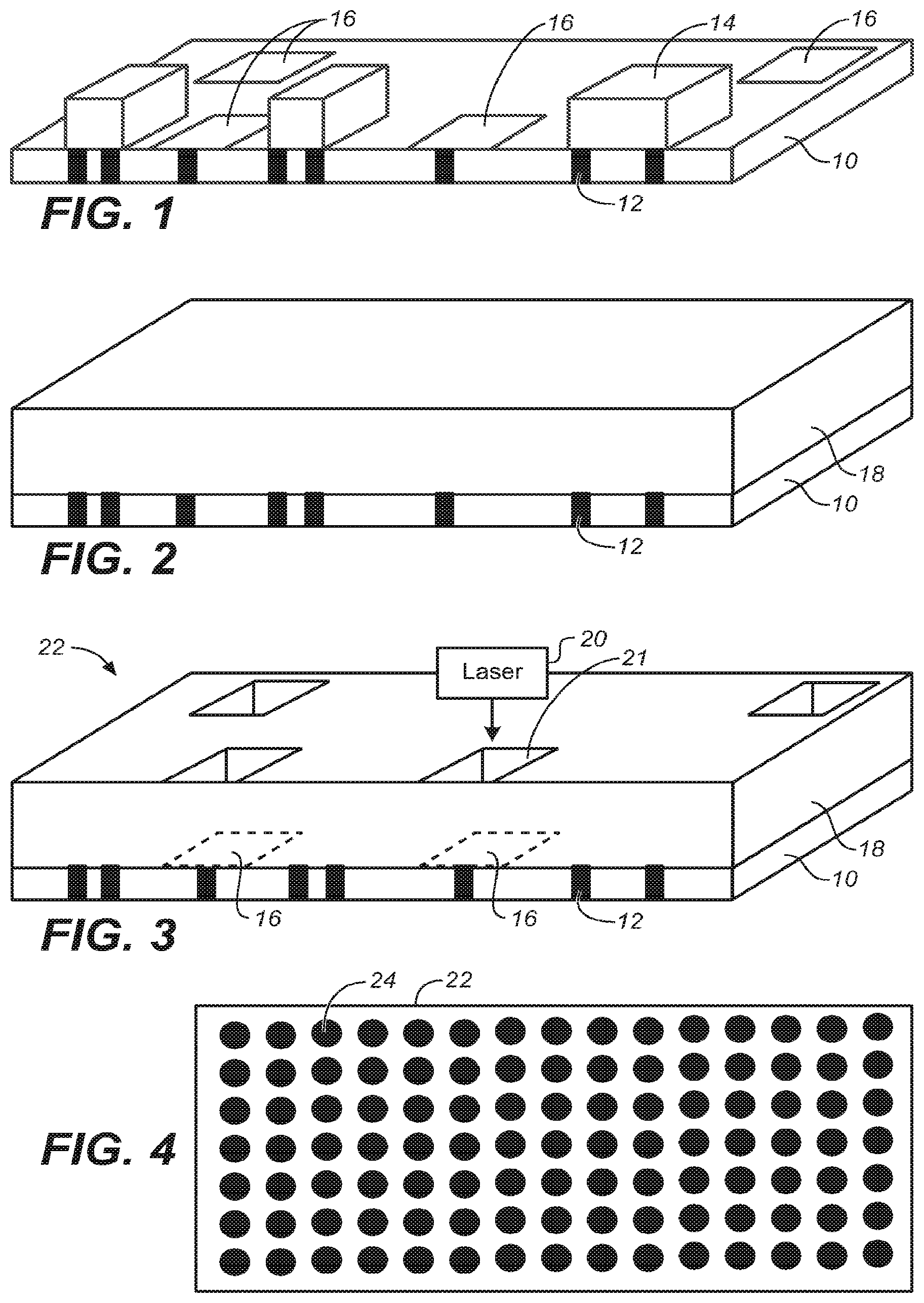
[0019] FIG. 1 is a cross-sectional perspective view of a substrate with circuitry mounted on the top of the substrate and conductive through-vias that electrically contact bottom pads of the substrate. Also shown are relatively large metal pads on the top of the substrate that are to be contacted by leads of an upper package.
[0020] FIG. 2 illustrates the substrate of FIG. 1 after a thermal plastic is molded over the top of the substrate to encapsulate the circuitry and provide a planar top surface.
[0021] FIG. 3 illustrates a programmed laser drilling holes in the thermal plastic to expose the pads on the substrate.
[0022] FIG. 4 illustrates the bottom of the package showing a ball grid array configuration for being soldered to a printed circuit board.
[0023] FIG. 5 illustrates one type of upper package whose metal posts are inserted through the holes in the bottom package to electrically contact the pads formed on the substrate.
[0024] FIG. 6 illustrates the upper package of FIG. 5 as well as a transparent bottom package.
[0025] FIG. 7 illustrates an alternative to FIG. 6 where excess solder, or other conductive material, is deposited in the holes and wick up the posts when melted for a robust electrical connection.
[0026] FIG. 8 illustrates a completed stacked package where the upper package uses staple-type leads around the perimeter of the upper package, and where the staple-type leads are inserted into laser drilled slots in the bottom package and electrically contact metal pads on the substrate in the bottom package.
[0027] FIG. 9 illustrates the stacked package of FIG. 8 with a transparent bottom package.
[0028] FIG. 10 illustrates multiple upper packages mounted over a single bottom package, where the tops of all the upper packages are co-planar.
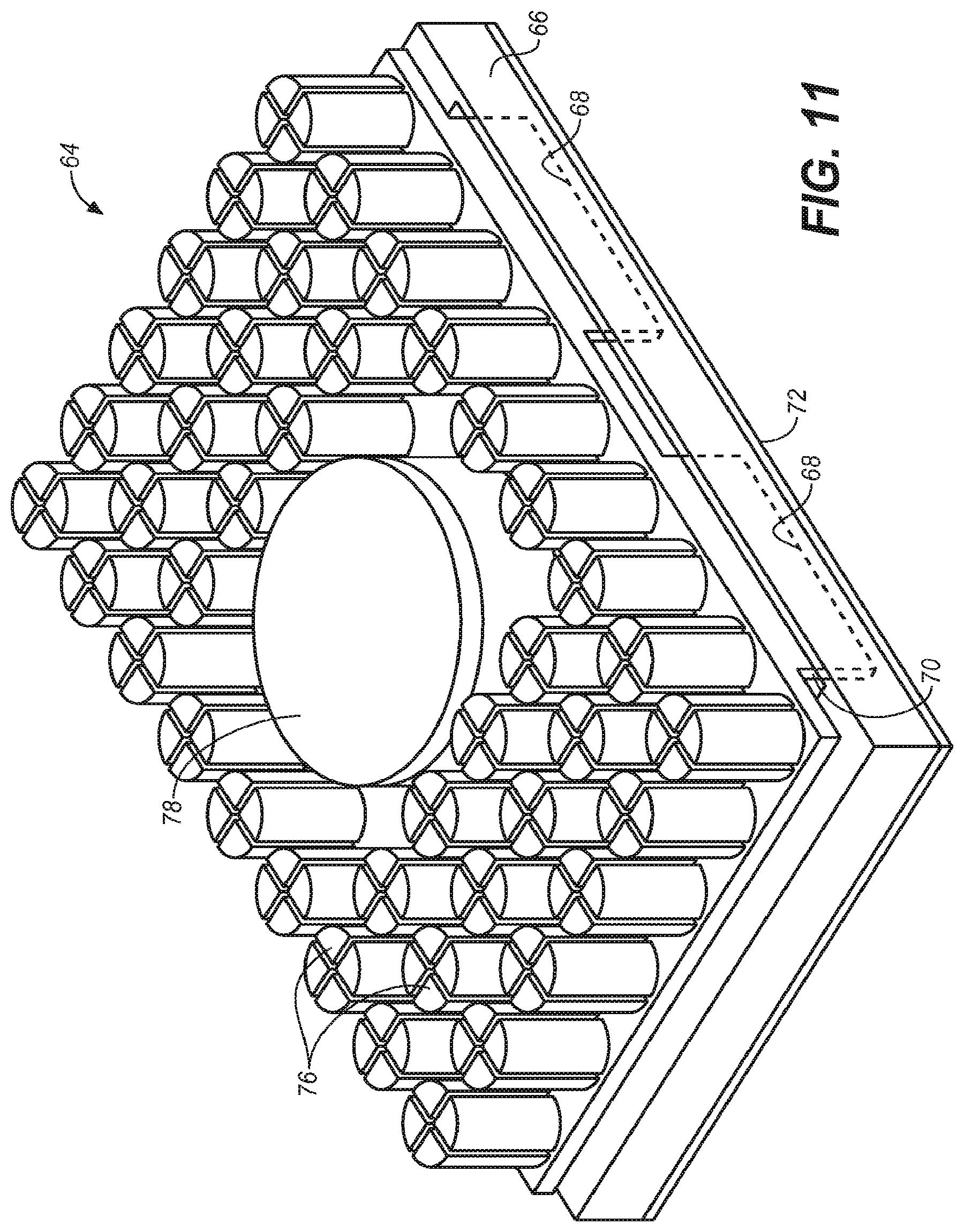
[0029] FIG. 11 illustrates a metal heat sink having tabs inserted through holes in the bottom package that are thermally connected to metal pads on the substrate of the bottom package.
DETAILED DESCRIPTION
[0030] Although the stacked package may be used for any type of circuitry, an example will be provided for a high power switching regulator having a stacked transformer or inductor. The regulator may provide an output current of up to 100 A to a load due to the particular design described.
[0031] FIG. 1 is a cross-sectional view of a starting substrate 10 for a bottom package. The substrate 10 may be a conventional printed circuit board material or a molded thermal plastic. In one embodiment, the substrate 10 is about 0.3 mm thick. The substrate 10 has conductive through-vias 12 that may be contacted by metal traces on the top the surface of the substrate 10 that interconnect circuit components 14. The components 14 may include integrated circuits and discrete components. The vias 12 terminate in bottom metal pads, such as for a ball grid array.
[0032] Relatively large top pads 16 are also shown, which align with leads of an upper package. Some of the vias 12 may terminate in the top pads 16. The pads 16 may be interconnected to other circuitry on the substrate 10. The vias 12 may be used for conducting heat from the upper package to a metal core printed circuit board. Some vias 12 may be connected together for a parallel conduction path.
[0033] In the example, the circuitry forms a switching transistor and control circuitry for a switching voltage regulator.
[0034] FIG. 2 illustrates a thermal plastic 18 molded over the substrate 10 to encapsulate the circuitry. The top of the plastic 18 is planar. The plastic 18 is a very good conductor of heat and is a dielectric.
[0035] In FIG. 3, a programmed laser 20 ablates holes 21 (of any shape) in the plastic 18 to expose the pads 16 on the substrate 10. In one embodiment, the pads 16 are formed to have a layer of solder for better wicking to metal leads of an upper package. The laser drilling automatically stops at the solder/pad surface and may clean the surface. The resulting structure is a bottom package 22 for the stacked package structure.
[0036] FIG. 4 illustrates a possible bottom surface of the bottom package 22 showing small metal pads 24 for a ball grid array.
[0037] A conductive material, such as solder, a solder paste, or a conductive epoxy is then dispensed into each of the holes 21 and will be used to electrically connect leads of an upper package to the pads 16 while not requiring the leads to directly abut the pads 16. This conductive material filling the gap between the leads and the pads 16 allows the upper package to be tilted, during a reflow step, to be precisely parallel to the bottom package 22 even if the leads are not planar.
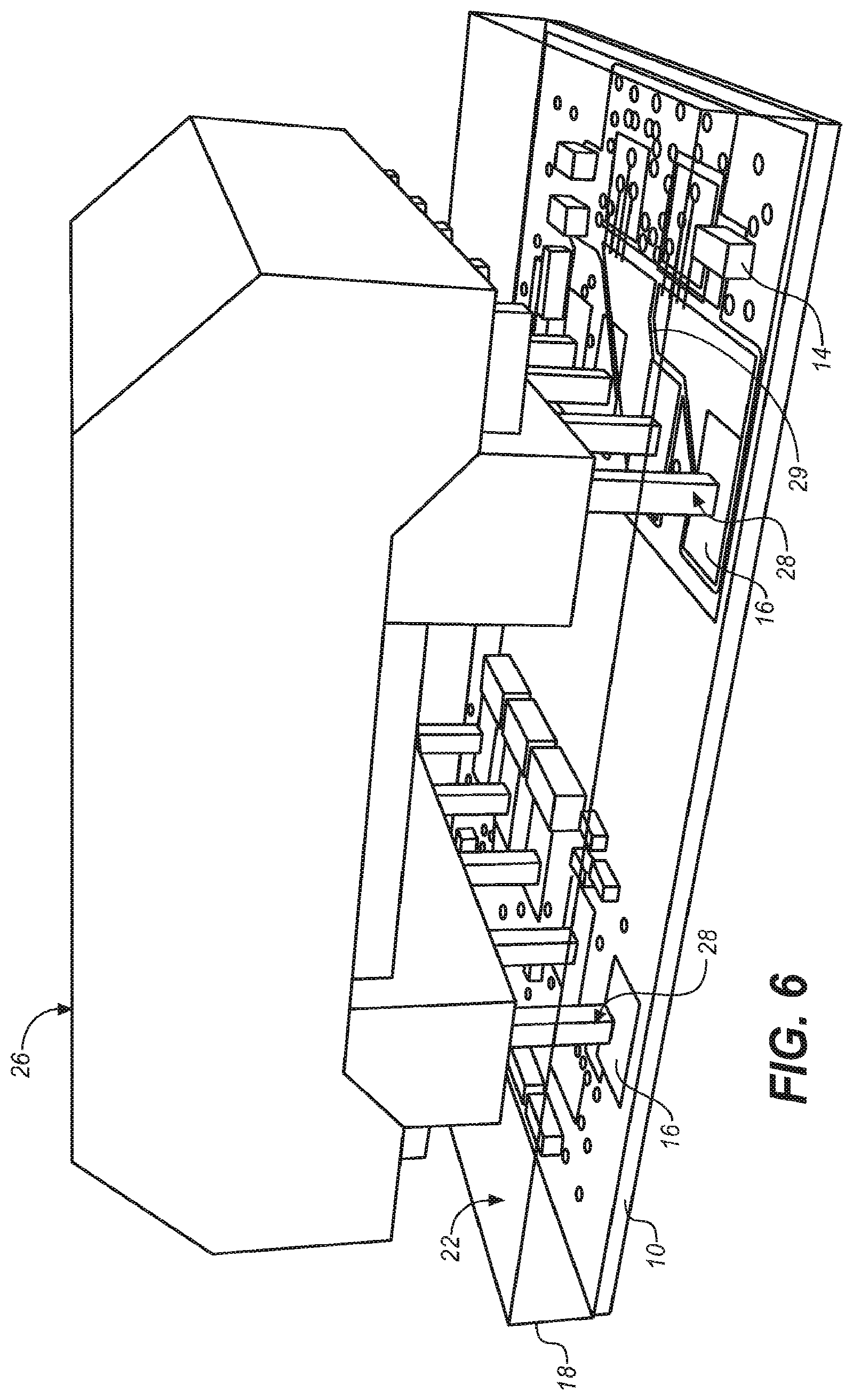
[0038] FIG. 5 illustrates an upper package 26 having leads formed as rectangular posts 28. The holes 21 in the bottom package 22 align with the pattern of the posts 28. The bottom surface of the upper package 26 does not need to contact the top surface of the bottom package 22, and the angle of the upper package 26 may be adjusted during reflow to achieve a precise alignment of the upper package 26 with the bottom package 22. In one embodiment, the upper package 26 contains a transformer.
[0039] FIG. 6 illustrates the structure of FIG. 5 but where the bottom package 22 is transparent. The ends of the posts 28 will not all abut the pads 16 on the substrate 10 if either the posts 28 or the pads 16 are not coplanar.
[0040] As shown in FIG. 7, to account for this lack of coplanarity, the holes in the bottom package 22 are partially filled with a conductive material 32, such as solder, a solder paste, or other conductive material, prior to inserting the posts 28 into the holes 21, that allows the upper package 26 to be positioned precisely parallel with the bottom package 22. The conductive material 32 may be dispensed with a needle or squeegeed into the holes 21. Thus, it is desirable to form the holes 21 significantly wider than the posts 28 so the conductive material 32 is not pushed out by the posts 28.
[0041] The bottom surface of the upper package 26 may optionally be affixed to the top of the bottom package 22 using a thermal epoxy to firmly set the position of the upper package 26 on the bottom package 22 after a reflow step. During reflow, the conductive material 32 will melt and wick to the posts 28 and pads 16 for a good electrical, thermal, and mechanical connection, while the upper package 26 is being precisely aligned with the bottom package 22 using an alignment tool. During the reflow, the heat also cures the thermal epoxy.
[0042] Conductive traces 29 on the substrate 10 are shown interconnecting circuit components 14 and the pads 16.
[0043] After the upper package 26 posts 28 are soldered to the pads 16, the structure may be turned over and solder balls placed on the bottom pads 24 (FIG. 4) of the bottom package 22 to form a ball grid array. A reflow step melts the solder over the pads 24. Such a reflow step does not affect the position of the upper package 26 if the upper package 26 is epoxied to the bottom package 22.
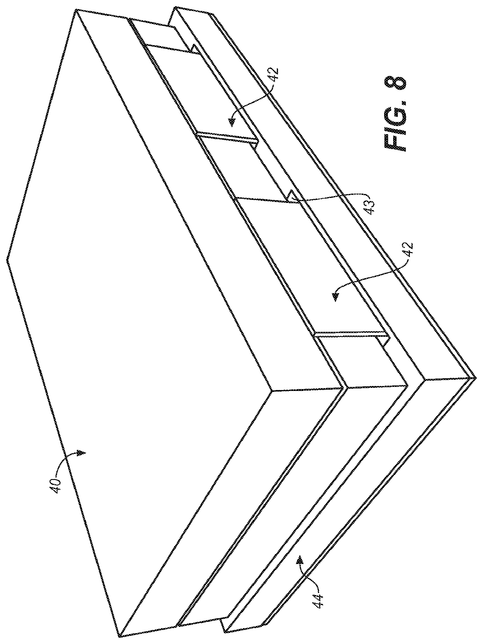
[0044] FIGS. 8-10 illustrate a different type of lead for the upper package 40 known as a staple lead 42. A staple lead is a thin and wide lead that is a good conductor of high currents and heat. It is particularly desirable when the upper package 40 is a high power inductor for a switching regulator. In one embodiment, the inductor is encased in a ferrite material which is highly thermally conductive.
[0045] The bottom package 44 may be identical to the bottom package of FIG. 3, except for the location and shape of the pads and the laser drilled holes 43.
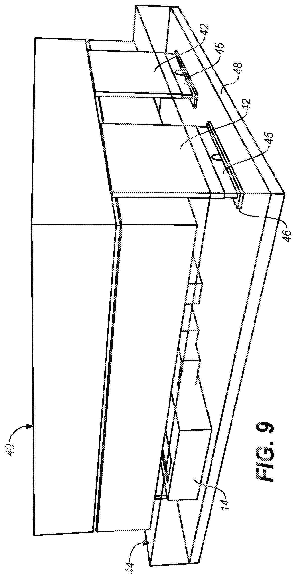
[0046] FIG. 9 shows the bottom package 44 as transparent and illustrates how the staple leads 42 extend through the laser drilled holes 43 (FIG. 8) in the bottom package 44 and may or may not abut the metal pads 46 formed on the substrate 48 of the bottom package 44. As previously described, after the holes 43 are formed, they are partially filled with a conductive material 45 that reflows and wicks to the pads 46 and the staple leads 42 for a good electrical, thermal, and mechanical connection.
[0047] The bottom of the upper package 40 may be epoxied to the top of the bottom package 44, using a thermal epoxy, to manipulate its alignment during the reflow step. The epoxy cures during the reflow step.
[0048] FIG. 10 illustrates how multiple upper packages 50-53 may be mounted over a single bottom package 56. The upper packages 50-53 each have four staple leads 42 that are inserted into laser drilled holes 58 in the bottom package 56 and electrically contact pads formed on the substrate 60. The bottom surface may be a ball grid array. Any other type of terminal configuration may be used.
[0049] Importantly, the ability to align each upper package 50-53 with respect to the bottom package 56 and with each other during the reflow step enables the top surfaces of all the upper packages 50-53 to be precisely coplanar. Therefore, a single heat sink with a flat surface may be positioned over the upper packages 50-53 and contact all the top surfaces equally.
[0050] FIG. 11 illustrates a heat sink 64 mounted over a bottom package 66. The heat sink 64 may be formed of copper or other thermally conductive material. The heat sink 64 has robust tabs 68 that extend into holes 70 (slots) laser drilled into the molded plastic of the bottom package 66. There may be distributed tabs 68 along the bottom of the heat sink 64, or the tabs 68 may just be along two or more sides of the heat sink 64.
[0051] The substrate 72 of the bottom package 66 has robust metal pads, similar to the pads 46 shown in FIG. 9, that are thermally coupled to the tabs 68. In one embodiment, prior to the heat sink 64 being mounted, a solder paste, a conductive epoxy, sinterable material, or some other thermally conductive material partially fills the holes 70, and the heat sink tabs 68 are inserted into the holes 70. The thermally conductive material fills any gap between the tabs 68 and the pads. Upon reflow, the thermally conductive material flows and then hardens, resulting in a good thermal and mechanical attachment of the heat sink 64 to the bottom package 66. The bottom surface of the heat sink 64 may be thermally epoxied to the top surface of the bottom package 66 for additional thermal contact. The heat sink 64 may be precisely aligned with the bottom package 66 during the reflow step, even if the tabs 68 are not coplanar, since the tabs 68 do not directly abut the metal pads on the substrate 72.
[0052] The metal pads on the substrate 72 may be grounded. The pads may also extend through the substrate 72 to terminate in the bottom pads 24 shown in FIG. 4. Such bottom pads 24 may then thermally contact a metal layer in a metal-core printed circuit board for additional heat sinking.
[0053] The heat sink 64 itself contains novel features. An array of segmented metal columns 76 is machined using conventional techniques to provide a large surface area for air cooling. A larger center protrusion 78, with a flat top, is provided to allow a robot arm or suction to grip the protrusion 78 and precisely mount the heat sink 64 on the bottom package 66 in an automated machine pick-and-place step.
[0054] In other embodiments, the upper package or other upper component may provide frequency isolation and/or shielding against RF, IF, or other radiated signal.
[0055] Multiple package structures may be formed simultaneously, and the packages are then singulated, such as by sawing.
[0056] In another embodiment, more than two packages may be vertically stacked using the techniques described above, where each upper package has leads that extend into laser drilled holes formed in its underlying package.
[0057] The technique described enables any degree of magnetic field isolation between the upper and bottom packages by providing a ground shield between the packages, or by providing adequate separation between the relevant components.
[0058] Instead of laser-drilling the holes, the holes may be formed by any other suitable method, such as during the molding of the bottom package, or mechanical drilling, or chemical etching.
[0059] While particular embodiments of the present invention have been shown and described, it will be obvious to those skilled in the art that changes and modifications may be made without departing from this invention in its broader aspects and, therefore, the appended claims are to encompass within their scope all such changes and modifications that are within the true spirit and scope of this invention.
* * * * *
D00001
D00002
D00003
D00004
D00005
D00006
D00007
D00008
XML
uspto.report is an independent third-party trademark research tool that is not affiliated, endorsed, or sponsored by the United States Patent and Trademark Office (USPTO) or any other governmental organization. The information provided by uspto.report is based on publicly available data at the time of writing and is intended for informational purposes only.
While we strive to provide accurate and up-to-date information, we do not guarantee the accuracy, completeness, reliability, or suitability of the information displayed on this site. The use of this site is at your own risk. Any reliance you place on such information is therefore strictly at your own risk.
All official trademark data, including owner information, should be verified by visiting the official USPTO website at www.uspto.gov. This site is not intended to replace professional legal advice and should not be used as a substitute for consulting with a legal professional who is knowledgeable about trademark law.