Method Of Forming A Photoresist Underlayer And Structure Including Same
Zyulkov; Ivan ; et al.
U.S. patent application number 17/065925 was filed with the patent office on 2021-04-15 for method of forming a photoresist underlayer and structure including same. The applicant listed for this patent is ASM IP Holding B.V.. Invention is credited to David Kurt de Roest, Michael Eugene Givens, Tatiana Ivanova, Bokheon Kim, Zecheng Liu, Daniele Piumi, Perttu Sippola, Yoann Tomczak, Ivan Zyulkov.
| Application Number | 20210111025 17/065925 |
| Document ID | / |
| Family ID | 1000005219024 |
| Filed Date | 2021-04-15 |


View All Diagrams
| United States Patent Application | 20210111025 |
| Kind Code | A1 |
| Zyulkov; Ivan ; et al. | April 15, 2021 |
METHOD OF FORMING A PHOTORESIST UNDERLAYER AND STRUCTURE INCLUDING SAME
Abstract
Methods of forming structures including a photoresist underlayer and structures including the photoresist underlayer are disclosed. Exemplary methods include forming the photoresist underlayer that includes metal. Techniques for treating a surface of the photoresist underlayer and/or depositing an additional layer overlying the photoresist underlayer are also disclosed.
| Inventors: | Zyulkov; Ivan; (Brussels, BE) ; de Roest; David Kurt; (Kessel-Lo, BE) ; Tomczak; Yoann; (Leuven, BE) ; Givens; Michael Eugene; (Phoenix, AZ) ; Sippola; Perttu; (Helsinki, FI) ; Ivanova; Tatiana; (Espoo, FI) ; Liu; Zecheng; (Helsinki, FI) ; Kim; Bokheon; (San Jose, CA) ; Piumi; Daniele; (Etterbeek, BE) | ||||||||||
| Applicant: |
|
||||||||||
|---|---|---|---|---|---|---|---|---|---|---|---|
| Family ID: | 1000005219024 | ||||||||||
| Appl. No.: | 17/065925 | ||||||||||
| Filed: | October 8, 2020 |
Related U.S. Patent Documents
| Application Number | Filing Date | Patent Number | ||
|---|---|---|---|---|
| 62913262 | Oct 10, 2019 | |||
| 63060777 | Aug 4, 2020 | |||
| Current U.S. Class: | 1/1 |
| Current CPC Class: | H01L 21/0337 20130101; H01L 21/0332 20130101; H01L 21/0273 20130101 |
| International Class: | H01L 21/033 20060101 H01L021/033; H01L 21/027 20060101 H01L021/027 |
Claims
1. A method of forming a structure comprising a photoresist underlayer, the method comprising the steps of: providing a substrate; forming a photoresist underlayer overlying a surface of the substrate using a cyclic deposition process; wherein the photoresist underlayer comprises one or more of an oxide, a nitride, and an oxynitride of a metal; wherein the metal comprises one or more transition metals.
2. The method of claim 1, wherein the photoresist underlayer comprises the metal, oxygen, and carbon, and wherein a metal-containing precursor is provided to the reaction chamber during the step of forming a photoresist underlayer, wherein the metal-containing precursor is an alkoxide or alkylamide metal precursor.
3. The method according to claim 2 wherein the metal-containing precursor has a general formula M[R(C.sub.xH.sub.y).sub.n].sub.4, wherein M is selected from Ti, Ta, Hf, Zn, and Zr, wherein R is selected from OCH and N, wherein x is 1 or 2, wherein y is 3-6, and wherein n is 2 or 3.
4. The method according to claim 3 wherein M is Ti.
5. The method according to claim 4 wherein the metal-containing precursor is titanium(IV) isopropoxide.
6. The method of claim 3, wherein a carbon precursor is further provided to the reaction chamber during the step of forming a photoresist underlayer, wherein the carbon precursor comprises one or more of an organic a carboxylic acid anhydrate, toluene, diethylene glycol, triethylene glycol, acetaldehyde, and an organosilicon compound.
7. The method according to claim 3, wherein the photoresist underlayer is formed using a reactant selected from H.sub.2O, O.sub.3, and H.sub.2O.sub.2.
8. The method according to claim 1, wherein the photoresist underlayer is formed using a plasma ALD or a plasma-enhanced pulsed CVD method that employs a plasma selected from the list consisting of H.sub.2, H.sub.2/He, H.sub.2/Ar, Ar, and O.sub.2 plasmas
9. The method of claim 3, further comprising a surface treatment step.
10. The method of claim 9, wherein the surface treatment step comprises exposing the photoresist underlayer to one or more carbon-containing compounds selected from the group consisting of a carboxylic acid anhydrate, toluene, diethylene glycol, triethylene glycol, acetaldehyde, and organosilicon compounds, such as silane and siloxanes.
11. The method of claim 3, further comprising a step of forming a carbon-containing layer overlying the photoresist underlayer, the carbon-containing layer comprising silicon, oxygen, and carbon.
12. The method of claim 3, further comprising a step of forming a self-assembled layer overlying the photoresist underlayer, wherein the self-assembled layer is formed of a material selected from the group consisting of dimethylamino-trimethylsilane, hexamethyldisilazane, (3-bromopropyl)trimethoxysilane, (3-iodopropyl)trimethoxysilane, 3-(trimethoxysilyl)propyl acrylate, trimethoxyphenyl silane, trimethoxy (3,3,3-trifluoropropyl)silane, 1H,1H,2H,2H-perfluorooctyltriethoxysilane, and tichloro(phenyl)silane, and trimethoxy(1H,1H,2H,2H-heptadecafluorodecyl)silane.
13. The method according to claim 1 wherein forming the underlayer comprises forming a lower underlayer part and an upper underlayer part.
14. The method according to claim 13 wherein the lower underlayer part is formed using a metal halogenide precursor, or wherein the lower underlayer part is formed using a metal-containing precursor having a general formula M[R(C.sub.xH.sub.y).sub.n].sub.4, where M is selected from Ti, Ta, Hf, Zn, and Zr, wherein R is selected from OCH and N, wherein x is 1-2, wherein y is 3-6, and wherein n is 2-3; and, wherein the upper underlayer part is formed using a metal-containing precursor having a general formula M[R(C.sub.xH.sub.y).sub.n].sub.4, where M is selected from Ti, Ta, Hf, Zn, and Zr, wherein R is selected from OCH and N, wherein x is 1-2, wherein y is 3-6, and wherein n is 2-3.
15. The method according to claim 14 wherein the upper underlayer part is formed using plasma-enhanced ALD or plasma-enhanced chemical vapor deposition, wherein a noble gas is used as a plasma gas.
16. The method according to claim 3 further comprising a step of exposing the underlayer to a surface treatment, the surface treatment comprising a step of exposing the underlayer to an organosilicon compound selected from the list consisting of bis(tripropylsilyl)amine, bis(triethylsilyl)amine, bis(trimethylsilyl)amine, (dimethylamino)trimethylsilane, (diethylamino)trimethylsilane, (diethylamino)triethylsilane, and (dimethylamino)triethylsilane.
17. The method according to claim 13 wherein the lower underlayer part has a laminar structure comprising alternating silicon containing lamellae and metal containing lamellae, wherein forming the underlayer comprises executing a plurality of sub-cycles x and sub cycles y, wherein sub cycles x and sub cycles y are carried out alternatingly, wherein sub cycle x comprises exposing the substrate to a silicon precursor in a reaction chamber; purging excess silicon precursor from the reaction chamber; subjecting the substrate to a plasma; and purging excess reactive species from the reaction chamber; and, wherein sub cycle y comprises exposing the substrate to a metal precursor; purging excess metal precursor from the reaction chamber; exposing the substrate to a plasma; and, purging excess reactive species from the reaction chamber.
18. The method according to claim 13 wherein the lower underlayer part comprises a metal silicide, and wherein forming the lower underlayer part comprises executing a plurality of sub-cycles x and sub cycles y, wherein sub cycles x and sub cycles y are carried out alternatingly, wherein sub cycle x comprises exposing the substrate to a silicon precursor in a reaction chamber; purging excess silicon precursor from the reaction chamber; subjecting the substrate to a plasma; and purging excess reactive species from the reaction chamber; and, wherein sub cycle y comprises exposing the substrate to a metal precursor; purging excess metal precursor from the reaction chamber; exposing the substrate to a plasma; and, purging excess reactive species from the reaction chamber.
19. A system configured for executing a method according to claim 13, the system comprising a first reaction chamber and a second reaction chamber, wherein the first reaction chamber is configured for depositing a lower underlayer part, wherein the second reaction chamber is configured for depositing an upper underlayer part, wherein the first reaction chamber operates at a first operating temperature, wherein the second reaction chamber operates at a second operating temperature, wherein the first operating temperature is higher than the second operating temperature;.
20. The system according to claim 19 further comprising a third reaction chamber, wherein the third reaction chamber is configured for subjecting the underlayer to a thermal or a plasma-enhanced post treatment, and wherein the first reaction chamber, the second reaction chamber, and/or the third reaction chamber comprise a showerhead gas distribution assembly.
Description
CROSS-REFERENCE TO RELATED APPLICATIONS
[0001] This application claims priority to U.S. Provisional Patent Application Ser. No. 62/913,262 filed Oct. 10, 2019, titled "METHOD OF FORMING A PHOTORESIST UNDERLAYER AND STRUCTURE INCLUDING SAME," and U.S. Provisional Patent Application Ser. No. 63/060,777 filed Aug. 4, 2020, titled METHOD OF FORMING A PHOTORESIST UNDERLAYER AND STRUCTURE INCLUDING SAME, the disclosures of which are hereby incorporated by reference in their entirety.
FIELD OF INVENTION
[0002] The present disclosure generally relates to structures and to methods of forming structures. More particularly, the disclosure relates to structures including or formed using a photoresist underlayer and to methods of forming such structures.
BACKGROUND OF THE DISCLOSURE
[0003] During the manufacture of electronic devices, fine patterns of features can be formed on a surface of a substrate by patterning the surface of the substrate and etching material from the substrate surface using, for example, gas-phase etching processes. As a density of devices on a substrate increases, it becomes increasingly desirable to form features with smaller dimensions.
[0004] Photoresist is often used to pattern a surface of a substrate prior to etching. A pattern can be formed in the photoresist, by applying a layer of photoresist to a surface of the substrate, masking the surface of the photoresist, exposing the unmasked portions of the photoresist to radiation, such as ultraviolet light, and removing a portion (e.g., the unmasked or masked portion) of the photoresist, while leaving a portion of the photoresist on the substrate surface.
[0005] Recently, techniques have been developed to use extreme ultraviolet (EUV) wavelengths to develop patterns having relatively small pattern features (e.g., 10 nm or less). To form features on a substrate using EUV, a photoresist underlayer of spin-on glass (SOG) is typically deposited onto a surface of a substrate, and then an EUV photoresist layer is deposited overlying the SOG underlayer. The underlayer generally has a thickness of about 10 nm or more.
[0006] As device feature sizes decrease, the underlayer may be desirably thinner to, for example, allow formation of etched features having desired pitch resolution and/or aspect ratios. Unfortunately, it can be difficult to deposit SOG at a thickness of less than 10 nm. Further, a within substrate and substrate-to-substrate thickness non-uniformity of deposited SOG can be undesirably high, particularly as a target thickness of the SOC layer is reduced.
[0007] Another challenge encountered when attempting to increase the resolution of lithographical patterning techniques, especially techniques employing EUV photoresist, is related to the EUV photoresist profile after the resist is exposed and developed. After the exposure and development resist profile might look tapered. In case the width of the resist lines at the bottom of the structure is lower than the width of the lines at the top of the structures, lines may collapse. In case the trend is the opposite--lines are wider at the bottom than at the top--lines will be very stable on the underlaying surface, but the pattern transfer will be difficult, and it would result in higher line edge roughness/line width roughness values.
[0008] Another challenge encountered when attempting to increase the resolution of lithographical patterning techniques, especially techniques involving EUV photoresist, is related to induced porosity in underlaying layers, e.g. carbon hardmasks, when exposed to depositions and/or surface treatments involving the use of a plasma.
[0009] For at least these reasons, improved structures including a photoresist underlayer, such as an underlayer suitable for use with EUV, and methods of forming such structures are desired. Particularly desired are underlayers having good adhesion to EUV resist, having a thickness of less than about 5 nm, and being resistant to etch chemistries which may be used for etching underlying layers.
[0010] The following prior art documents are made of record: Dufond, Maxime E., et al. "Quantifying the Extent of Ligand Incorporation and the Effect on Properties of TiO2 Thin Films Grown by Atomic Layer Deposition Using an Alkoxide or an Alkylamide." Chemistry of Materials 32.4 (2020): 1393-1407.
[0011] Any discussion of problems and solutions set forth in this section has been included in this disclosure solely for the purpose of providing a context for the present disclosure and should not be taken as an admission that any or all of the discussion was known at the time the invention was made.
SUMMARY OF THE DISCLOSURE
[0012] Various embodiments of the present disclosure relate to structures including improved photoresist underlayers (sometimes referred to as adhesion layers) and to methods of forming the layers and structures. While the ways in which various embodiments of the present disclosure address drawbacks of prior methods and structures are discussed in more detail below, in general, various embodiments of the disclosure provide structures that can include a relatively thin, uniform photoresist underlayer with desired properties, such as desired etch selectivity, pattern quality, and/or stability. Further, exemplary photoresist underlayers can be formed using a cyclical process, such as atomic layer deposition, which allows for precise control of a thickness of the photoresist underlayer--both on a surface of a substrate and from substrate to substrate. In addition, as set forth in more detail below, precursors, deposition conditions, post-deposition treatment parameters, and the like, can be adjusted or selected to form photoresist underlayers with desired surface energy to promote desired adhesion between the photoresist underlayers and overlying photoresist.
[0013] In accordance with exemplary embodiments of the disclosure, a method of forming a structure includes providing a substrate, forming a photoresist underlayer overlying a surface of the substrate, and forming a layer of photoresist overlying the photoresist underlayer. The photoresist underlayer can include a metal, such as a transition metal. For example, the photoresist underlayer can be or include one or more of a metal oxide, a metal nitride, and a metal oxynitride. The photoresist underlayer can be formed using one or more of plasma-enhanced cyclic (e.g., atomic layer) deposition process and thermal cyclic deposition process. By way of examples, the cyclic deposition process can include a step of providing one or more metal precursors to a reaction chamber, a step of providing one or more of an oxidant and a nitriding agent to the reaction chamber, and in some cases, a step of providing one or more carbon precursors to the reaction chamber. The photoresist underlayer can have a thickness of less than 10 nm or less than 5 nm. The photoresist layer can be or include positive or negative tone extreme ultraviolet (EUV) lithography photoresist.
[0014] In accordance with exemplary aspects of the disclosure, the photoresist underlayer includes carbon. For example, the photoresist underlayer can include greater than 0.18 g/cm.sup.3, or greater than 5 at % or about 5 at % to about 30 at % carbon. In some cases, a concentration of carbon in the photoresist underlayer can vary with a height of the photoresist underlayer--e.g., a concentration of carbon near a top surface of the photoresist underlayer (e.g., in the top 1-2 nm) may be greater than the concentration of carbon in the lower or bulk of the photoresist underlayer. In these cases, a concentration of carbon in the top surface of the photoresist underlayer can be greater than 10 at % or about 10 at % to about 50 at % carbon.
[0015] In accordance with exemplary aspects of embodiments of the disclosure, the photoresist underlayer can be selected and/or formulated to have desired properties--e.g., desired surface energy properties to, for example, promote desired adhesion between the photoresist underlayer and an overlying photoresist layer. For example, as set forth in more detail below, various precursors, process conditions, treatments, and/or coatings can be employed to obtain desired photoresist underlayer surface energy properties. Exemplary values of a polar part of surface energy of the photoresist underlayer are between about 5 mN/m to about 25 mN/m or about 20 mN/m to about 40 mN/m. Exemplary values of a dispersive part of surface energy of the photoresist underlayer are between 10 mN/m to about 30 mN/m, or 5 mN/m to about 25 mN/m, or 20 mN/m to about 40 mN/m.
[0016] In accordance with some aspects of the disclosure, methods can include a step of forming a carbon-containing layer overlying the photoresist underlayer. The carbon-containing layer can be used to obtain a desired surface energy or can be treated to obtain a desired surface energy. Exemplary carbon-containing layers can include silicon, oxygen, and carbon. Additionally or alternatively, the carbon-containing layer can include amorphous carbon.
[0017] Exemplary methods can additionally or alternatively include a step of treating a surface, such as a surface of the photoresist underlayer. Exemplary treatments for modifying a surface energy of a photoresist underlayer include exposing a surface of the photoresist underlayer to one or more carbon-containing agents. Exemplary carbon-containing agents can include a chemical formula that includes C, O, and optionally N. By way of particular examples, the carbon-containing agents can be selected from the group consisting of one or more of an acid anhydrate (e.g., an acetic anhydrate), toluene, diethylene glycol, triethylene glycol, acetaldehyde, silanes, and siloxanes. Forming CH.sub.3-termineted molecules on a surface using a carbon-containing agent can lower the polar part of the surface energy to near zero, but may not appreciably change the dispersive part of the surface energy. Additionally or alternatively, a surface of the photoresist underlayer or a carbon-containing layer thereon can be treated with a fluorine containing precursor, such as perfluorodecyltrimethoxysilane--e.g., to lower a polar part and to decrease the dispersive part of the surface energy of the photoresist underlayer. Surfaces can also be treated with surface functionalizing agents, such as salinization agents, such as silanes and siloxanes. Further examples of suitable surface treatments/carbon-containing layers include self-assembled layers--e.g., monolayers. The self-assembled layers can be formed using precursors comprising one or more of silicon and carbon, such as silanes, siloxanes, fluorinated silanes and/or fluorinated siloxanes.
[0018] In accordance with additional exemplary embodiments of the disclosure, a structure that includes a photoresist underlayer is provided. The photoresist underlayer can be formed using a method as described herein. The photoresist underlayer can include, for example, a layer comprising a metal, such as one or more of a metal oxide, a metal nitride, and a metal oxynitride. Exemplary structures can include one or more carbon-containing layers, such an amorphous carbon and/or a SiOC layer, as described herein. A photoresist underlayer can be treated or functionalized using techniques described herein. The photoresist underlayer, either alone or with a carbon layer and/or treatment, can have surface energy properties as described herein. Exemplary structures can also include a layer of photoresist, such as negative tone or positive tone EUV photoresist.
[0019] Further described is a method of forming a structure comprising a photoresist underlayer, the method comprising the steps of: providing a substrate; forming a photoresist underlayer overlying a surface of the substrate; wherein the photoresist underlayer comprises a metal.
[0020] In some embodiments, the photoresist underlayer comprises one or more of a metal oxide, a metal nitride, and a metal oxynitride.
[0021] In some embodiments, the metal comprises one or more transition metals.
[0022] In some embodiments, a value of a polar part of surface energy of the photoresist underlayer is between about 5 mN/m to about 25 mN/m, or about 20 mN/m to about 40 mN/m.
[0023] In some embodiments, a value of a dispersive part of surface energy of the photoresist underlayer is between about 10 mN/m to about 30 mN/m, or about 5 mN/m to about 25 mN/m, or about 20 mN/m to about 40 mN/m.
[0024] In some embodiments, the photoresist underlayer further comprises greater than 0.18 g/cm3 or 5% atomic percent carbon.
[0025] In some embodiments, the photoresist underlayer is formed using a cyclic deposition process.
[0026] In some embodiments, the photoresist underlayer is formed using an atomic layer deposition process.
[0027] In some embodiments the photoresist underlayer is formed using a cyclic chemical vapor deposition process.
[0028] In some embodiments, a carbon precursor is provided to the reaction chamber during the step of forming a photoresist underlayer.
[0029] In some embodiments, a chemical formula of the carbon precursor comprises C and O.
[0030] In some embodiments, the carbon precursor comprises one or more of an organic compound, a carboxylic acid anhydrate, toluene, diethylene glycol, triethylene glycol, acetaldehyde, and organosilicon compounds, such as silane and siloxanes.
[0031] In some embodiments, the organosilicon compound is selected from the group consisting of (n,n-dimethylamino)trimethylsilane, trimethoxy(octadecyl)silane, trimethoxyphenylsilane, trichloro(3,3,3-trifluoropropyl)silane and hexamethyldisilazane.
[0032] In some embodiments, the photoresist underlayer comprises a metal, oxygen, and carbon, and a metal-containing precursor is provided to the reaction chamber during the step of forming a photoresist underlayer, wherein the metal-containing precursor is an alkoxide or alkylamide metal precursor.
[0033] In some embodiments, the metal-containing precursor has a general formula M[R(C.sub.xH.sub.y).sub.n].sub.4, where M is selected from Ti, Ta, Hf, Zn, and Zr; and R is selected from OCH and N, wherein x is 1-2, wherein y is 3-6, and wherein n is 2-3.
[0034] In some embodiments, M is Ti.
[0035] In some embodiments, the metal-containing precursor is titanium(IV) isopropoxide.
[0036] In some embodiments, the photoresist underlayer comprises Hf, and the photoresist underlayer is deposited using a precursor selected from tetrakis(ethylmethylamido)hafnium, dimethylbis(cyclopentadienyl)hafnium, and Hafnium(IV) tert-butoxide.
[0037] In some embodiments, the photoresist underlayer comprises Ta, and the photoresist underlayer is deposited using a precursor selected from pentakis(dimethylamino)tantalum, tantalum(V)ethoxide, tris(diethylamido)(tert-butylimido)tantalum, tris(ethylmethylamido)(tert-butylimido)tantalum, tantalum tetraethoxy dimethylaminoethoxide, and tert-butylimidotris(diethylamido)tantalum.
[0038] In some embodiments, the photoresist underlayer is formed using a thermal ALD or a thermal CVD method, and using a reactant selected from H.sub.2O, O.sub.3, and H.sub.2O.sub.2.
[0039] In some embodiments, the reactant comprises H.sub.2O and O.sub.3.
[0040] In some embodiments, the photoresist underlayer is formed using a plasma ALD or a plasma-enhanced pulsed CVD method that employs a plasma selected from the list consisting of Hz, Hz/He, Hz/Ar, Ar, and O.sub.2 plasmas.
[0041] In some embodiments, the method further comprises a surface treatment step.
[0042] In some embodiments, the surface treatment step comprises exposing the photoresist underlayer to one or more carbon-containing compounds.
[0043] In some embodiments, the one or more carbon-containing compounds are selected from the group consisting of a carboxylic acid anhydrate, toluene, diethylene glycol, triethylene glycol, acetaldehyde, and organosilicon compounds, such as silane and siloxanes.
[0044] In some embodiments, a thickness of the photoresist underlayer is less than 5 nm.
[0045] In some embodiments, the method further comprises a step of forming a carbon-containing layer overlying the photoresist underlayer.
[0046] In some embodiments, the carbon-containing layer comprises silicon, oxygen, and carbon.
[0047] In some embodiments, the carbon-containing layer comprises amorphous carbon.
[0048] In some embodiments, the method further comprises a step of forming a self-assembled layer overlying the photoresist underlayer.
[0049] In some embodiments, the self-assembled layer is formed of a material comprising one or more of silicon and carbon.
[0050] In some embodiments, the material comprises one or more Si--C bonds.
[0051] In some embodiments, the material is selected from the group comprising silanes and siloxanes.
[0052] In some embodiments, the material is selected from the group comprising fluorinated silanes and fluorinated siloxanes.
[0053] In some embodiments, the material is selected from the group comprising dimethylamino-trimethylsilane (DMA-TMS), hexamethyldisilazane (HMDS), (3-bromopropyl)trimethoxysilane, (3-iodopropyl)trimethoxysilane, 3-(trimethoxysilyl)propyl acrylate, trimethoxyphenyl silane, trimethoxy (3,3,3-trifluoropropyl)silane, 1H,1H,2H,2H-perfluorooctyltriethoxysilane, tichloro(phenyl)silane, and trimethoxy(1H,1H,2H,2H-heptadecafluorodecyl)silane (FTMS).
[0054] In some embodiments, the underlayer is formed at a temperature of at least 70.degree. C. to at most 300.degree. C.
[0055] In some embodiments, the underlayer is formed at a temperature of at least 70.degree. C. to at most 200.degree. C.
[0056] In some embodiments, the underlayer is formed at a temperature of at least 200.degree. C. to at most 300.degree. C.
[0057] In some embodiments, forming the underlayer comprises the formation of a lower underlayer part and an upper underlayer part.
[0058] In some embodiments, the lower underlayer part is formed using a metal halogenide precursor.
[0059] In some embodiments, the lower underlayer part is formed using a metal-containing precursor having a general formula M[R(C.sub.xH.sub.y).sub.n].sub.4, where M is selected from Ti, Ta, Hf, Zn, and Zr, wherein R is selected from OCH and N, wherein x is 1-2, wherein y is 3-6, and wherein n is 2-3.
[0060] In some embodiments, the upper underlayer part is formed using a metal-containing precursor having a general formula M[R(C.sub.xH.sub.y).sub.n].sub.4, where M is selected from Ti, Ta, Hf, Zn, and Zr, wherein R is selected from OCH and N, wherein x is 1-2, wherein y is 3-6, and wherein n is 2-3.
[0061] In some embodiments, the upper underlayer part is formed using plasma-enhanced ALD or plasma-enhanced chemical vapor deposition, wherein a noble gas is used as a plasma gas.
[0062] In some embodiments, the noble gas comprises Ar.
[0063] In some embodiments, the upper underlayer part comprises silicon, oxide, and carbon, the upper underlayer part has a thickness of from at least 0.1 nm to at most 2.0 nm, and the upper underlayer part is formed using an organosilicon precursor and an oxygen-containing reactant selected from O.sub.2, H.sub.2O, O.sub.2, and H.sub.2O.sub.2.
[0064] In some embodiments, the method comprises a step of exposing the underlayer to a surface treatment, the surface treatment comprising a step of exposing the underlayer to an organosilicon compound selected from the list consisting of bis(tripropylsilyl)amine, bis(triethylsilyl)amine, bis(trimethylsilyl)amine, (dimethylamino)trimethylsilane, (diethylamino)trimethylsilane, (diethylamino)triethylsilane, and (Dimethylamino)triethylsilane.
[0065] In some embodiments, the method further comprises a step of exposing the underlayer to a plasma.
[0066] In some embodiments, forming the underlayer comprises a plasma-enhanced atomic layer deposition (PEALD) process comprising one or more cycles, the cycles comprising: providing a substrate to a reaction chamber; exposing the substrate to one or more precursors; purging excess precursor from the reaction chamber; exposing the substrate to a noble gas plasma, the noble gas plasma comprising reactive species; and, purging excess reactive species from the reaction chamber.
[0067] In some embodiments, the lower underlayer part has a laminar structure comprising alternating silicon containing lamellae and metal containing lamellae.
[0068] In some embodiments, the lower underlayer part comprises a metal silicide.
[0069] In some embodiments, forming the underlayer comprises executing a plurality of sub-cycles x and sub cycles y, wherein sub cycles x and sub cycles y are carried out alternatingly, wherein sub cycle x comprises exposing the substrate to a silicon precursor in a reaction chamber; purging excess silicon precursor from the reaction chamber; subjecting the substrate to a plasma; and purging excess reactive species from the reaction chamber; and, wherein sub cycle y comprises exposing the substrate to a metal precursor; purging excess metal precursor from the reaction chamber; exposing the substrate to a plasma; and, purging excess reactive species from the reaction chamber.
[0070] In some embodiments, forming the lower underlayer part comprises executing a plurality of sub-cycles x and sub cycles y, and sub cycles x and sub cycles y are carried out alternatingly, and sub cycle x comprises exposing the substrate to a silicon precursor in a reaction chamber; purging excess silicon precursor from the reaction chamber; subjecting the substrate to a plasma; and purging excess reactive species from the reaction chamber; and, sub cycle y comprises exposing the substrate to a metal precursor; purging excess metal precursor from the reaction chamber; exposing the substrate to a plasma; and, purging excess reactive species from the reaction chamber.
[0071] In some embodiments sub cycle x) and/or sub cycle y) comprise the use of a H.sub.2 plasma.
[0072] In some embodiments, sub cycle x) and/or sub cycle y) comprise the use of a O.sub.2 plasma.
[0073] In some embodiments, sub cycle x) and/or sub cycle y) comprises the use of a noble gas plasma.
[0074] In some embodiments, sub cycle x) comprises the use of a O.sub.2 plasma, and sub cycle y) comprises the use of a H.sub.2 plasma.
[0075] In some embodiments, sub cycle x) comprises the use of a H.sub.2 plasma, and sub cycle y) comprises the use of a O.sub.2 plasma.
[0076] In some embodiments, sub cycle x) comprises the use of a noble gas plasma, and sub cycle y) comprises the use of a O.sub.2 plasma.
[0077] In some embodiments, sub cycle x) comprises the use of a O.sub.2 plasma, and sub cycle y) comprises the use of a noble gas plasma.
[0078] In some embodiments, sub cycle x) comprises the use of a noble gas plasma, and sub cycle y) comprises the use of a H.sub.2 plasma.
[0079] In some embodiments, sub cycle x) comprises the use of a H.sub.2 plasma, and sub cycle y) comprises the use of a noble gas plasma.
[0080] In some embodiments, sub cycle x) and/or sub cycle y) comprises the use of a N.sub.2 plasma, NH.sub.3 plasma, or N.sub.2/H.sub.2 plasma.
[0081] In some embodiments, the metal precursor has a general formula M[R(C.sub.xH.sub.y).sub.n].sub.4, where M is selected from Ti, Ta, Hf, Zn, and Zr, wherein R is selected from OCH and N, wherein x is 1-2, wherein y is 3-6, and wherein n is 2-3.
[0082] In some embodiments, the silicon precursor is selected from aminosilanes, alkylsilanes, alkoxysilane., and silicon halides.
[0083] In some embodiments, the method further comprises a step of forming a photoresist layer overlying the photoresist underlayer.
[0084] Further described herein is a structure formed according to a method as described herein.
[0085] Further described is a system configured for executing a method as described herein.
[0086] In some embodiments, the system comprises a first reaction chamber and a second reaction chamber, wherein both the first reaction chamber and the second reaction chamber are configured for depositing a lower underlayer part, wherein the second reaction chamber is configured for depositing an upper underlayer part, wherein the first reaction chamber operates at a first operating temperature, wherein the second reaction chamber operates at a second operating temperature, and wherein the first operating temperature is higher than the second operating temperature.
[0087] In some embodiments, the system comprises a third reaction chamber, wherein the third reaction chamber is configured for subjecting the underlayer to a thermal or a plasma-enhanced post treatment.
[0088] In some embodiments, the second reaction chamber is further configured for subjecting the underlayer to a thermal or a plasma-enhanced post treatment.
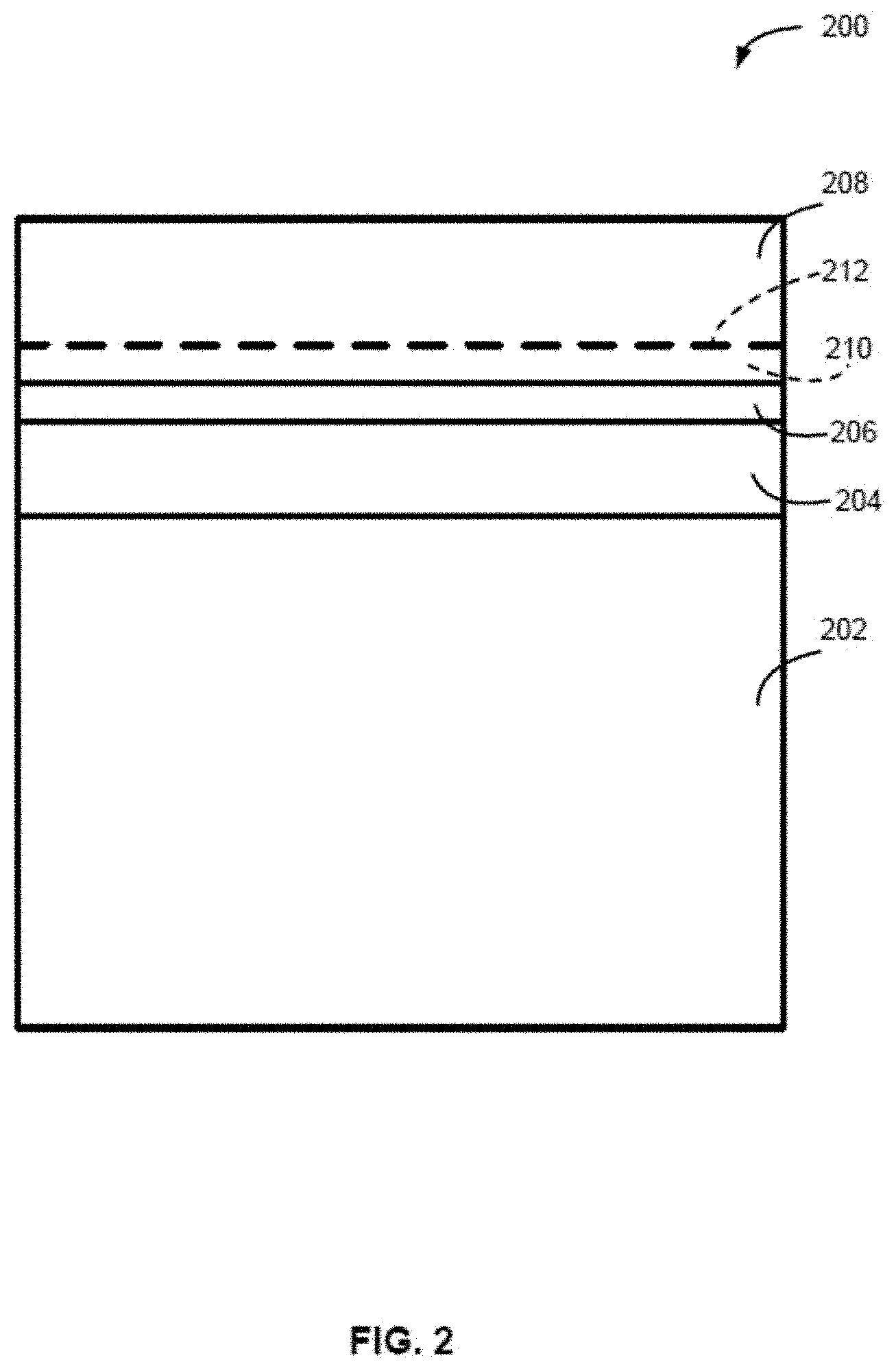
[0089] In some embodiments, the system comprises a reaction chamber comprising a showerhead gas distribution assembly.
[0090] In some embodiments, the first reaction chamber and/or the second reaction chamber comprise a showerhead gas distribution assembly.
[0091] In some embodiments, the third reaction chamber comprises a showerhead gas distribution assembly.
[0092] These and other embodiments will become readily apparent to those skilled in the art from the following detailed description of certain embodiments having reference to the attached figures; the invention not being limited to any particular embodiment(s) disclosed.
BRIEF DESCRIPTION OF THE DRAWING FIGURES
[0093] A more complete understanding of exemplary embodiments of the present disclosure can be derived by referring to the detailed description and claims when considered in connection with the following illustrative figures.
[0094] FIG. 1 illustrates a method of forming a structure in accordance with exemplary embodiments of the disclosure.
[0095] FIG. 2 illustrates a structure in accordance with exemplary embodiments of the disclosure.
[0096] FIG. 3 illustrates a structure in accordance with exemplary embodiments of the disclosure.
[0097] FIG. 4 illustrates another structure in accordance with exemplary embodiments of the disclosure.
[0098] FIG. 5 illustrates yet another structure in accordance with exemplary embodiments of the disclosure.
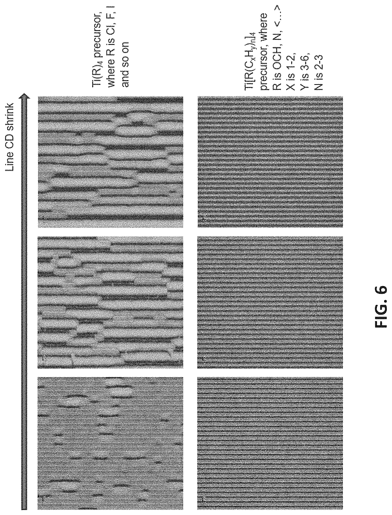
[0099] FIG. 6 shows experimental results that indicate that underlayers grown using a precursor of the general formula Ti[R(C.sub.xH.sub.y).sub.n].sub.4 allow obtaining a better resolution by means of EUV lithography compared to a case when underlayers are grown using a precursor of the general formula TiX.sub.4, with X being a halogen such as Cl, I, or F.
[0100] FIG. 7 shows a system (700) configured for executing a method as described herein.
[0101] FIG. 8 shows a structure (800) formed using specific embodiment of the present methods
[0102] FIG. 9 shows an exemplary process flow for the deposition of an underlayer.
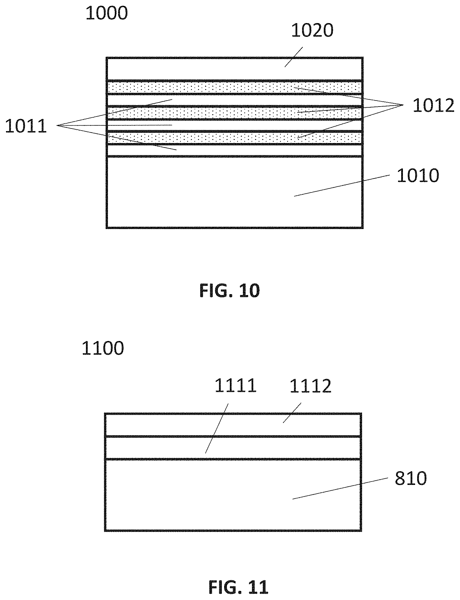
[0103] FIG. 10 shows an exemplary embodiment of a structure (1000) comprising a lower underlayer part and an upper underlayer part (1020).
[0104] FIG. 11 shows an embodiment of a structure (1100) comprising a lower underlayer part (1111) and an upper underlayer part (1112).
[0105] FIG. 12 shows a flow chart of exemplary embodiments of methods for forming an underlayer as described herein.
[0106] It will be appreciated that elements in the figures are illustrated for simplicity and clarity and have not necessarily been drawn to scale. For example, the dimensions of some of the elements in the figures may be exaggerated relative to other elements to help improve understanding of illustrated embodiments of the present disclosure.
DETAILED DESCRIPTION OF EXEMPLARY EMBODIMENTS
[0107] Although certain embodiments and examples are disclosed below, it will be understood that the invention extends beyond the specifically disclosed embodiments and/or uses thereof and obvious modifications and equivalents thereof. Thus, it is intended that the scope of the invention disclosed should not be limited by the particular disclosed embodiments described below.
[0108] The present disclosure generally relates to methods of forming structures that include a photoresist underlayer and to structures including a photoresist underlayer. As described in more detail below, exemplary methods can be used to form structures with photoresist underlayers that provide desired properties, such as desired thickness (e.g., less than 10 or less than 5 nm), relatively low surface roughness, good adhesion to the photoresist, desired etch selectivity, desired thickness uniformity--both within a substrate (e.g., a wafer) and between substrates, high pattern quality (low number of defects and high pattern fidelity), low line width roughness (LWR), stability during EUV lithography processing--e.g., during any post-exposure bake (PEB), photoresist development, reworking of the substrate, reasonable EUV sensitivity, and compatibility with integration (i.e., under the deposition conditions of underlayer, other layers underneath shall not be damaged--e.g., not too high deposition temperature). Further, as set forth below, exemplary embodiments of the disclosure can be used to tune surface properties, such as values of polar and dispersive parts surface energy of the photoresist underlayer--to, for example, promote adhesion between the photoresist underlayer and a layer of photoresist.
[0109] As used herein, the term "substrate" may refer to any underlying material or materials including and/or upon which one or more layers can be deposited. A substrate can include a bulk material, such as silicon (e.g., single-crystal silicon), other Group IV materials, such as germanium, or compound semiconductor materials, such as GaAs, and can include one or more layers overlying or underlying the bulk material. For example, a substrate can include a patterning stack of several layers overlying bulk material. The patterning stack can vary according to application. Further, the substrate can additionally or alternatively include various features, such as recesses, lines, and the like formed within or on at least a portion of a layer of the substrate.
[0110] In some embodiments, "film" refers to a layer extending in a direction perpendicular to a thickness direction. In some embodiments, "layer" refers to a material having a certain thickness formed on a surface or a synonym of film or a non-film structure. A film or layer may be constituted by a discrete single film or layer having certain characteristics or multiple films or layers, and a boundary between adjacent films or layers may or may not be clear and may or may not be established based on physical, chemical, and/or any other characteristics, formation processes or sequence, and/or functions or purposes of the adjacent films or layers. Further, a layer or film can be continuous or discontinuous.
[0111] In this disclosure, "gas" may include material that is a gas at normal temperature and pressure, a vaporized solid and/or a vaporized liquid, and may be constituted by a single gas or a mixture of gases, depending on the context. A gas other than the process gas, i.e., a gas introduced without passing through a gas distribution assembly, such as a showerhead, other gas distribution device, or the like, may be used for, e.g., sealing the reaction space, and may include a seal gas, such as a rare gas.
[0112] In some cases, such as in the context of deposition of material, the term "precursor" can refer to a compound that participates in the chemical reaction that produces another compound, and particularly to a compound that constitutes a film matrix or a main skeleton of a film, whereas the term "reactant" can refer to a compound, in some cases other than precursors, that activates a precursor, modifies a precursor, or catalyzes a reaction of a precursor; a reactant may provide an element (such as O, N, C) to a film matrix and become a part of the film matrix. In some cases, the terms precursor and reactant can be used interchangeably. The term "inert gas" refers to a gas that does not take part in a chemical reaction to an appreciable extent and/or a gas that excites a precursor when, for example, RF or microwave power is applied, but unlike a reactant, it may not become a part of a film matrix to an appreciable extent.
[0113] The term "cyclic deposition process" or "cyclical deposition process" may refer to the sequential introduction of precursors (and/or reactants) into a reaction chamber to deposit a layer over a substrate and includes processing techniques such as atomic layer deposition (ALD), cyclical chemical vapor deposition (cyclical CVD), and hybrid cyclical deposition processes that include an ALD component and a cyclical CVD component.
[0114] The term "atomic layer deposition" may refer to a vapor deposition process in which deposition cycles, typically a plurality of consecutive deposition cycles, are conducted in a process chamber. The term atomic layer deposition, as used herein, is also meant to include processes designated by related terms, such as chemical vapor atomic layer deposition, atomic layer epitaxy (ALE), molecular beam epitaxy (MBE), gas source MBE, or organometallic MBE, and chemical beam epitaxy when performed with alternating pulses of precursor(s)/reactive gas(es), and purge (e.g., inert carrier) gas(es).
[0115] Generally, for ALD processes, during each cycle, a precursor is introduced to a reaction chamber and is chemisorbed to a deposition surface (e.g., a substrate surface that can include a previously deposited material from a previous ALD cycle or other material), forming about a monolayer or sub-monolayer of material that does not readily react with additional precursor (i.e., a self-limiting reaction). Thereafter, in some cases, a reactant (e.g., another precursor or reaction gas) may subsequently be introduced into the process chamber for use in converting the chemisorbed precursor to the desired material on the deposition surface. The reactant can be capable of further reaction with the precursor. Purging steps can be utilized during one or more cycles, e.g., during each step of each cycle, to remove any excess precursor from the process chamber and/or remove any excess reactant and/or reaction byproducts from the reaction chamber.
[0116] In this disclosure, any two numbers of a variable can constitute a workable range of the variable, and any ranges indicated may include or exclude the endpoints. Additionally, any values of variables indicated (regardless of whether they are indicated with "about" or not) may refer to precise values or approximate values and include equivalents, and may refer to average, median, representative, majority, etc. in some embodiments. Further, in this disclosure, the terms "including," "constituted by" and "having" can refer independently to "typically or broadly comprising," "comprising," "consisting essentially of," or "consisting of" in some embodiments. In accordance with aspects of the disclosure, any defined meanings of terms do not necessarily exclude ordinary and customary meanings of the terms.
[0117] Turning now to the figures, FIG. 1 illustrates a method 100 in accordance with exemplary embodiments of the disclosure. Method 100 includes the steps of providing a substrate (step 102), forming a photoresist underlayer (step 104), and depositing a photoresist layer (step 106). Method 100 can also include one or more of forming a carbon-containing layer (step 108) and/or performing a surface treatment (step 110).
[0118] Step 102 includes providing a substrate, such as a substrate described herein. The substrate can include one or more layers, including one or more material layers, to be etched. By way of examples, the substrate can include a deposited oxide, a native oxide, or an amorphous carbon layer to be etched. The substrate can include several layers underlying the material layer(s) to be etched.
[0119] During step 104, a photoresist underlayer is formed on a surface of the substrate. In accordance with exemplary aspects of method 100, the photoresist underlayer is formed using a cyclical deposition process, such as an ALD process. The cyclical deposition process can include use of activated species (e.g., formed from one or more of precursor(s) reactant(s), or and/or inert gas(es)) that are formed using one or more of a direct plasma and a remote plasma. Alternatively, step 104 can include a thermal cyclical deposition process. Use of cyclical deposition processes may be desirable, because they allow for the formation of a photoresist underlayer with desired thickness--e.g., less than 10 nm or less than or about equal to 5 nm, with improved thickness uniformity--both within a substrate and from substrate-to-substrate. Using a plasma-enhanced process may be desirable, because plasma-enhanced processes allow for deposition of the photoresist underlayer material at relatively low temperatures.
[0120] In accordance with examples of the disclosure, a temperature within a reaction chamber during step 104 can be less than 500.degree. C., less than 400.degree. C., less than 300.degree. C. or between about 100.degree. C. and about 500.degree. C., or about 150.degree. C. and about 3000.degree. C. A pressure within the reaction chamber during step 104 can be about 1 Torr to about 100 Torr, about 3 Torr to about 50 Torr, or about 5 Torr to about 20 Torr.
[0121] In accordance with exemplary embodiments of the disclosure, step 104 includes forming or depositing one or more of a metal oxide, a metal nitride, and a metal oxynitride. In some cases, the photoresist underlayer can additionally include carbon. The carbon can be incorporated into the photoresist underlayer as the photoresist underlayer is deposited and/or a carbon treatment can be applied to a surface of the photoresist underlayer. Additionally or alternatively, a carbon-containing layer or other layer can be deposited onto a surface of the photoresist underlayer.
[0122] Carbon can be incorporated into a photoresist underlayer using one or more precursors that include carbon. For example, a cyclical process, such as an ALD process, can include (A) pulsing a first precursor comprising a metal into a reaction chamber, (B) pulsing a second precursor or reactant comprising an oxidant and/or nitriding agent into the reaction chamber, and (C) pulsing a carbon precursor into the reaction chamber. Each of the pulses can be separated by a purge step. Further, each pulsing step or a combination of pulsing steps (e.g., pulsing steps (A) and (B)) can be repeated a number of times prior to proceeding to the next step to tune an amount of carbon in the photoresist underlayer. For example, a range of ratios of (AB):C can be about 1:1 to about 1:10. Unless otherwise noted, steps (A), (B), and (C) can be performed in any order and various combinations of the steps can be repeated. However, in some cases, it may be desirable to initially form a metal oxide, nitride, or oxynitride by performing one or more cycles of steps (A) and (B) and then performing one or more cycles of step (C). Various combinations of steps (A), (B), and (C) can be performed to obtain a desired concentration grading throughout a thickness of the photoresist underlayer. In some cases, step (C) can be omitted.
[0123] In accordance with exemplary aspects of the disclosure, a first precursor comprising a metal can include a transition metal, such as hafnium, titanium, aluminum, zirconium, zinc and the like. The first precursor comprising a metal can also include carbon--e.g., one or more organic groups bonded directly or indirectly to a metal atom. By way of particular examples, the first precursor comprising a metal can include a metal halide or a metal organic compound, or an organometallic compound, such as one or more of tetrakis(dimethylamino)titanium (TDMAT), titanium isopropoxide (TTIP), titanium chloride (TiCl), tetrakis(ethylmethylamino)hafnium (TEMAHf), hafnium chloride (HfCl), trimethylaluminum (TMA), triethylaluminium (TEA), other metal halide, or other metal-containing compounds.
[0124] According to exemplary embodiments of the disclosure, the photoresist underlayer comprises a metal, oxygen, and carbon. Suitably, such photoresist underlayers may be formed by using a metal-containing precursor which is provided to the reaction chamber during the step of forming a photoresist underlayer. Suitably, the precursor comprises an alkoxide or alkylamide metal precursor. For example, the metal-containing precursor may have a general formula M[R(C.sub.xH.sub.y).sub.n].sub.4, where M is selected from Ti, Ta, Hf, Zn, and Zr, wherein R is selected from OCH and N, wherein x is 1-2, wherein y is 3-6, and wherein n is 2-3. In particular, titanium-containing precursors of the general formula Ti[R(C.sub.xH.sub.y).sub.n].sub.4 may be particularly suitable. Without the invention being bound by theory or any particular mode of operation, it is believed that precursor ligands may be incorporated in underlayers such as Titanium oxycarbide containing underlayers, which can improve resist adhesion. Thus, such underlayers do not necessarily require the presence of an adhesion or glue layer between the metal-containing layer and a subsequently deposited photoresist.
[0125] As shown in FIG. 6, using underlayers grown using a precursor of the general formula Ti[R(C.sub.xH.sub.y).sub.n].sub.4 allow obtaining a better resolution by means of EUV lithography compared to a case when underlayers are grown using a precursor of the general formula TiX.sub.4, with X being a halogen such as Cl, I, or F.
[0126] The oxidant and/or nitriding agent can include reactants that include one or more of oxygen and nitrogen. In some cases the reactant can include both nitrogen and oxygen. And, in some cases, the two or more oxidants and/or nitriding agents can be included in a single pulse. Exemplary oxidants and nitriding agents include oxygen (O.sub.2), water (H.sub.2O), ozone (O.sub.3), hydrogen peroxide (H.sub.2O.sub.2), NH.sub.3, diazene (N.sub.2H.sub.2), and the like.
[0127] The underlayers which are described herein may, for example, be deposited using a thermal ALD or a thermal CVD method. In this case, an oxidant may be selected as a reactant. For example, the oxidant may be selected from H.sub.2O, O.sub.3, and H.sub.2O.sub.2. Alternatively, the underlayers which are described herein may be deposited using plasma ALD or plasma pulsed-CVD. Suitable plasmas include H.sub.2, H.sub.2/He, H.sub.2/Ar, Ar or O.sub.2 plasmas. Both approaches may suitably provide for the deposition of thin (5 nm) TiO.sub.xC.sub.y with low non-uniformity.
[0128] The carbon precursor can include any suitable organic compound, such as compounds comprising carbon and oxygen. In some cases, the carbon precursor can also include nitrogen. The carbon precursor can be selected to react with, for example an --OH terminated surface of metal oxides and/or a --NH.sub.2 terminated surface of a metal nitride. Examples of suitable carbon precursors include one or more of organic compounds, such as acid anhydrate (e.g., an acetic anhydrate), toluene, diethylene glycol, triethylene glycol, acetaldehyde, and organosilicon compounds, such as silanes, and siloxanes. Exemplary organosilicon compounds include (n,n-dimethylamino)trimethylsilane, trimethoxy(octadecyl)silane, hexamethyldisilazane, trimethoxy(3,3,3-trifluoropropyl)silane, trimethoxyphenylsilane, trichloro(3,3,3-trifluoropropyl)silane and hexamethyldisilazane.
[0129] Generally, increasing a ratio and/or number of pulses of the carbon precursor can increase an amount of carbon in the photoresist underlayer. Higher carbon content in the photoresist underlayer can affect (e.g., lower) a polar part of the surface energy of the photoresist underlayer.
[0130] A thickness of photoresist underlayer formed during step 104 can be less than 10 nm or less than 5 nm. A carbon content of the photoresist underlayer can be greater than 3 at % carbon, greater than 5 at % carbon, greater than 10 at % carbon, or be about 5 to about 30 at % carbon. The carbon content can be substantially constant through a thickness of the photoresist underlayer. Or, the carbon content can be graded through a thickness of the photoresist underlayer. For example, step 104 can end with one or more steps of (C) pulsing a carbon precursor into the reaction chamber and/or include a higher ratio of step (C), relative to steps (A) and (B) near a top surface (e.g., top 1-2 nm) of the photoresist underlayer.
[0131] As illustrated in FIG. 1, method 100 can include a step 108 of forming a carbon-containing layer. The carbon-containing layer can be deposited in lieu of or in addition to incorporating carbon into the photoresist underlayer formed during step 104. The carbon-containing layer can be or include, for example, an amorphous carbon layer, a silicon carbon oxygen (SiOC) layer, or the like.
[0132] As used herein, unless stated otherwise, SiOC is not intended to limit, restrict, or define the bonding or chemical state, for example, the oxidation state of any of Si, O, C, and/or any other element in the film. Further, in some embodiments, SiOC thin films may comprise one or more elements in addition to Si, O, and/or C, such as H or N. In some embodiments, the SiOC films may comprise Si--C bonds and/or Si--O bonds. In some embodiments, the SiOC films may comprise Si--C bonds and Si--O bonds and may not comprise Si--N bonds. In some embodiments, the SiOC films may comprise Si--H bonds in addition to Si--C and/or Si--O bonds. In some embodiments, the SiOC films may comprise more Si--O bonds than Si--C bonds, for example, a ratio of Si--O bonds to Si--C bonds may be from about 1:10 to about 10:1. In some embodiments, the SiOC films may comprise from about 0% to about 50% carbon on an atomic basis. In some embodiments, the SiOC films may comprise from about 0.1% to about 40%, from about 0.5% to about 30%, from about 1% to about 30%, or from about 5% to about 20% carbon on an atomic basis. In some embodiments, the SiOC films may comprise from about 0% to about 70% oxygen on an atomic basis. In some embodiments, the SiOC films may comprise from about 10% to about 70%, from about 15% to about 50%, or from about 20% to about 40% oxygen on an atomic basis. In some embodiments, the SiOC films may comprise about 0% to about 50% silicon on an atomic basis. In some embodiments, the SiOC films may comprise from about 10% to about 50%, from about 15% to about 40%, or from about 20% to about 35% silicon on an atomic basis. In some embodiments, the SiOC films may comprise from about 0.1% to about 40%, from about 0.5% to about 30%, from about 1% to about 30%, or from about 5% to about 20% hydrogen on an atomic basis. In some embodiments, the SiOC films may not comprise nitrogen. In some other embodiments, the SiOC films may comprise from about 0% to about 40% nitrogen on an atomic basis (at %). By way of particular examples, SiOC films can be or include a layer comprising SiOCH, such as SiOCNH.
[0133] Step 108 can include a cyclical deposition process, such as an ALD process. For example, step 108 can include pulsing a carbon precursor to a reaction chamber, allowing the carbon precursor to react with a surface of a substrate, and purging any unreacted precursor and/or byproducts. Step 108 can also include providing one or more reactants, such as oxidants to the reaction chamber and purging. Step 108 can be a thermal process or a plasma-enhanced (direct and/or remote) process. Exemplary carbon precursor suitable for step 108 include any of the carbon precursors noted herein.
[0134] When the carbon-containing layer includes SiOC, step 108 can include providing a precursor comprising oxygen, silicon, hydrogen, and at least one organic group. For example, the precursor can include at least one silicon-oxygen bond. Additionally or alternatively, the precursor can include at least one silicon-R bond, wherein R is selected from, for example, one or more of the group consisting of alkyl (e.g., methyl group), alkenyl, alkynyl, aryl, alkoxy (e.g., --OCH.sub.3, --OCH.sub.2CH.sub.3), halogen and hydrogen. In some cases, the precursor includes at least two organic groups. By way of particular examples, the precursor can include one or more of di methyldimethoxysilane, di methoxytetramethyldisiloxa ne, octamethylcyclotetrasiloxane, tetramethylcyclotetrasiloxane (TMCTS), trimethylsilane (3MS), and diethoxymethylsilane (DEMS). A reactant can be selected from one or more of the group consisting of Ar, He, O.sub.2, CO.sub.2, CO, H.sub.2, N.sub.2O, H.sub.2O, and NH.sub.3. A temperature within a reaction space during the step of forming the photoresist underlayer can be, for example, between about 20.degree. C. and about 200.degree. C. or between about 150.degree. C. and about 350.degree. C. A pressure within the reaction chamber during step 108 can be about 1 Torr to about 100 Torr, about 3 Torr to about 50 Torr, or about 5 Torr to about 20 Torr.
[0135] When the carbon-containing layer includes amorphous carbon, step 108 can include deposition via thermal ALD, plasma-enhanced (PE) ALD, or PE CVD.
[0136] A thickness of the carbon-containing layer can be about 2 to about 3 nm or about 1 to about 2 nm. A concentration of carbon in the carbon-containing layer can range from about 50% to 100%, a concentration of oxygen in the carbon-containing layer can range from about 0% to about 30%, and a concentration of silicon in the carbon-containing layer can range from about 0% to about 30%.
[0137] As further illustrated in FIG. 1, method 100 can include surface treatment (or functionalization) step 110. Surface treatment step 110 can be performed in lieu of or in addition to either or both of incorporating carbon into the photoresist underlayer as the photoresist underlayer is formed and forming carbon-containing layer (step 108).
[0138] In some cases, step 110 includes treatment with a reactant, such as a halide gas, such as fluorine or chlorine to, for example, change a dispersive and/or polar part of the surface energy of the photoresist underlayer. The reactant can be thermally activated or activate using a plasma--e.g., a direct or remote plasma.
[0139] In some cases, step 110 can include treatment using one or more carbon-containing agents. Exemplary carbon-containing agents include any of the carbon precursors noted herein.
[0140] In accordance with further examples of the disclosure, silanization agents can be used to treat a substrate surface during step 110. Exemplary silanization agents can include silicon and one or more organic groups. For example, suitable silanization agents can include silicon bonded to one or more organic (e.g., methyl, oxymethyl, or the like) groups and/or include silicon bonded to nitrogen (e.g., a nitrogen atom bonded to one or more silicon atoms). The silanization agents can include silane compounds with a hydrolazible anchoring group, such as methoxy/ethoxy/Cl, F, or the like. By way of particular examples, step 110 can include exposing a surface of a substrate (e.g., a surface of a photoresist underlayer formed during step 104) to a silanization agent selected from the group consisting of dimethylamino-trimethylsilane (DMA-TMS), hexamethyldisilazane (HMDS), (3-bromopropyl)trimethoxysilane, (3-iodopropyl)trimethoxysilane, 3-(trimethoxysilyl)propyl acrylate, trimethoxyphenyl silane, trimethoxy (3,3,3-trifluoropropyl)silane, 1H,1H,2H,2H-perfluorooctyltriethoxysilane, tichloro(phenyl)silane, and trimethoxy(1H,1H,2H,2H-heptadecafluorodecyl)silane (FTMS).
[0141] Self-assembled (e.g., mono) layers can also be used to treat or functionalize a surface of a photoresist underlayer. In these cases, step 110 can include exposing a surface of a substrate (e.g., a surface of a photoresist underlayer formed during step 104) to a suitable precursor. Exemplary precursors suitable for forming self-assembly monolayers during step 110 include organic and organosilicon compounds, such as compounds including one or more of silicon and carbon (e.g., Si--C bonds), (e.g., silanes and siloxanes), such as compounds selected from the group consisting of perfluorodecyltrimethoxysilane (PFDTMS), tetramethoxysilane (TMOS), trimethoxy(octadecyl)silane, (TMODS), trimethoxy(3,3,3-trifluoropropyl)silane, triethoxyphenylsilane, trichloro(phenyl)silane, other silicon and carbon containing compounds described herein, and the like.
[0142] A temperature within a reaction chamber during steps 110 can be less than 500.degree. C., less than 400.degree. C., less than 300.degree. C. or between about 100.degree. C. and about 500.degree. C., or about 150 .degree. C. and about 300.degree. C. A pressure within the reaction chamber during step 110 can be about 1 Torr to about 100 Torr, about 3 Torr to about 50 Torr, or about 5 Torr to about 20 Torr, or from about 1 Torr to about 4 Torr, or from about 2 Torr to about 6 Torr.
[0143] During step 106, a layer of photoresist is deposited overlying the photoresist underlayer. The photoresist can be deposited using, for example, spin-on techniques. The photoresist layer can be or include positive or negative tone extreme ultraviolet (EUV) lithography photoresist.
[0144] FIG. 2 illustrates a structure 200 in accordance with exemplary embodiments of the disclosure. Structure 200 can be formed using, for example, method 100.
[0145] As illustrated, structure 200 includes a substrate 202, a material layer 204, a photoresist underlayer 206, and a photoresist layer 208. As illustrated, structure 200 can optionally include one or more of a carbon-containing layer 210 and/or a treated surface 212.
[0146] Substrate 202 can include a substrate as described above. By way of examples, substrate 202 can include a semiconductor substrate, such as a bulk material, such as silicon (e.g., single-crystal silicon), other Group IV semiconductor material, Group III-V semiconductor material, and/or Group II-VI semiconductor material and can include one or more layers (e.g., a patterning stack) overlying the bulk material. Further, as noted above, substrate 202 can include various topologies, such as recesses, lines, and the like formed within or on at least a portion of a layer of the substrate.
[0147] Material layer 204 can be patterned and etched using a photoresist underlayer and a layer of photoresist as described herein. Exemplary materials suitable for material layer 204 include, for example, oxides, such as native oxides or field oxides. Other exemplary material layer 204 materials include amorphous carbon, nitrides, other oxides, silicon, and add-on films (e.g. a self-assembled monolayer (e.g., hexamethyldisilazane (HMDS)).
[0148] Photoresist underlayer 206 can include a photoresist underlayer formed in accordance with a method described herein (e.g., method 100) and/or have properties as described herein. Exemplary photoresist underlayers include one or more of a metal oxide, a metal nitride, and a metal oxynitride. Photoresist underlayer 206 can, in some cases, include added carbon, as noted above. For example, photoresist underlayer 206 can have the carbon concentration and/or carbon concentration grading as noted herein.
[0149] A thickness of photoresist underlayer 206 can depend on a composition of material layer 204, a thickness of material layer 204, a type of photoresist, and the like. In accordance with examples of the disclosure, photoresist underlayer 206 has a thickness of less than 10 nm or less than or about 5 nm. If photoresist underlayer 206 is too thick, residual underlayer material may remain after an etch step. If photoresist underlayer 206 is too thin, photoresist underlayer 206 may not provide desired pattern transfer during an etch process. A surface of photoresist underlayer 206 (or a carbon-containing layer thereon) may or may not be treated with a treatment step (e.g., step 110), to provide desired surface terminations to, for example, promote adhesion with photoresist layer 208.
[0150] Photoresist underlayer 206 desirably exhibits good adhesion and other properties as described herein. To provide desired adhesion between photoresist layer 208 and photoresist underlayer 206, photoresist underlayer 206 may have or be tuned to have desired surface chemistry properties, e.g., quantified as surface energy, which is further categorized into a polar part of surface energy and a disperse part of surface energy. The polar part of surface energy and the disperse part of surface energy of photoresist underlayer 206 can be calculated by measuring a contact angle of a liquid, such as water or CH.sub.2I.sub.2, and using the Owens, Wendt, Rabel and Kaelble (OWRK) method to determine the polar part and the disperse part of the surface energy. The same properties can be measured and calculated for photoresist layer 208.
[0151] In accordance with various examples of the disclosure, a value of a polar part of surface energy of the photoresist underlayer is between about 5 mN/m to about 25 mN/m or about 20 mN/m to about 40 mN/m. In accordance with further examples, a value of a dispersive part of surface energy of the photoresist underlayer is between about 10 mN/m to about 30 mN/m, or about 5 mN/m to about 25 mN/m, or about 20 mN/m to about 40 mN/m. For example, when photoresist layer 208 comprises negative tone photoresist, a value of the polar part of surface energy of the photoresist underlayer can be between about 20 mN/m and about 40 mN/m and/or a dispersive part of surface energy of the photoresist underlayer can be between about 10 mN/m to about 30 mN/m or about 20 mN/m to about 40 mN/m. When photoresist layer 208 includes positive tone photoresist, a value of the polar part of surface energy of the photoresist underlayer can be between about 5 mN/m to about 25 mN/m and/or a value of the dispersive part of surface energy of the photoresist underlayer can be between about 10 mN/m to about 30 mN/m.
[0152] Carbon-containing layer 210 can include a carbon-containing layer, such as a carbon-containing layer described herein. Exemplary carbon-containing layers include amorphous carbon and/or SiOC layers. A thickness of layer 210 can be less than 5 nm or less than 2 nm. By way of examples, carbon-containing layer 210 can be about 1 to about 1.5 nm thick.
[0153] Treated (or functionalized) surface 212 can include any surface exposed to a treatment process, such as treatment step 110. By way of examples, treated surface can include a silanized surface and/or a surface comprising a self-assembled layer as described herein.
[0154] FIG. 3 illustrates a structure 300 in accordance with further exemplary embodiments of the disclosure. Structure 300 is similar to structure 200, except structure 300 does not include a carbon-containing layer or a photoresist layer.
[0155] Structure 300 includes a substrate 302, a material layer 304, and a photoresist underlayer 306. Substrate 302 can be the same or similar to substrate 202. Likewise, material layer 304 can be the same or similar to material layer 204. Photoresist underlayer 306 can be the same or similar to photoresist underlayer 206. However, in cases where structure 300 does not include a carbon-containing layer, photoresist underlayer 306 can include a relatively high amount of carbon--e.g., greater than 5 at % or about 5 at % to about 30 at % carbon. Structure 300 may be desirable, because structure 300 can be formed using relatively few process steps. Further, a concentration of carbon in photoresist underlayer 306 can be easily tuned--e.g., manipulating a ratio of carbon deposition steps relative to other deposition steps.
[0156] FIG. 4 illustrates a structure 400 in accordance with further exemplary embodiments of the disclosure. Structure 400 is similar to structure 200, except structure 400 does not include a photoresist layer and may, in some cases, not include a treated surface.
[0157] Structure 400 includes a substrate 402, a material layer 404, a photoresist underlayer 406, and a carbon-containing layer 408. Substrate 402 can be the same or similar to substrate 202. Likewise, material layer 404 can be the same or similar to material layer 204. Photoresist underlayer 406 can be the same or similar to photoresist underlayer 206. However, because structure 400 includes carbon-containing layer 408, photoresist underlayer 406 can include a relatively low amount of carbon--e.g., less than 5 at % or less than 10%. Carbon-containing layer 408 can include any carbon-containing layer described herein and can optionally be treated. Structure 400 may be desirable for some applications, because photoresist underlayer 406 can be or include a typical metal oxide, nitride, or oxynitride layer--e.g., without added carbon. In other words, additional steps to incorporate carbon into photoresist underlayer 406 may not be used.
[0158] FIG. 5 illustrates a structure 500 in accordance with further exemplary embodiments of the disclosure. Structure 500 is similar to structure 200, except structure 500 does not include a photoresist layer and does not include carbon-containing layer 210.
[0159] Structure 500 includes a substrate 502, a material layer 504, a photoresist underlayer 506, and a treated surface 508. Substrate 502 can be the same or similar to substrate 202. Material layer 504 can be the same or similar to material layer 204. Underlayer 506 can be the same or similar to photoresist underlayer 206. However, because structure 500 does not include a carbon-containing layer, underlayer 506 can include a relatively high amount of carbon--e.g., greater than 5 at % from about 5 at % to about 30 at %. Treated surface 508 can include material from one or more of the silanization agents and/or self-assembly precursors as described herein. Structure 500 may be desirable, because the surface treatment allows for very thin, self-limited material for treated surface 508. And, a wide variety of surface treatment agents can be used to form treated surface 508.
[0160] In some cases, a photoresist underlayer, or layer or treatment surface thereon, can be exposed to a post-deposition treatment step that includes formation of a plasma. In these cases, the plasma treatment step can include exposure of the photoresist underlayer to species activated using a direct and/or remote plasma. The plasma treatment step can include forming activated species from a gas including one or more of H.sub.2, O.sub.2, CO.sub.2, CO, N.sub.2O, NF.sub.3, and C.sub.xH.sub.yF.sub.z, where x>=1, y>=0, and z>=0. Such treatment can be used to, for example, further tune a dispersive and/or polar part of surface energy to desired values.
[0161] Although not illustrated, methods in accordance with the disclosure can include determining surface energy properties of a photoresist underlayer and/or a photoresist layer. For example, methods can include determining one or more of a disperse part and a polar part of surface energy of one or both of a photoresist layer and a photoresist underlayer. Methods can further include selecting photoresist underlayer material based on more of a disperse part and a polar part of surface energy of the photoresist layer and/or tuning based on more of a disperse part and a polar part of surface energy of the photoresist underlayer--e.g., using techniques described herein.
[0162] Further described, now referring to FIG. 7, is a system (700) configured for executing a method as described herein. The system comprises at least one reaction chamber which is configured for depositing an underlayer as described herein. The system may comprise a first reaction chamber (711) and a second reaction chamber (712) which may both be configured for depositing an underlayer as described herein, or a part thereof. Suitably, the first reaction chamber (711) operates at an operating temperature which is higher than the operating temperature of the second reaction chamber (712). Such a multi-chamber approach can be beneficial to maximize the etch resistance of metal-containing underlayers. In particular, the first reaction chamber (711) operating at a higher temperature can be used to deposit pure and dense metal oxide with high etch resistance, and the second reaction chamber (712) operating at a lower temperature may be suitably used to deposit metal oxide with good adhesion to the resist. Without the invention being bound to any particular theory or mode of operation, this is believed to be due to an increased incorporation of precursor ligands in the underlayer at lower deposition temperatures compared to higher deposition temperatures.
[0163] Optionally, the second reaction chamber (712) is further configured for subjecting the underlayer to a thermal or plasma-enhanced post-treatment. Alternatively, the system (700) may comprise a third reaction chamber (713) in which the thermal or plasma-enhanced post treatment may be carried out. The post treatment may, for example, employ a H.sub.2, H.sub.2/He, H.sub.2/Ar, Ar and/or O.sub.2 plasma.
[0164] In a specific example embodiment, the underlayer is deposited using a thermal ALD process. Titanium(IV) isopropoxide may be used as a precursor, and a mixture of H.sub.2O and O.sub.3 can be used as a co-reactant. Precursor and reactant are cyclically provided to a reaction chamber in alternating pulses. Suitable process temperatures include the range of 70.degree. C.-300.degree. C. A process temperature lower than 200.degree. C. advantageously improves adhesion to resist, which, without the invention being bound to theory or a particular mode of operation, is believed to be related to incorporation of precursor ligands and/or isopropanol by-products. A process temperature higher than 200.degree. C. advantageously provides increased etch resistance.
[0165] In a specific example embodiments, the underlayer is deposited using another thermal ALD process. Tetrakis(dimethylamido)titanium may be used as a precursor, and a mixture of H.sub.2O and O.sub.3 can be used as a co-reactant. Precursor and reactant are cyclically provided to a reaction chamber in alternating pulses. Suitable process temperatures include the range of 70.degree. C.-300.degree. C., and can result in a TiO.sub.2-containing film which has excellent properties. A process temperature lower than 200.degree. C. advantageously improves adhesion to resist, which, without the invention being bound to theory or a particular mode of operation, is believed to be related to incorporation of precursor ligands into the underlayer. A process temperature higher than 200.degree. advantageously provides increased etch resistance.
[0166] FIG. 8 shows a structure (800) formed using specific embodiment of the present methods which comprise the formation of a lower underlayer part (811) and an upper underlayer part (812) on a substrate (810). The substrate (810) may comprise a silicon wafer and optionally one or more patterned features and/or material layers. For example, the substrate (810) may comprise one or more of the layers underlying the photoresist underlayer, as shown in any one of the other figures contained herein.
[0167] In some embodiments, the lower underlayer part comprises a metal oxide, e.g. titanium oxide, and the upper underlayer part comprises carbon. In such embodiments, the lower underlayer part may have a thickness of, for example, from at least 1.0 to at most 5.0 nm, or from at least 2.0 nm to at most 3.0 nm. Also, the upper underlayer part may have a thickness of, for example, 0.1 nm to at most 2.0 nm, or from at least 0.5 nm to at most 1.0 nm.
[0168] The lower underlayer part may be formed using a metal halogenide precursor, e.g. a chloride, fluoride, bromide, or iodide of Hf, Ti, Ta, Zn, or Zr. The upper underlayer part may be formed using a metal-containing precursor having a general formula M[R(C.sub.xH.sub.y).sub.n].sub.4, where M is selected from Ti, Ta, Hf, Zn, and Zr, wherein R is selected from OCH and N, wherein x is 1-2, wherein y is 3-6, and wherein n is 2-3. Such a bi-layer underlayer structure may be particularly advantageous as it may combine a good etch resistance of the lower underlayer part with suitable surface properties provided by the upper underlayer part.
[0169] Additionally or alternatively, the upper underlayer part may comprise silicon, oxide, and carbon. In such embodiments, the upper underlayer part may have a thickness of, for example, from at least 0.1 nm to at most 2.0 nm, e.g. a thickness of 0.2 nm, 0.4 nm, 0.6 nm, 0.8 nm, 1.0 nm, or 1.5 nm. Such an underlayer may be formed, for example, by means of an ALD or CVD method, be it thermal or plasma-enhanced, using e.g. an organosilicon precursor and an oxygen reactant such as O.sub.2, H.sub.2O, O.sub.3, or H.sub.2O.sub.2.
[0170] The application of a noble gas plasma such as an Ar plasma for depositing the upper underlayer part be particularly advantageous. Without the invention being bound to any theory or particular mode of operation, this is believed to be caused by the presence of precursor ligands in the thusly formed layers, which can result in excellent adhesion properties.
[0171] An upper underlayer part may be formed using any one of plasma enhanced atomic layer deposition (PEALD) or pulsed plasma-enhanced chemical vapor deposition (pulses PECVD). In PEALD mode, precursors may be introduced in a reaction chamber containing a substrate, reacting with surface reactive sites and then chemisorbing on the substrate's surface. In a second step, excess precursor may be purged, be it partially or wholly, from the reaction chamber to avoid, minimize, or reduce CVD reactions. In a third step, the substrate may be exposed to a noble gas plasma (e.g. an Ar, He, Ne, Kr, or Xe plasma). In the fourth step, plasma power is switched-off for a pre-determined amount of time to purge away at least a part of the reactive species from the reaction chamber. This process may be repeated any number of times in order to obtain an upper underlayer part. Advantageously, such an upper underlayer part contains a metal-containing layer, e.g. a metal oxide, with a high carbon content, e.g. a carbon content of at least 10 atomic % to at most 70 atomic %, or at least 20 atomic % to at most 60 atomic %, or at least 30 atomic % to at most 50 atomic %, or of about 40 atomic %. The upper underlayer part may suitably serve as an adhesion layer or glue to a subsequently deposited photoresist layer.
[0172] Alternatively, in some embodiments, the upper underlayer part may be deposited using pulsed plasma enhanced chemical vapor deposition (pulsed PECVD). In an exemplary pulsed PECVD process for depositing an upper underlayer part, the substrate can be exposed to a noble gas plasma such as an Ar, He, Ne, Kr, or Xe plasma. Then, the substrate may be exposed to a metal precursor, while the plasma is kept on such that the precursor dissociates through the action of the plasma. Hence, carbon-containing metal layers, e.g. carbon containing metal oxide layers, can be formed on the substrate. Then, the supply of metal precursor is stopped. Optionally, the plasma is kept on for a pre-determined amount of time, e.g. 1.0 s to 60 s, or 2.0 s to 30 s, or 4.0 s to 15 s, or 6 s to 12 s. Without the invention being bound by theory or a particular mode of operation, it is believed that keeping the plasma on after the metal precursor flow has been stopped can advantageously modify the deposited layers's surface properties. By the aforementioned pulsed PECVD procedure, an upper underlayer part, e.g. a C-rich MOx adhesion layer, can be formed. When used with suitable EUV resists, it offers an improved process window against pattern collapse and a lower line edge roughness (LER) and line width roughness (LWR).
[0173] Note that suitable precursors for depositing the upper underlayer part, be it by means of pulsed PECVD or PEALD, include the metal precursors mentioned herein.
[0174] In some embodiments, the underlayer may be subjected to a surface treatment, e.g. a surface treatment that results in a surface termination. The surface treatment may be applied to both monolithic underlayers and to underlayers comprising a lower underlayer part and an upper underlayer part. Such a surface treatment may obviate the need for an upper underlayer part, or it may be used to treat the surface of an upper underlayer part.
[0175] Exemplary surface treatments using an organosilicon compound, such as a sylilamine. Exemplary organosilicon compounds include alkylaminosilylamines and/or alkylsilylamines such as bis(tripropylsilyl)a mine, bis(triethylsilyl)a mine, bis(trimethylsilyl)a mine, (dimethylamino)trimethylsilane, (diethylamino)trimethylsilane, (diethylamino)triethylsilane, and (Dimethylamino)triethylsilane. Additionally or alternatively, the surface treatment may comprise the use of fluoroalkyl-substituted silanes. Such fluorine-containing molecules can be used to lower the dispersive part of the surface energy of the underlayer. Additionally or alternatively, the surface treatment may comprise the use of a halogen-substituted silane and/or of an alkoxysilane such as a methoxysilane or an ethoxysilane. Additionally or alternatively, the surface treatment may comprise the use of a compound selected from the list consisting of (3-Bromopropyl)trimethoxysilane, (3-lodopropyl)trimethoxysilane, 3-(Trimethoxysilyl)propyl acrylate, Trimethoxyphenyl silane, Trimethoxy (3,3,3-trifluoropropyl)silane, and 1H,1H,2H,2H-Perfluorooctyltriethoxysilane.
[0176] Additionally or alternatively, the surface treatment may comprise subjecting the underlayer to a noble gas plasma, e.g. an Ar, He, Ne, Kr, or Xe plasma.
[0177] Such surface treatments allow suitably controlling the surface energy of the underlayer for improved photoresist adhesion.
[0178] Another possible surface treatment, which can be performed additionally or alternatively to the other surface treatments mentioned herein, includes subjecting the underlayer to a plasma such as a H plasma, an Ar/H plasma (i.e. a plasma comprising Ar and H), or a He/H plasma (i.e. a plasma comprising He and H). Subjecting the underlayer to such plasmas may result in the formation of CH.sub.3 and/or CH.sub.2 functional groups on the surface of the underlayer. Additionally or alternatively, the underlayer may be subjected to a halogen-containing plasma, such as a fluorine-containing plasma, such as a CF.sub.4 plasma, which may result in the formation of a Fluorine-terminated surface of the underlayer. Additionally or alternatively, the underlayer may be subjected to a chlorine-containing plasma, such as a Cl.sub.2 plasma, which may result in the formation of a chlorine-terminated surface of the underlayer.
[0179] Accordingly, the surface properties of the underlayer can be modified via i) deposition process (ALD/CVD) variation, and/or ii) a post-treatment, such as a plasma-based post treatment. Without the invention being bound by theory or any particular mode of operation, it is believed that the carbon concentration in the underlayer mainly affects the polarity of the surface, while termination with various elements (such as H, F, CI from a plasma) affects the dispersive component of the surface energy.
[0180] FIG. 9 shows an exemplary process flow for the deposition of an underlayer, a lower underlayer part, and/or an upper underlayer part by means of plasma-enhanced chemical vapor deposition. In the process, a substrate in a reaction chamber is exposed to one or more precursors. Then, excess precursor may be purged from the reaction chamber. Thereafter, the substrate may be subjected to a plasma. For example, in order to manufacture an upper underlayer part having good adhesion properties, a noble gas plasma may be used, e.g. a He, Ne, Ar, Kr plasma. After the plasma step, excess reactive species such as ions and radicals are suitably purged from the reaction chamber. The aforementioned steps form a cycle. These cycles can be repeated any number of times in order to deposit an underlayer or a part thereof having a desired thickness.
[0181] In an exemplary process, both the lower underlayer part and the upper underlayer part are formed using a plasma-enhanced chemical vapor deposition process. Exemplary, non-limiting process conditions for forming a lower underlayer part comprising titanium oxide include 0.4 s precursor feed time, 0.7 precursor purge time, precursor is carried by means of an Ar carrier gas, Ar carrier gas flow rate is 1 slm, additionally, a continuous flow of 1 slm argon as a plasma gas is provided, O.sub.2 is used as a reactant, O.sub.2 flow rate is 2 slm, plasma power is 100 W, plasma on time is 0.2 s, post-plasma purge time is 0.1 s, electrode gap is 12 mm, pressure is 400 Pa, susceptor temperature is 190.degree. C., and a lower underlayer part is formed in 31 cycles, yielding a thickness of 2.45 nm. Exemplary, non-limiting process conditions for forming an upper underlayer part comprising titanium oxide include: 0.4 s precursor feed time, 0.7 precursor purge time, precursor is carried by means of an Ar carrier gas, Ar carrier gas flow rate is 1 slm, additionally, a continuous flow of 1 slm argon as a plasma gas is provided, plasma power is 50 W, plasma on time is 2.2 s, post-plasma purge time is 0.1 s, electrode gap is 7.5 mm, pressure is 900 Pa, susceptor temperature is 190.degree. C., and the upper underlayer part is formed in 15 cycles, yielding a thickness of 0.5 nm. This example was given for underlayer formation on a substrate comprising a carbon hard mask. The combination of such a lower underlayer part and upper underlayer part allows obtaining an underlayer with a good etch resistance and good adhesion to photoresist. In addition, an upper underlayer part may protect layers covered by the underlayer, such as a carbon-containing layer, e.g. diamond-like carbon layers, amorphous carbon layers, or the like. Additionally, the application of an upper underlayer part may advantageously improve the density of the lower underlayer part.
[0182] It shall be understood that the lower underlayer part and/or the upper underlayer part may be deposited using deposition conditions which differ from the exemplary process conditions described above. For example, a lower underlayer part and/or an upper underlayer part may be deposited at a temperature of from at least 70.degree. C. to at most 300.degree. C. As another example, the lower underlayer part and/or the upper underlayer part may be deposited at a pressure of at least 100 Pa to at most 800 Pa, or at a pressure of at least 200 Pa to at most 600 Pa.
[0183] In some embodiments, the underlayer, be it monolithic or consisting of a lower underlayer part and an upper underlayer part, is deposited using thermal atomic layer deposition as opposed to plasma-enhanced atomic layer deposition. In such embodiments, it can be particularly advantageous to subject the underlayer to a plasma, e.g. a noble gas plasma, after it has been deposited. Such post-treatment may advantageously densify the underlayer.
[0184] FIG. 10 shows yet another exemplary embodiment of a structure (1000) comprising a lower underlayer part and an upper underlayer part (1020). The upper underlayer part (1020) is described in detail elsewhere herein. The lower underlayer part has a laminar structure comprising alternating silicon oxide lamellae (1011) and metal oxide lamellae (1012).
[0185] FIG. 11 shows yet another exemplary embodiment of a structure (1100) comprising a lower underlayer part (1111) and an upper underlayer part (1112). The lower underlayer part (1111) comprises a metal silicate. The upper underlayer part (1112) is described in detail elsewhere herein.
[0186] FIG. 12 shows a flow chart of exemplary embodiments of methods for forming an underlayer as described herein, illustrated in three process flows a, b, and c. Each of process flow a, b, and c comprise sub-cycles x, and y, which in combination form a supercycle z. Supercycle z may be repeated multiple times in order to obtain an underlayer having a desired thickness, e.g. a thickness in the order of a few nm. Also, whereas sub cycle x is shown before sub cycle y in FIG. 12, and while this order as shown is a possibility, the order of sub cycle y and sub cycle x may be reversed, in some embodiments. It shall be further understood that sub cycles x and y may be performed in one and the same reaction chamber. Alternatively, they may be performed in different reaction chambers comprised in a larger system.
[0187] Any one of process flows a), b), or c) may result in the formation of laminate made of alternating silicon-containing lamellae and metal-containing lamellae, as shown in FIG. 10 when no significant mixing of the constituent lamellae occurs. Alternatively, when mixing does occur, e.g. by means of diffusion, any one of process flows a), b), or c) may result in a layer comprising silicon, a metal, and optionally one or more further elements. This layer may be used as an underlayer as such. Alternatively, it may be used as a lower underlayer part, in conjunction with an upper underlayer part as described herein. Such layers are highly performant, and can serve to minimize or even eliminate footing problems during EUV photoresist patterning.
[0188] Process flows a), b), and c) each comprise two sub cycles, sub cycle x) and sub cycle y). Sub cycle x) comprises exposing a substrate to a silicon precursor in a reaction chamber; purging excess silicon precursor from the reaction chamber; subjecting the substrate to a plasma; and purging excess reactive species from the reaction chamber. Thus, sub cycle x) may suitably form a silicon oxide lamella. Sub cycle y) comprises exposing the substrate to a metal precursor; purging excess metal precursor from the reaction chamber; exposing the substrate to a plasma; and, purging excess reactive species from the reaction chamber.
[0189] Process flows a), b), and c), as shown in FIG. 12, differ in the plasmas which are used in sub cycles x) and y). In particular, in process flow a), an O.sub.2 plasma is used in both sub cycles x) and y). In process flow b), a H.sub.2 plasma is used in both sub cycles x) and y). In process flow c), a noble gas plasma such as an Ar plasma is used in both sub cycles x) and y). Of course, other combinations are possible as well, for example in some embodiments, sub cycle x) comprises the use of a O.sub.2 plasma, and sub cycle y) comprises the use of a H.sub.2 plasma. Alternatively, in some embodiments, sub cycle x) comprises the use of a noble gas plasma, and sub cycle y) comprises the use of a O.sub.2 plasma. Alternatively, in some embodiments, sub cycle x) comprises the use of a O.sub.2 plasma, and sub cycle y) comprises the use of a noble gas plasma. Alternatively, in some embodiments, sub cycle x) comprises the use of a noble gas plasma, and sub cycle y) comprises the use of a H.sub.2 plasma. Alternatively, in some embodiments, sub cycle x) comprises the use of a H.sub.2 plasma, and sub cycle y) comprises the use of a noble gas plasma.
[0190] Alternatively, a N.sub.2 plasma, NH.sub.3 plasma, or N.sub.2/H.sub.2 plasma (i.e. a plasma fed with a plasma gas essentially consisting of N.sub.2 and H.sub.2) can also be used in sub cycles x) and/or y). Thus, SiN, or SiON, or SiCN can be deposited in sub cycle x), and metal nitrides, metal oxynitrides, and/or metal carbonitrides can be deposited in sub cycle y), depending on the precursor used. As before, this can lead either to underlayers or a part thereof that comprises separate lamellae, or that comprises a mixture of the aforementioned compounds, depending on the amount of intermixing during or after deposition. Thus, in some embodiments, sub cycle x) comprises the use of a N.sub.2, NH.sub.3, or N.sub.2/H.sub.2 plasma, and sub cycle y) comprises the use of a H.sub.2 plasma. Alternatively, in some embodiments, sub cycle x) comprises the use of a H.sub.2 plasma, and sub cycle y) comprises the use of a N.sub.2, NH.sub.3, or N.sub.2/H.sub.2 plasma. Alternatively, in some embodiments, sub cycle x) comprises the use of a O.sub.2 plasma, and sub cycle y) comprises the use of a N.sub.2, NH.sub.3, or N.sub.2/H.sub.2 plasma. Alternatively, in some embodiments, sub cycle x) comprises the use of a N.sub.2, NH.sub.3, or N.sub.2/H.sub.2 plasma, and sub cycle y) comprises the use of a O.sub.2 plasma. Alternatively, in some embodiments, sub cycle x) comprises the use of a noble gas plasma, and sub cycle y) comprises the use of a N.sub.2, NH.sub.3, or N.sub.2/H.sub.2 plasma. Alternatively, in some embodiments, sub cycle x) comprises the use of a N.sub.2, NH.sub.3, or N.sub.2/H.sub.2 plasma, and sub cycle y) comprises the use of a noble gas plasma. Alternatively, in some embodiments, sub cycle x) comprises the use of a N.sub.2 plasma, and sub cycle y) comprises the use of a N.sub.2, NH.sub.3, or N.sub.2/H.sub.2 plasma. Alternatively, in some embodiments, sub cycle x) comprises the use of a N.sub.2, NH.sub.3, or N.sub.2/H.sub.2 plasma, and sub cycle y) comprises the use of a N.sub.2 plasma. Alternatively, in some embodiments, sub cycle x) comprises the use of a NH.sub.3 plasma, and sub cycle y) comprises the use of a N.sub.2, NH.sub.3, or N.sub.2/H.sub.2 plasma. Alternatively, in some embodiments, sub cycle x) comprises the use of a N.sub.2, NH.sub.3, or N.sub.2/H.sub.2 plasma, and sub cycle y) comprises the use of a NH.sub.3 plasma. Alternatively, in some embodiments, sub cycle x) comprises the use of a N.sub.2/H.sub.2 plasma, and sub cycle y) comprises the use of a N.sub.2, NH.sub.3, or N.sub.2/H.sub.2 plasma. Alternatively, in some embodiments, sub cycle x) comprises the use of a N.sub.2, NH.sub.3, or N.sub.2/H.sub.2 plasma, and sub cycle y) comprises the use of a N.sub.2/H.sub.2 plasma.
[0191] The silicon precursor may, for example, be an organo silane, such as an aminosilane, an alkylsilane, or an alkoxysilane. Alternatively, the silicon precursor may comprise a silicon halide such as a chlorosilane or an iodosilane. Exemplary silicon precursors include Bisdiethylaminosilane (BDEAS), Diisopropylaminosilan (DIPAS), N-Methyl-aza-2,2,4-trimethylsilacyclopentane, Hexamethyldisilazane (HMDS), 3-Aminopropyl)trimethoxysilane (APTMS), and 3-Methoxypropyltrimethoxysilane (MPTMS), Dimethyldimethoxysilane (DMDMOS), Dimethoxytetramethyldisiloxane (DMOTMDS), and Octamethylcyclotetrasiloxane (OMCTS), diiodosilane, and dichlorosilane. Experimental results indicated that, using an oxygen plasma and at a temperature of 300.degree. C., N-Methyl-aza-2,2,4-trimethylsilacyclopentane yielded a growth rate of 0.06 nm/cycle. Furthermore, using an oxygen plasma and a temperature of 100.degree. C., HMDS yielded a growth rate of 0.025 nm/cycle, APTMS yielded a growth rate of 0.063 nm/cycle, and MPTMS yielded a growth rate of 0.039 nm/cycle. Thus, sub-cycle x) may be carried out at a temperature of at least 50.degree. C. to at most 400.degree. C., for example at a temperature of at least 70.degree. C. to at most 300.degree. C., or at a temperature of at least 100.degree. C. to at most 200.degree. C.
[0192] Sub cycle y may employ, for example, a metal halogenide precursor, e.g. a chloride, fluoride, bromide, or iodide of Hf, Ti, Ta, Zn, or Zr. Alternatively, sub cycle y) may employ a metal-containing precursor having a general formula M[R(C.sub.xH.sub.y).sub.n].sub.4, where M is selected from Ti, Ta, Hf, Zn, and Zr, wherein R is selected from OCH and N, wherein x is 1-2, wherein y is 3-6, and wherein n is 2-3. Exemplary metal precursors for use in sub cycle y include metal alkoxides and metal amides. For example, when the metal is titanium, suitable precursors include titanium tetraisopropoxide (TTIP) and Tetrakis(dimethylamido)titanium (TDMAT). For example, TTIP and TDMAT can be used to deposit TiO.sub.2 using an O.sub.2 plasma with a growth per cycle of 0.4 and 0.6 .ANG./cycle at 190.degree. C., respectively.
[0193] The example embodiments of the disclosure described above do not limit the scope of the invention, since these embodiments are merely examples of the embodiments of the invention. Any equivalent embodiments are intended to be within the scope of this invention. Indeed, various modifications of the disclosure, in addition to the embodiments shown and described herein, such as alternative useful combinations of the elements described, may become apparent to those skilled in the art from the description. Such modifications and embodiments are also intended to fall within the scope of the appended claims.
* * * * *
D00000
D00001
D00002
D00003
D00004
D00005
D00006
D00007
D00008
D00009
D00010
D00011
XML
uspto.report is an independent third-party trademark research tool that is not affiliated, endorsed, or sponsored by the United States Patent and Trademark Office (USPTO) or any other governmental organization. The information provided by uspto.report is based on publicly available data at the time of writing and is intended for informational purposes only.
While we strive to provide accurate and up-to-date information, we do not guarantee the accuracy, completeness, reliability, or suitability of the information displayed on this site. The use of this site is at your own risk. Any reliance you place on such information is therefore strictly at your own risk.
All official trademark data, including owner information, should be verified by visiting the official USPTO website at www.uspto.gov. This site is not intended to replace professional legal advice and should not be used as a substitute for consulting with a legal professional who is knowledgeable about trademark law.