Power Supply Device
NAGANO; Masaaki ; et al.
U.S. patent application number 16/643826 was filed with the patent office on 2021-03-04 for power supply device. This patent application is currently assigned to OMRON Corporation. The applicant listed for this patent is OMRON Corporation. Invention is credited to Masaaki NAGANO, Yasutsugu NAMURA, Koji TAKATORI.
| Application Number | 20210068230 16/643826 |
| Document ID | / |
| Family ID | 1000005221388 |
| Filed Date | 2021-03-04 |


| United States Patent Application | 20210068230 |
| Kind Code | A1 |
| NAGANO; Masaaki ; et al. | March 4, 2021 |
Power Supply Device
Abstract
A power supply device includes: an input unit; a power supply unit that generates a supply voltage from a voltage input through the input unit (10); an output unit; an LED that generates a first output in response to input of a voltage to input terminal, the LED being disposed between the input terminal--and the fuse; an LED that generates a second output in response to input of a voltage to the power supply unit through the fuse, the LED being disposed between the fuse and the power supply unit; and an LED that generates a third output in response to output from power supply unit, the LED being connected to an output terminal.
| Inventors: | NAGANO; Masaaki; (Kusatsu-shi, JP) ; TAKATORI; Koji; (Kusatsu-shi, JP) ; NAMURA; Yasutsugu; (Yasu-shi, JP) | ||||||||||
| Applicant: |
|
||||||||||
|---|---|---|---|---|---|---|---|---|---|---|---|
| Assignee: | OMRON Corporation Kyoto-shi, Kyoto JP |
||||||||||
| Family ID: | 1000005221388 | ||||||||||
| Appl. No.: | 16/643826 | ||||||||||
| Filed: | November 19, 2018 | ||||||||||
| PCT Filed: | November 19, 2018 | ||||||||||
| PCT NO: | PCT/JP2018/042609 | ||||||||||
| 371 Date: | March 2, 2020 |
| Current U.S. Class: | 1/1 |
| Current CPC Class: | H05B 45/40 20200101; H05B 47/105 20200101; H05B 45/37 20200101 |
| International Class: | H05B 45/37 20060101 H05B045/37; H05B 45/40 20060101 H05B045/40; H05B 47/105 20060101 H05B047/105 |
Foreign Application Data
| Date | Code | Application Number |
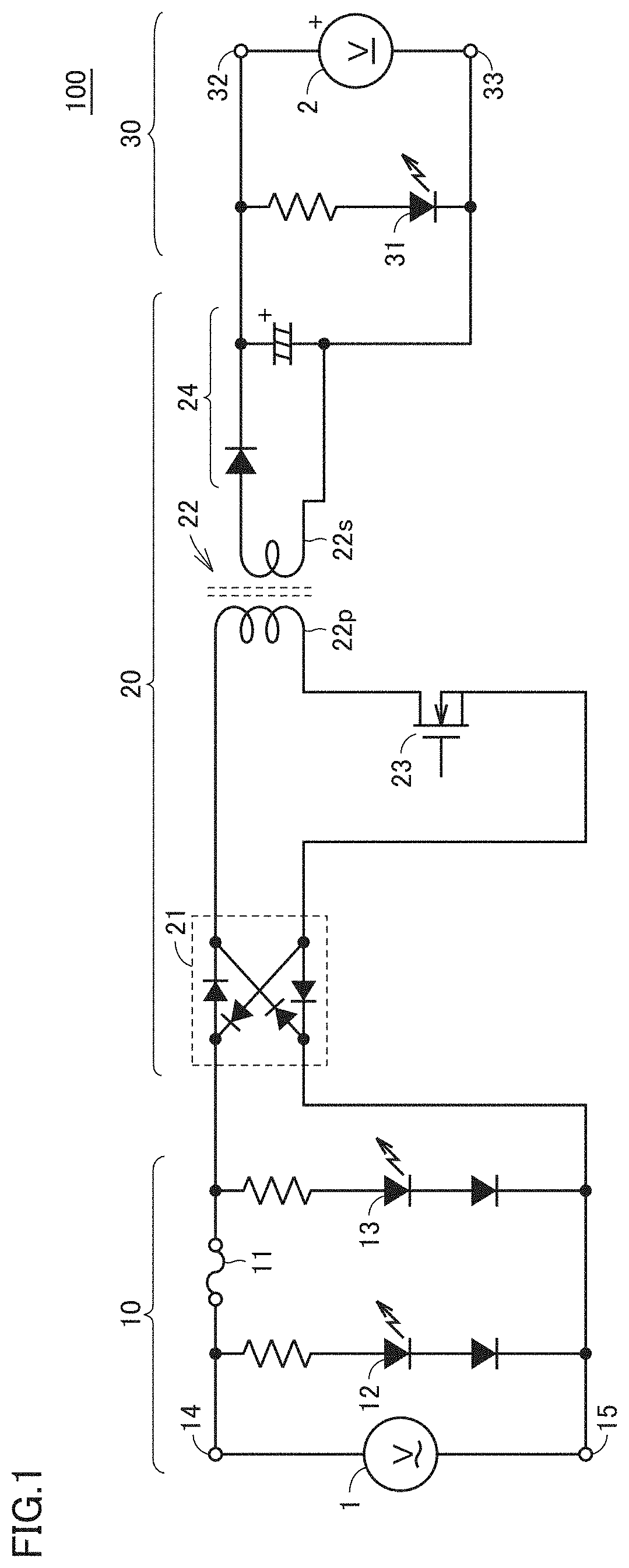
|---|---|---|
| Dec 5, 2017 | JP | 2017-233487 |
Claims
1. A power supply device, comprising: an input unit which includes an input terminal and a protection circuit connected to the input terminal; a power supply unit that generates a supply voltage from a voltage input through the input unit; an output unit which includes an output terminal which outputs the supply voltage; a first output circuit that generates a first output in response to input of a voltage to the input terminal, the first output circuit being disposed between the input terminal and the protection circuit; a second output circuit that generates a second output in response to input of a voltage to the power supply unit through the protection circuit, the second output circuit being disposed between the protection circuit and the power supply unit; and a third output circuit that generates a third output in response to output from the power supply unit, the third output circuit being connected to the output terminal wherein the first output circuit, the second output circuit, and the third output circuit are light-emitting circuits, and the first output, the second output, and the third output are light outputs, and the first output circuit turns on in response to an input voltage exceeding a threshold voltage.
2. (canceled)
3. The power supply device according to claim 1, wherein the power supply unit includes: a transformer having a primary winding, an auxiliary winding, and a secondary winding; a switching element connected to the primary winding of the transformer; and a drive control circuit that receives a voltage across the auxiliary winding of the transformer and drives the switching element, the power supply device further comprising a fourth output circuit that outputs a fourth signal indicating whether the voltage across the auxiliary winding is normal.
4. The power supply device according to claim 3, wherein the fourth output circuit is a light-emitting circuit and the fourth output is a light output.
5. The power supply device according to claim 1, further comprising a display circuit that displays information regarding a state of the power supply device, based at least on the first output, the second output, and the third output.
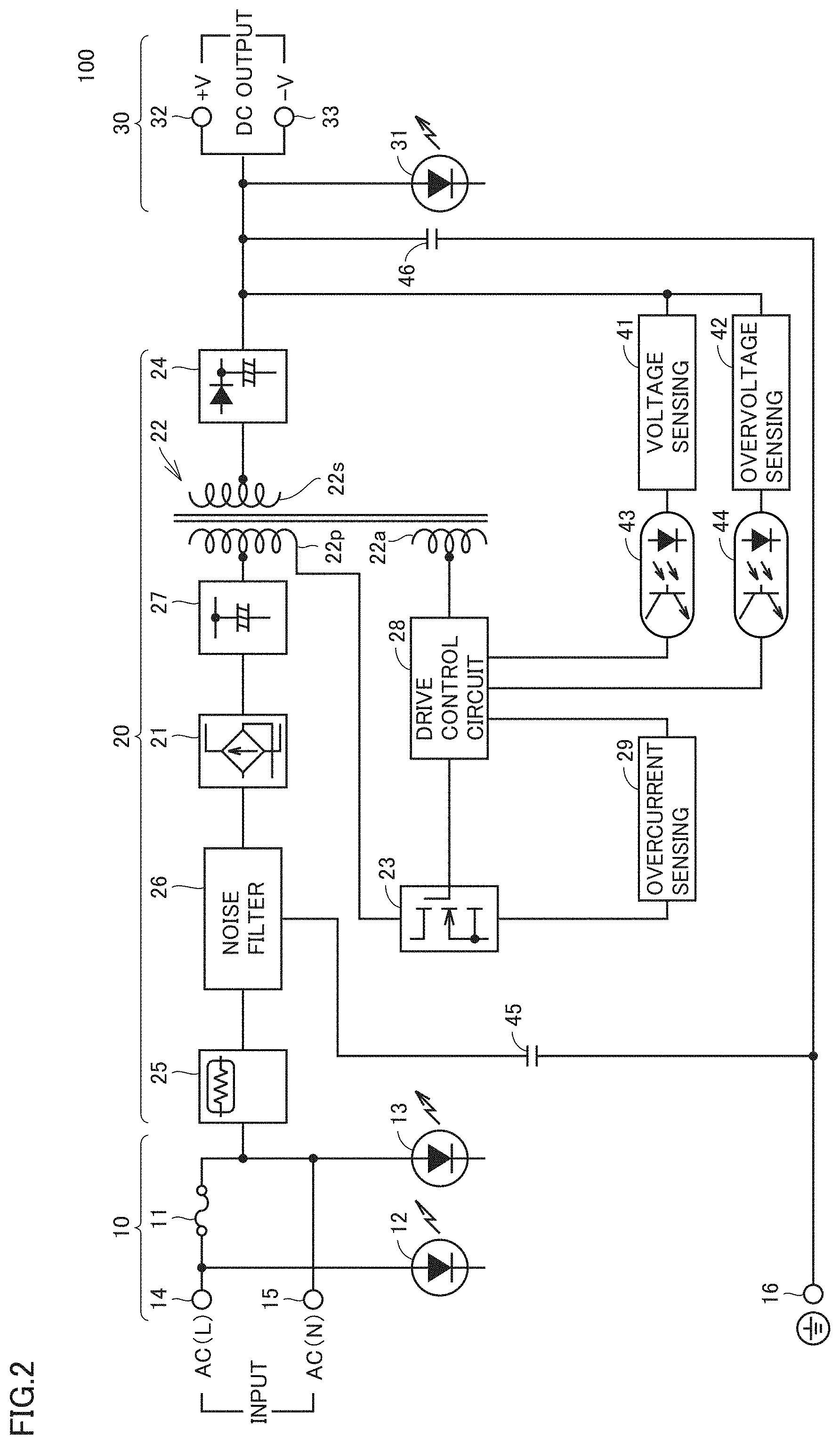
Description
TECHNICAL FIELD
[0001] The present invention relates to a power supply device.
BACKGROUND ART
[0002] For example, Japanese Patent Laying-Open No. 2006-349626 (PTL 1) discloses a mount circuit having a configuration which allows a user to readily find an anomaly, such as a reduction in supply voltage. The mount circuit includes an LED element for monitoring the state of the supply voltage and an illumination control circuit for the LED element. The illumination control circuit turns the LED element on if the supply voltage is greater than or equal to a given voltage. The illumination control circuit turns the LED element off if the supply voltage is less than the given voltage.
CITATION LIST
Patent Literature
[0003] PTL 1: Japanese Patent Laying-Open No. 2006-349626
SUMMARY OF INVENTION
Technical Problem
[0004] According to the above configuration, a user can ascertain the state of output of the power supply device. However, in the event of an anomaly in a circuit included in the power supply device, the circuit needs to be inspected with a measuring instrument, such as a tester, in order to identify the cause of the anomaly.
[0005] An object of the present invention is to provide a power supply device which allows a user to readily confirm the internal state of the power supply device.
Solution to Problem
[0006] According to one example of the present disclosure, a power supply device includes: an input unit which includes an input terminal and a protection circuit connected to the input terminal; a power supply unit that generates a supply voltage from a voltage input through the input unit; an output unit which includes an output terminal which outputs the supply voltage; a first output circuit that generates a first output in response to input of a voltage to the input terminal, the first output circuit being disposed between the input terminal and the protection circuit; a second output circuit that generates a second output in response to input of a voltage to the power supply unit through the protection circuit, the second output circuit being disposed between the protection circuit and the power supply unit; and a third output circuit that generates a third output in response to output from the power supply unit, the third output circuit being connected to the output terminal.
[0007] According to the above configuration, the power supply device can be provided which allows a user to readily confirm the internal state of the power supply device. The user is allowed to confirm an anomaly with respect to input of the power supply device from the first output from the first output circuit. The user is allowed to confirm whether the protection circuit is operating normally from the second output from the second output circuit. The user is allowed to confirm whether the power supply unit is operating normally from the third output from the third output circuit. Note that the form of "output" is not particularly limited, and may be an electrical output or a light output, for example.
[0008] In the power supply device, the first output circuit, the second output circuit, and the third output circuit are light-emitting circuits, and the first output, the second output, and the third output are light outputs.
[0009] According to the above configuration, the state of the power supply device can be notified outside the power supply device. The type of the light-emitting circuit is not particularly limited.
[0010] In the power supply device, the power supply unit includes: a transformer having a primary winding, an auxiliary winding, and a secondary winding; a switching element connected to the primary winding of the transformer; and a drive control circuit that receives a voltage across the auxiliary winding of the transformer and drives the switching element, the power supply device further comprising a fourth output circuit that outputs a fourth signal indicating whether the voltage across the auxiliary winding is normal.
[0011] According to the above configuration, the power supply device can be provided which allows a user to readily confirm the operative state of the power supply unit. For example, when a multiple number of the power supply devices are used to drive the load, the load can be driven by all the power supply devices if no difference is caused in output voltage between the power supply devices. In contrast, if differences are caused in output voltage between the power supply devices, the operation of a power supply device, whose output voltage is low, stops. In other words, the power supply unit is deactivated. Accordingly, a user can readily confirm the power supply device in operation and the deactivated power supply device.
[0012] In the above power supply device, the fourth output circuit is a light-emitting circuit and the fourth output is a light output.
[0013] According to the above configuration, the state of the power supply device can be notified outside the power supply device.
[0014] The power supply device further includes a display circuit that displays information regarding a state of the power supply device, based at least on the first output, the second output, and the third output.
[0015] According to the above configuration, a user can ascertain the state of the power supply device from the information (e.g., an error code) displayed on the display circuit. The type of the display circuit is not limited.
Advantageous Effects of Invention
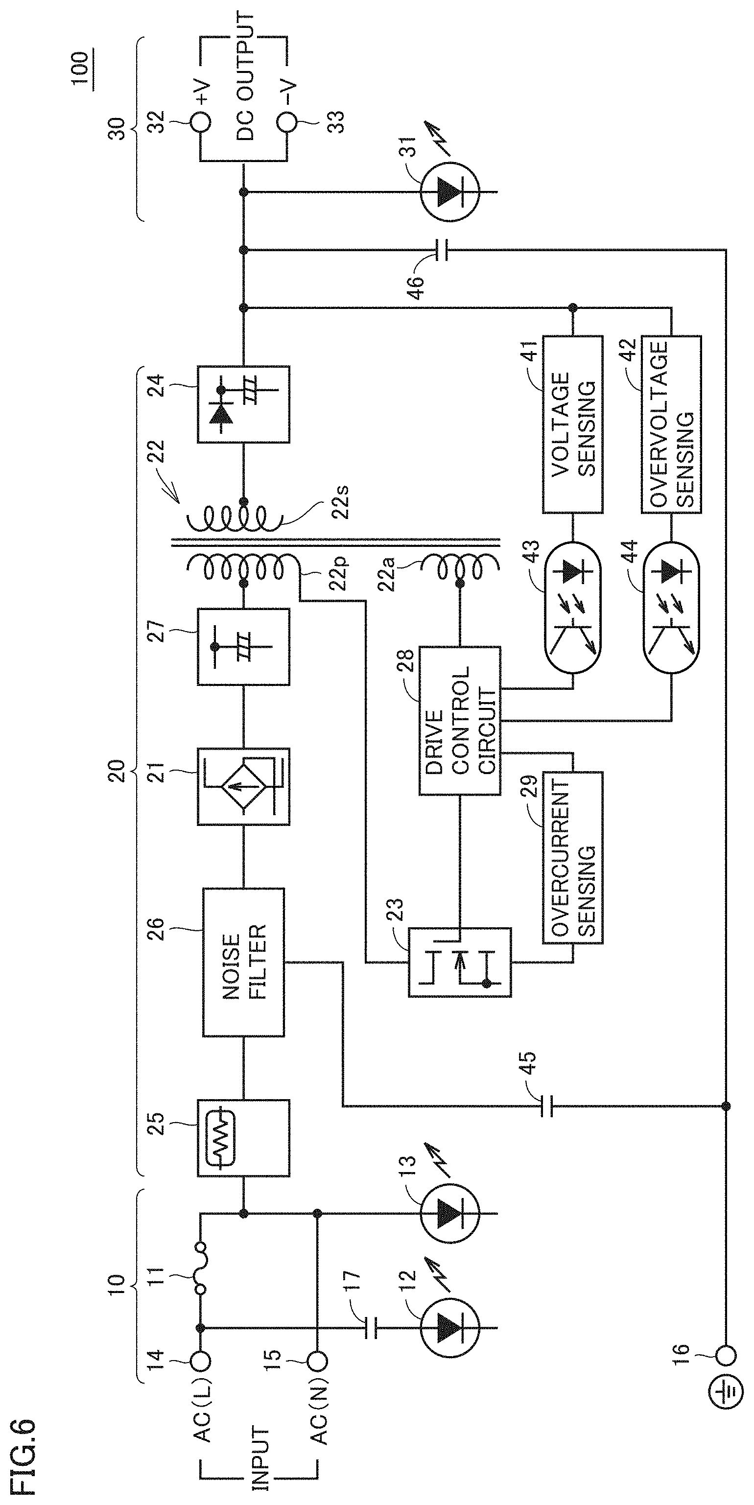
[0016] According to one example of the present disclosure, the power supply device can be provided which allows a user to readily confirm the internal state of the power supply device.
BRIEF DESCRIPTION OF DRAWINGS
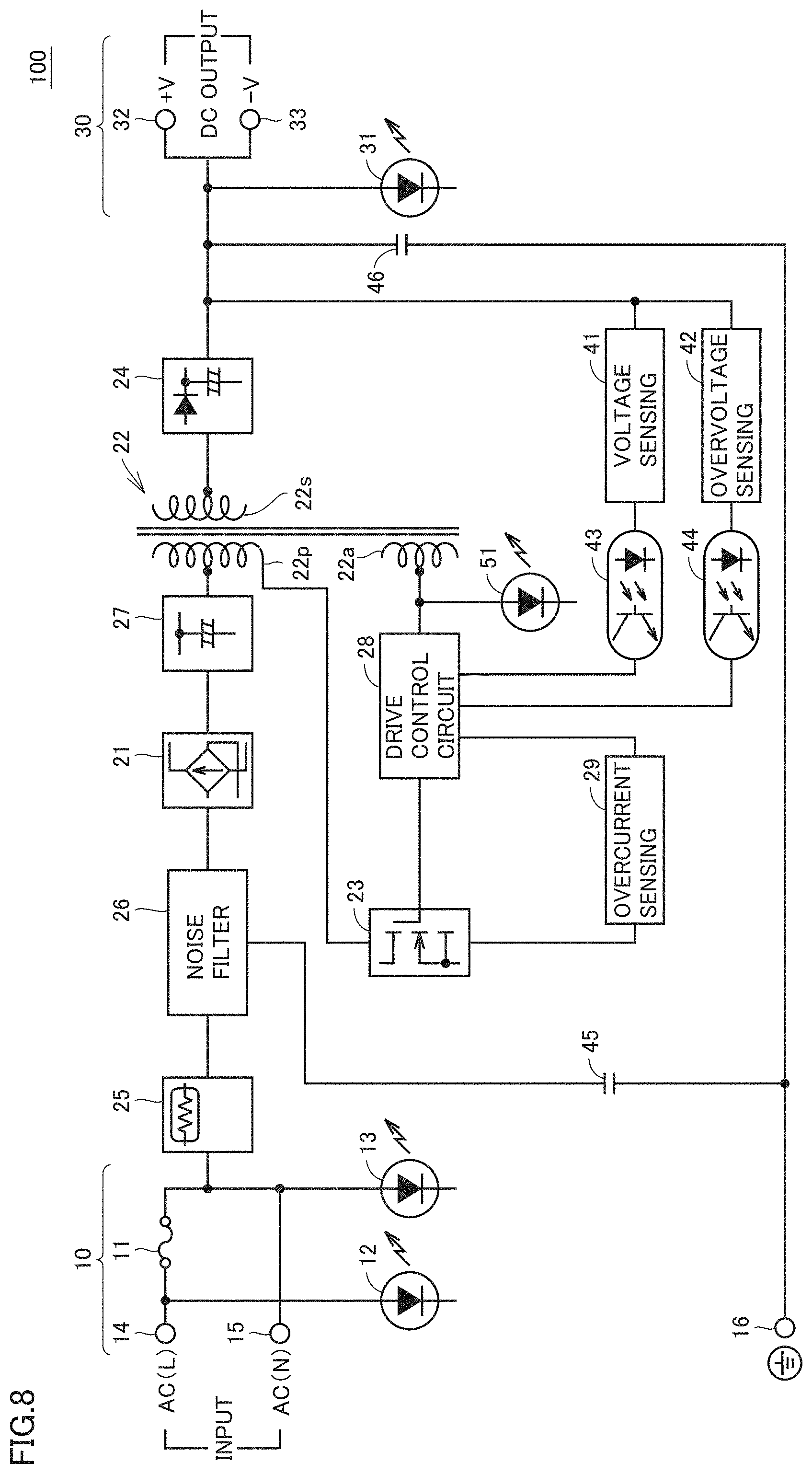
[0017] FIG. 1 is a circuit diagram showing a schematic configuration of a power supply device 100 according to an embodiment of the present disclosure.
[0018] FIG. 2 is a block diagram showing one example configuration of power supply device 100 of FIG. 1.
[0019] FIG. 3 is a diagram illustrating patterns of illumination of LEDs according to one embodiment.
[0020] FIG. 4 is a diagram illustrating patterns of illumination of the LEDs when lighting conditions for an input 1 has a threshold.
[0021] FIG. 5 is a diagram illustrating patterns of illumination of the LEDs when lighting conditions for an input 2 has a threshold.
[0022] FIG. 6 is a diagram showing another example configuration of power supply device 100 according to the embodiment of the present disclosure.
[0023] FIG. 7 is a circuit diagram showing still another example configuration of power supply device 100 according to the embodiment of the present disclosure.
[0024] FIG. 8 is a block diagram showing one example configuration of power supply device 100 of FIG. 7.
[0025] FIG. 9 is a schematic diagram schematically illustrating parallel operation by multiple power supply devices 100.
[0026] FIG. 10 is a schematic diagram illustrating the parallel operation by multiple power supply devices 100 while a difference is caused in output voltage.
[0027] FIG. 11 is a schematic diagram illustrating the parallel operation by multiple power supply devices 100 while no difference is caused in output voltage.
[0028] FIG. 12 is a diagram showing patterns of the combination of signals from four photocouplers.
[0029] FIG. 13 is a diagram schematically showing one example of appearance of the power supply device according to the embodiment of the present invention.
DESCRIPTION OF EMBODIMENTS
[0030] In the following, the present embodiment will be described in detail, with reference to the accompanying drawings. Note that like reference signs are used to refer to like or corresponding parts in the drawings.
.sctn. 1 Application
[0031] Initially, referring to FIG. 1, one example scenario to which the present invention is applied will be described. FIG. 1 is a circuit diagram showing a schematic configuration of a power supply device 100 according to the present embodiment. Note that, in the description below, "connect" is not limited to direct connection and encompasses indirect connection via an element.
[0032] As shown in FIG. 1, power supply device 100 is a switching power supply device, for example. Power supply device 100 includes an input unit 10, a power supply unit 20, and an output unit 30.
[0033] For example, input unit 10 is connected to an alternating-current (AC) power supply (e.g., a commercial power supply at 50 Hz/60 Hz and 100 V/200 V) 1. Input unit 10 includes input terminals 14, 15, and a fuse 11 connected to input terminal 14. Fuse 11 is one example of a protection circuit according to the present embodiment.
[0034] Power supply unit 20 generates a supply voltage from a voltage input thereto through input unit 10. As one example, power supply unit 20 includes a rectifier circuit 21, a transformer 22, a MOSFET 23 as a switching element, and a rectifier/smoothing circuit 24. Details of power supply unit 20 will be described below.
[0035] Output unit 30 outputs a supply voltage generated by power supply unit 20. Output unit 30 includes output terminals 32, 33. In the configuration shown in FIG. 1, a direct-current (DC) voltage is output as the supply voltage. In order to represent the output of the DC voltage, output unit 30 is connected to a virtual DC power supply 2 in FIG. 1.
[0036] Power supply device 100 further includes LED 12, LED 13, and LED 31. LED 12 is one example of a first output circuit. The first output circuit is disposed between input terminal 14 and fuse 11 and generates a first output in response to input of a voltage to input terminal 14. LED 13 is one example of a second output circuit. The second output circuit is disposed between fuse 11 and power supply unit 20 and generates a second output in response to input of a voltage to power supply unit 20 through fuse 11. LED 31 is one example of a third output circuit. The third output circuit is connected to output terminals 32, 33 and generates a third output in response to output from power supply unit 20. In the example shown in FIG. 1, the "first output," "second output," and "third output" are, all, light outputs.
[0037] Note that a resistor and a diode are connected in series with each of LEDs 12, 13 in the example shown in FIG. 1. A resistor is connected in series with LED 31. However, the present disclosure is not limited such a configuration. LED 12 is on when AC power is input to input unit 10. LED 13 is on when fuse 11 is operating normally. LED 31 is on when DC power is output from output unit 30.
[0038] Suppose that LEDs 12, 13 are omitted and only LED 31 is included in power supply device 100. In the event of LED 31 being turned off, there is no way of knowing, without the use of a measuring instrument such as a tester, whether no alternating current is input to input unit 10 or fuse 11 is blown. According to the present embodiment, a user is allowed to visually confirm the internal state of the power supply device 100 and the state of the input voltage from the combination of on and off of LED 12, LED 13, and LED 31. Accordingly, a power supply device can be implemented which allows the user to readily confirm the internal state of the power supply device.
.sctn. 2 Example Configuration
[0039] FIG. 2 is a block diagram showing one example configuration of power supply device 100 of FIG. 1. An AC voltage is input to input terminals 14, 15 (INPUT). An input terminal 16 is a ground terminal.
[0040] In addition to the elements shown in FIG. 1, power supply unit 20 includes an inrush current-limiting circuit 25, a noise filter 26, a smoothing circuit 27, a drive control circuit 28, an overcurrent sensing circuit 29, a voltage sensing circuit 41, an overvoltage sensing circuit 42, a photocoupler 43, a photocoupler 44, and capacitors 45, 46.
[0041] Inrush current-limiting circuit 25 is configured of, for example, a resistor and a relay inserted in parallel with the resistor. The relay opens for tens of milliseconds since activation of power supply device 100 to prevent inrush current, after which the relay closes and power supply unit 20 is activated.
[0042] Noise filter 26 filters a high-frequency noise component superimposed on the AC voltage input to INPUT, and supplies rectifier circuit 21 with the AC voltage having the noise component removed therefrom. Smoothing circuit 27 is configured of a smoothing capacitor. Smoothing circuit 27 smooths the full-wave rectified voltage.
[0043] Transformer 22 includes a primary winding 22p, a secondary winding 22s, and an auxiliary winding 22a. Transformer 22 induces a high-frequency pulse voltage across primary winding 22p to secondary winding 22s and auxiliary winding 22a. The high-frequency pulse voltage induced to secondary winding 22s is utilized for DC output. The high-frequency pulse voltage induced to auxiliary winding 22a is utilized to activate the drive control circuit 28.
[0044] Rectifier/smoothing circuit 24 is configured of a smoothing capacitor and a half-wave rectifier circuit formed of a diode. Rectifier/smoothing circuit 24 half-rectifies the high-frequency, pulsed power source (the AC power source) induced to secondary winding 22s of transformer 22 to generate a DC output power source having specified output voltage and output current.
[0045] Voltage sensing circuit 41 detects the output voltage of the DC output power source by a corresponding step-down voltage. Photocoupler 43 outputs to drive control circuit 28 a signal corresponding to the detected step-down voltage. If the output voltage of the DC output power source exceeds a specified voltage, overvoltage sensing circuit 42 detects an overvoltage. Photocoupler 44 outputs to drive control circuit 28 a signal indicating the detection of overvoltage.
[0046] Drive control circuit 28 is configured of an control IC which includes a PWM (Pulse Width Modulation) signal generator, a feedback control circuit, an OCP (Over Current Protect) terminal, a switching drive terminal, a drive power supply terminal, etc. Drive control circuit 28 supplies a PWM signal to the gate of MOSFET 23 to drive MOSFET 23.
[0047] The secondary-side voltage, which is detected by voltage sensing circuit 41, is fed back to drive control circuit 28 via photocoupler 43. Drive control circuit 28 changes the duty ratio of the PWM signal based on the voltage fed back, and drives MOSFET 23 so that the supply voltage, which is the output voltage of the DC output power source, is the specified voltage.
[0048] MOSFET 23 is connected in series with primary winding 22p of transformer 22. In response to the PWM signal supplied from drive control circuit 28, MOSFET 23 interrupts the primary-side voltage to cause primary winding 22p of transformer 22 to generate a high-frequency, pulsed power source. The supply voltage generated by power supply unit 20 is output through output terminals 32, 33 (DC OUTPUT).
[0049] FIG. 3 is a diagram illustrating patterns of illumination of LEDs, according to one embodiment. The "input 1," "input 2," and "output 1," indicated in FIG. 3, respectively represent LED 12, LED 13, and LED 31.
[0050] Note that FIG. 3 illustrates all patterns of illumination of the LEDs. As illustrated in FIG. 3, LEDs 12, 13, 31 each have two states, on or off. Accordingly, 2.times.2.times.2=8 different patterns exist as a whole. Each LED is on when there is input of voltage, and off when not voltage is input.
[0051] Pattern 1 is a pattern in which input 1, input 2, and output 1 are all on, indicating that power supply device 100 is operating normally. Power supply device 100 is in the normal state.
[0052] Pattern 2 is a pattern in which input 1 and input 2 are on and output 1 is off, indicating that there is an anomaly on the secondary side of power supply unit 20 (e.g., there may be a short circuit on the output side, a failure on the secondary side, etc.).
[0053] Pattern 3 is a pattern in which input 1 and output 1 are on and input 2 is off. However, the internal state of the power supply device 100 that corresponds to such a pattern does not exist.
[0054] Pattern 4 is a pattern in which input 1 is on and input 2 and output 1 are off. Pattern 4 represents that there is an anomaly, such as blowout of fuse 11, a failure on the primary side of power supply unit 20, etc.
[0055] Pattern 5 is a pattern in which input 1 is off and input 2 and output 1 are on. Pattern 5 represents that power supply device 100 is in hold time. In practice, such a state may not take place.
[0056] Pattern 6 is a pattern in which input 1 and output 1 are off and input 2 is on. However, the internal state of the power supply device 100 that corresponds to such a pattern does not exist.
[0057] Pattern 7 is a pattern in which input 1 and input 2 are off and output 1 is on. Such a state can take place if, for example, a voltage external to power supply device 100 is applied to power supply device 100.
[0058] Pattern 8 is a pattern in which input 1, input 2, and output 1 are all off, indicating that there is no input voltage.
[0059] A certain threshold may exist for the voltage for switching input 1 between on/off. In other words, input 1 is on if the input voltage exceeds the threshold, and input 1 is off if the input voltage is less than or equal to the threshold. A correspondence between patterns of illumination of the LEDs according to such conditions and the internal states of the power supply device 100 will be described, with reference to FIG. 4.
[0060] FIG. 4 is a diagram illustrating patterns of illumination of the LEDs when lighting conditions for input 1 has a threshold. As illustrated in FIG. 4, the internal states of the power supply device 100 that correspond to patterns 5 and 6 are different from the example illustrated in FIG. 3. Specifically, pattern 5 (input 1 is off and input 2 and output 1 are on) indicates that power supply device 100 is in hold time or the input voltage of power supply device 100 has decreased. Pattern 6 (input 1 and output 1 are off and input 2 is on) indicates that the input voltage has decreased less than or equal to an operating stop voltage.
[0061] Similarly, a certain threshold may exist for the voltage for switching input 2 between on/off. In other words, input 2 is on if the input voltage exceeds the threshold, and input 2 is off if the input voltage is less than or equal to the threshold. A correspondence between patterns of illumination of the LEDs according to such conditions and the internal states of the power supply device 100 will be described, with reference to FIG. 5.
[0062] FIG. 5 is a diagram illustrating patterns of illumination of the LEDs when lighting conditions for input 2 has a threshold. As illustrated in FIG. 5, the internal state of the power supply device 100 that corresponds to pattern 3 is different from the example illustrated in FIG. 4. In the example shown in FIG. 5, pattern 3 (input 1 and output 1 are off and input 2 is on) indicates that the input voltage of power supply device 100 has decreased.
[0063] The configuration of power supply device 100 according to the present embodiment is not limited to the above. FIG. 6 is a diagram showing another example configuration of power supply device 100 according to the present embodiment. As shown in FIG. 6, an input capacitor 17 may be added to input unit 10. Input capacitor 17 is connected between the input terminal and LED 12. This allows the user to confirm whether a direct current is input to input unit 10 or an alternating current is input to input unit 10. The rest of the configuration of power supply device 100 shown in FIG. 6 is the same as the corresponding portion of the configuration shown in FIG. 2.
[0064] Moreover, multiple power supply devices 100 may be setup and the parallel operation may be performed. According to the present embodiment, the user is allowed to confirm for each of the multiple power supply devices 100 whether power supply device 100 is in operation or deactivated. A configuration for this will be described below.
[0065] FIG. 7 is a circuit diagram showing still another example configuration of power supply device 100 according to the present embodiment. FIG. 8 is a block diagram showing one example configuration of power supply device 100 shown in FIG. 7. As shown in FIGS. 7 and 8, power supply device 100 includes an LED 51 connected to auxiliary winding 22a of transformer 22. LED 51 is one example of a "fourth display circuit" according to the present embodiment.
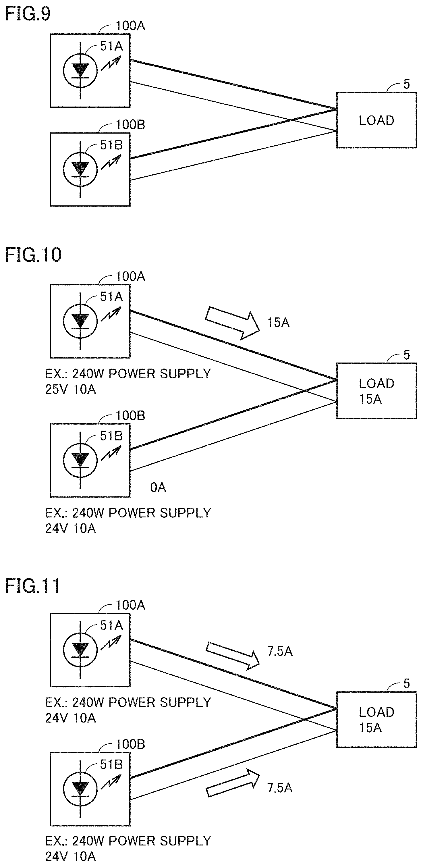
[0066] FIG. 9 is a schematic diagram schematically showing parallel operation by multiple power supply devices 100. For example, suppose that two power supply devices 100A, 100B are connected in parallel with a load 5. In this case, the output voltage needs to be set for each of power supply devices 100A, 100B so that there is no difference in output voltage between power supply devices 100A, 100B.
[0067] FIG. 10 is a schematic diagram showing the parallel operation by multiple power supply devices 100 while a difference is caused in output voltage between power supply devices 100. If a difference is caused in output voltage between power supply devices 100A, 100B, the output to load 5 is provided by the power supply device at a higher voltage. For example, suppose that power supply devices 100A, 100B are both a 240 W power supply, and the output voltage of power supply device 100A is 25 V whereas the output voltage of power supply device 100B is 24 V. In this case, a current (e.g., 15A) is supplied to load 5 only from power supply device 100A. In contrast, the switching operation of power supply device 100B is stopped. LED 51A included in power supply device 100A is on. In contrast, LED 51B included in power supply device 100B is off. Accordingly, the user is allowed to ascertain that power supply device 100B is not operating.
[0068] FIG. 11 is a schematic diagram showing the parallel operation by multiple power supply devices 100 while no difference is caused in output voltage. The output voltage is set for each of power supply devices 100A, 100B so that no difference is caused in output voltage between power supply devices 100A, 100B. Each of power supply devices 100A, 100B can output a voltage while retaining the equality in output between power supply devices 100A, 100B. LED 51A included in power supply device 100A and LED 51B included in power supply device 100B are both on and the user is thus allowed to ascertain that both power supply devices 100A, 100B are in operation.
[0069] Note that, in the circuit structure shown in FIGS. 7 and 8, LED 12, LED 13, LED 31, and LED 51 may be replaced with photocouplers. Each photocoupler corresponds to an "output circuit" according to the present invention. Signals output from the photocouplers respectively correspond to the "first output," "second output," "third output," and "fourth output." These signals can be conveyed to the control circuit (e.g., CPU) of power supply device 100. The user is allowed to confirm, from the combination of the signals from the four photocouplers, which type of malfunction has occurred in power supply device 100.
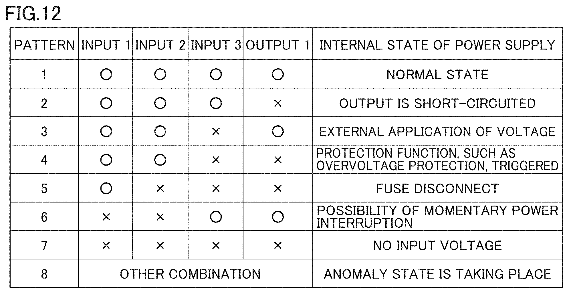
[0070] FIG. 12 is a diagram showing patterns of the combination of the signals from the four photocouplers. The "input 1," "input 2," "input 3," and "output 1," indicated in FIG. 12, represent the photocouplers alternative to LED 12, LED 13, LED 51, and LED 31, respectively. The sign "o" in FIG. 12 represents that the photocoupler outputs a signal. The sign "x" represents that the photocoupler outputs no signal.
[0071] Pattern 1 is a pattern in which all the photocouplers, which are input 1, input 2, input 3, and output 1, output signals, indicating that power supply device 100 is operating normally. The internal state of the power supply device 100 is in the normal state.
[0072] Pattern 2 is a pattern in which input 1, input 2, and input 3 output signals and output 1 outputs no signal, representing that there is an anomaly on the secondary side of power supply unit 20, for example, a short circuit on the output side.
[0073] Pattern 3 is a pattern in which input 1, input 2, and output 1 output signals and input 3 outputs no signal. Such a state can take place if, for example, a voltage external to power supply device 100 is applied to power supply device 100.
[0074] Pattern 4 is a pattern in which input 1 and input 2 output signals and input 3 and output 1 output no signal. Pattern 5 represents that a protection function, for example, overvoltage protection, has been triggered.
[0075] Pattern 5 is a pattern in which input 1 outputs a signal and input 2, input 3, and output 1 output no signal. Pattern 5 represents an anomaly, such as blowout of fuse 11, a failure on the primary side of power supply unit 20, etc.
[0076] Pattern 6 is a pattern in which input 1 and input 2 output no signal and input 3 and output 1 output signals. Pattern 6 represents that momentary power interruption may have occurred in power supply device 100.
[0077] Pattern 7 is a pattern in which input 1, input 2, input 3, and output 1 output no signal. Such a state can take place if, for example, there is no voltage input to power supply device 100.
[0078] Pattern 8 is a pattern of a combination of signals, other than the combinations described above. An anomaly state is taking place in power supply device 100 if the pattern of the combination of signals corresponds to pattern 8.
[0079] As still another configuration, information as to whether a surge has been input may be held instantly. For example, a reference voltage that is proportional to the input voltage may be generated and the power supply device may be latched if the reference voltage has exceeded, even instantly, a certain value. The LED display pattern or display mode in this case is not particularly limited. For example, the LED (e.g., input 1) may be on in a display color different from a typical display color. Similarly, power supply device 100 may have a function of sensing a momentary power interruption. In this case, the power supply device may be latched and the LED (e.g., input 1) may be on in the display color different from the typical display color if the reference voltage has decreased below a certain value even instantly.
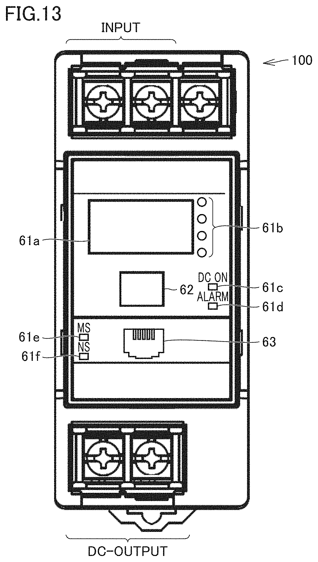
[0080] FIG. 13 is a diagram schematically showing one example of appearance of the power supply device according to the embodiment of the present invention. As shown in FIG. 13, display circuits 61a to 61f, a switch 62, and a communication circuit 63 are disposed on the surface of power supply device 100 on which the terminals for INPUT and the terminals for DC-OUTPUT are provided.
[0081] Display circuit 61a is configured of a 7-segment LED, for example. Display circuit 61a may be an LCD or an organic EL display, for example. As described above, if the first output circuit, the second output circuit, the third output circuit, and the fourth output circuit respectively corresponding to "input 1," "input 2," "input 3," "output 1," are each configured of a photocoupler, the 7-segment LED can implement a display circuit which displays, through the control by the CPU, information regarding the state of power supply device 100 based on the first output, the second output, and the third output. Note that, based on the configuration shown in FIGS. 1 and 2, display circuit 61a may display the information regarding the state of power supply device 100 based on the outputs (the first output, the second output, and the third output) from the first output circuit, the second output circuit, and the third output circuit corresponding to "input 1," "input 2," and "output 1," respectively.
[0082] Display circuit 61b is configured of the LED lamps aligned on the side of display circuit 61a. The number of LED lamps is not particularly limited. For example, two LED lamps may correspond to LED 12 (input 1) and LED 13 (input 2). Alternatively, three LED lamps may correspond to LED 12 (input 1), LED 13 (input 2), and LED 51 (input 3). Display circuit 61c is configured of the LED lamp located below the display circuit 61b. The LED lamp being on indicates that the DC voltage is output from power supply device 100. Display circuit 61c may correspond to LED 31 (output 1).
[0083] Display circuit 61d may be configured of the LED lamp located below the display circuit 61c and indicate that an anomaly is occurring in power supply device 100 by turning the LED lamp on.
[0084] Display circuit 61e and display circuit 61f are configured of the two LED lamps aligned on the side of communication circuit 63. These LED lamps being on indicate a status of communication by communication circuit 63.
[Effects]
[0085] As described above, in the present embodiment, the user is allowed to visually confirm the internal state of the power supply device 100 and the state of the input voltage at least from the combinations of the outputs from three output circuits.
[Supplementary Notes]
[0086] As described above, the present embodiment includes the disclosure as follows:
[0087] 1. A power supply device (100), including: [0088] an input unit (10) which includes an input terminal (14) and a protection circuit (11) connected to the input terminal (14); [0089] a power supply unit (20) that generates a supply voltage from a voltage input through the input unit (10); [0090] an output unit (30) which includes an output terminal (32) which outputs the supply voltage; [0091] a first output circuit (12) that generates a first output in response to input of a voltage to the input terminal (14), the first output circuit being disposed between the input terminal (14) and the protection circuit (11); [0092] a second output circuit (13) that generates a second output in response to input of a voltage to the power supply unit (20) through the protection circuit (11), the second output circuit being disposed between the protection circuit (11) and the power supply unit (20); and [0093] a third output circuit (31) that generates a third output in response to output from the power supply unit (20), the third output circuit being connected to the output terminal (32).
[0094] 2. The power supply device (100) according to 1, wherein [0095] the first output circuit (12), the second output circuit (13), and the third output circuit (31) are light-emitting circuits, and the first output, the second output, and the third output are light outputs.
[0096] 3. The power supply device (100) according to 1 or 2, wherein [0097] the power supply unit (20) includes: [0098] a transformer having a primary winding (22p), an auxiliary winding (22a), and a secondary winding (22s); [0099] a switching element (23) connected to the primary winding (22p) of the transformer; and [0100] a drive control circuit (28) that receives a voltage across the auxiliary winding (22a) of the transformer and drives the switching element (23), [0101] the power supply device (100) further including a fourth output circuit (31) that outputs a fourth signal indicating whether the voltage across the auxiliary winding (22a) is normal.
[0102] 4. The power supply device (100) according to 3, wherein [0103] the fourth output circuit (31) is a light-emitting circuit and the fourth output is a light output.
[0104] 5. The power supply device (100) according to 1, further including [0105] a display circuit that displays information regarding a state of the power supply device (100), based at least on the first output, the second output, and the third output.
[0106] While the embodiment according to the present invention has been described above, the embodiment presently disclosed should be considered in all aspects illustrative and not restrictive. The scope of the present invention is defined by the appended claims. All changes which come within the meaning and range of equivalency of the appended claims are to be embraced within their scope.
REFERENCE SIGNS LIST
[0107] 2 DC power supply; 5 load; 10 input unit; 11 fuse; 14, 15, 16 input terminal; 17 input capacitor; 20 power supply unit; 21 rectifier circuit; 22 transformer; 22a auxiliary winding; 22p primary winding; 22s secondary winding; 23 MOSFET; 24 rectifier/smoothing circuit; 25 inrush current-limiting circuit; 26 noise filter; 28 drive control circuit; 29 overcurrent sensing circuit; 30 output unit; 32, 33 output terminal; 41 voltage sensing circuit; 42 overvoltage sensing circuit; 43, 44 photocoupler; 45, 46 capacitor; 61a to 61f display circuit; 62 switch; 63 communication circuit; and 100, 100A, 100B power supply device.
* * * * *
D00000
D00001
D00002
D00003
D00004
D00005
D00006
D00007
D00008
D00009
XML
uspto.report is an independent third-party trademark research tool that is not affiliated, endorsed, or sponsored by the United States Patent and Trademark Office (USPTO) or any other governmental organization. The information provided by uspto.report is based on publicly available data at the time of writing and is intended for informational purposes only.
While we strive to provide accurate and up-to-date information, we do not guarantee the accuracy, completeness, reliability, or suitability of the information displayed on this site. The use of this site is at your own risk. Any reliance you place on such information is therefore strictly at your own risk.
All official trademark data, including owner information, should be verified by visiting the official USPTO website at www.uspto.gov. This site is not intended to replace professional legal advice and should not be used as a substitute for consulting with a legal professional who is knowledgeable about trademark law.