Buck Matrix-type Rectifier With Boost Switch, And Operation Thereof During One-phase Loss
AFSHARIAN; Jahangir ; et al.
U.S. patent application number 17/051538 was filed with the patent office on 2021-03-04 for buck matrix-type rectifier with boost switch, and operation thereof during one-phase loss. The applicant listed for this patent is Murata Manufacturing Co., Ltd.. Invention is credited to Jahangir AFSHARIAN, Bing GONG, Dewei XU.
| Application Number | 20210067053 17/051538 |
| Document ID | / |
| Family ID | 1000005252868 |
| Filed Date | 2021-03-04 |


View All Diagrams
| United States Patent Application | 20210067053 |
| Kind Code | A1 |
| AFSHARIAN; Jahangir ; et al. | March 4, 2021 |
BUCK MATRIX-TYPE RECTIFIER WITH BOOST SWITCH, AND OPERATION THEREOF DURING ONE-PHASE LOSS
Abstract
A power supply circuit includes at least two input terminals that receive an input voltage, a transformer including a primary side electrically connected to the input voltage, a rectifier electrically connected to a secondary side of the transformer, and a boost switch electrically connected in parallel with the rectifier and a pair of output voltage terminals that include a first output voltage terminal and a second output voltage terminal. The input voltage is electrically connected to an AC source, and each of the at least two input terminals receives a different phase of the AC source.
| Inventors: | AFSHARIAN; Jahangir; (Markham, CA) ; GONG; Bing; (Markham, CA) ; XU; Dewei; (Markham, CA) | ||||||||||
| Applicant: |
|
||||||||||
|---|---|---|---|---|---|---|---|---|---|---|---|
| Family ID: | 1000005252868 | ||||||||||
| Appl. No.: | 17/051538 | ||||||||||
| Filed: | April 30, 2019 | ||||||||||
| PCT Filed: | April 30, 2019 | ||||||||||
| PCT NO: | PCT/US2019/070004 | ||||||||||
| 371 Date: | October 29, 2020 |
Related U.S. Patent Documents
| Application Number | Filing Date | Patent Number | ||
|---|---|---|---|---|
| 62665180 | May 1, 2018 | |||
| Current U.S. Class: | 1/1 |
| Current CPC Class: | H02M 1/083 20130101; H02M 3/158 20130101; H02M 7/219 20130101 |
| International Class: | H02M 7/219 20060101 H02M007/219; H02M 1/08 20060101 H02M001/08; H02M 3/158 20060101 H02M003/158 |
Claims
1. A power supply circuit comprising: at least two input terminals that receive an input voltage; a transformer including a primary side electrically connected to the input voltage; a rectifier electrically connected to a secondary side of the transformer; and a boost switch electrically connected in parallel with the rectifier and a pair of output voltage terminals that include a first output voltage terminal and a second output voltage terminal; wherein the input voltage is electrically connected to an AC source, and each of the at least two input terminals receives a different phase of the AC source.
2. The power supply circuit according to claim 1, further comprising ORing diodes or Field Effect Transistors (FETs) that include a first terminal electrically connected to a first terminal of the boost switch and a second terminal electrically connected to the first output voltage terminal.
3. The power supply circuit according to claim 2, further comprising an output filter electrically connected to an output of the rectifier.
4. The power supply circuit according to claim 3, wherein the output filter includes an output inductor and an output capacitor.
5. The power supply circuit according to claim 4, wherein: the output inductor is electrically connected between the output of the rectifier and the first terminal of the boost switch; and the output capacitor is electrically connected between a node electrically connecting the second terminal of the ORing diodes or FETs and the first output voltage terminal and a node electrically connecting the second output voltage terminal and a second terminal of the boost switch.
6. The power supply circuit according to claim 1, wherein each of the different phases of the AC source are combined into a single phase on the primary side of the transformer.
7. The power supply circuit according to claim 6, wherein the different phases of the AC source are combined into the single phase by a matrix rectifier.
8. The power supply circuit according to claim 1, further comprising an input filter electrically connected between each of the at least two input terminals and the transformer.
Description
BACKGROUND OF THE INVENTION
1. Field of the Invention
[0001] The present invention relates to isolated matrix rectifiers. More specifically, the present invention relates to an isolated buck matrix rectifier with a boost switch and to the operation of the rectifier during the loss of one input voltage phase.
2. Description of the Related Art
[0002] FIG. 1 is a circuit diagram of an isolated buck matrix rectifier according to a related art. The matrix rectifier shown in FIG. 1 includes a 3-phase-to-1-phase matrix converter that is electrically connected to a rectifier. With respect to FIG. 1, a "line side" or "primary side" refers to the portion of the circuit on the left-hand side of a transformer Tr that is electrically connected to the input line voltages v.sub.a, vb, and v.sub.c and the input line currents i.sub.a, i.sub.b, and i.sub.c for each of the three phases A, B, and C, and a "load side" or a "secondary side" refers to the portion of the circuit on the right-hand side of the transformer Tr that is electrically connected to the output voltage V.sub.o, which may be electrically connected to a load (not shown).
[0003] On the line side of the circuit in FIG. 1, a three-phase alternating current (AC) input, including input line voltages v.sub.a, v.sub.b, and v.sub.c, is filtered by an input-side filter defined by input inductors L.sub.f and input capacitors C.sub.f and then combined into a single-phase AC current by the 3-phase-to-1-phase matrix converter. The 3-phase-to-1-phase matrix converter includes two pairs of complementary transistors, respectively S.sub.11-S.sub.16 and S.sub.21-S.sub.26, for each of the three phases A, B, and C and provides the single-phase AC voltage vp and the single-phase AC current i.sub.P on the primary side (line side) of the transformer Tr. A leakage inductance of the transformer Tr and/or an external inductor is indicated by L.sub.lk. On the load side of the circuit, the single-phase AC voltage vs and the single-phase AC current on the secondary side (load side) of the transformer Tr are rectified by the rectifier, which includes diodes D.sub.1, D.sub.2, D.sub.3, and D.sub.4, to provide a DC voltage V.sub.d and a DC current i.sub.L. An output inductor L.sub.o and an output capacitor C.sub.o define a load-side filter, and the load-side filter filters the DC voltage Vd and the DC current i.sub.L to provide the output voltage V.sub.o and an output current I.sub.o.
[0004] However, with the matrix rectifier shown in FIG. 1, the output voltage V.sub.o drops when the output voltage of the bridge rectifier (DC voltage Vd) is lower than the output voltage V.sub.o, because the matrix rectifier shown in FIG. 1 does not have any boost capability.
[0005] In matrix rectifiers, it is difficult to maintain a steady output voltage and to deliver continuous power when one phase is lost, disconnected, or short circuited due to the lack of an intermediate storage energy and a second stage DC/DC converter for output voltage regulation. Therefore, problems associated with matrix rectifiers that operate when one phase is lost, disconnected, or shorted include a large output drop. For example, matrix rectifiers are unlikely to sustain an output voltage within 5% of a nominal output voltage when one phase is lost, disconnected, or shorted. To address this problem, output capacitors with relatively high values have been used to attempt to sustain the output voltage when one phase is lost, disconnected, or shorted, but including large output capacitors significantly reduces the overall power density of the matrix rectifier circuitry and prevents the matrix rectifier from having a compact size. In addition, matrix rectifiers are subjected to high stress when delivering only 2/3 of their rated output power while one phase is lost, disconnected, or shorted.
SUMMARY OF THE INVENTION
[0006] To overcome the problems described above, preferred embodiments of the present invention provide an isolated buck matrix rectifier with a boost switch.
[0007] A power supply circuit according to a preferred embodiment of the present invention includes at least two input terminals that receive an input voltage, a transformer including a primary side electrically connected to the input voltage, a rectifier electrically connected to a secondary side of the transformer, and a boost switch electrically connected in parallel with the rectifier and a pair of output voltage terminals that include a first output voltage terminal and a second output voltage terminal. The input voltage is electrically connected to a three-phase AC source, and each of the at least two input terminals receives a different phase of the AC source.
[0008] Preferably, the power supply circuit further includes ORing diodes or Field Effect Transistors (FETs) that include a first terminal electrically connected to a first terminal of the boost switch and a second terminal electrically connected to the first output voltage terminal.
[0009] Preferably, the power supply circuit further includes an output filter electrically connected to an output of the rectifier.
[0010] Preferably, the output filter includes an output inductor and an output capacitor.
[0011] Preferably, the output inductor is electrically connected between the output of the rectifier and the first terminal of the boost switch, and the output capacitor is electrically connected between a node electrically connecting the second terminal of the ORing diodes or FETs and the first output voltage terminal and a node electrically connecting the second output voltage terminal and a second terminal of the boost switch.
[0012] Preferably, each of the different phases of the AC source are combined into a single phase on the primary side of the transformer. The different phases of the AC source are preferably combined into the single phase by a matrix rectifier.
[0013] Preferably, the power supply circuit further includes an input filter electrically connected between each of the at least two input terminals and the transformer.
[0014] Isolated buck matrix rectifiers each with a boost switch according to the preferred embodiments of the present invention are able to significantly reduce or prevent a drop in the output voltage compared with a nominal output voltage and to significantly reduce an output capacitance. Further, isolated buck matrix rectifiers each with a boost switch according to the preferred embodiments of the present invention are able to provide a high power density in a compact size, while also significantly reducing a current stress on the included circuit components.
[0015] The above and other features, elements, steps, configurations, characteristics and advantages of the present invention will become more apparent from the following detailed description of preferred embodiments of the present invention with reference to the attached drawings.
BRIEF DESCRIPTION OF THE DRAWINGS
[0016] FIG. 1 is a circuit diagram of an isolated buck matrix rectifier according to a related art.
[0017] FIG. 2 is a circuit diagram of an isolated buck matrix rectifier with a boost switch according to a preferred embodiment of the present invention.
[0018] FIG. 3A is a circuit diagram of a three-phase converter of the isolated buck matrix rectifier shown in FIG. 2 redrawn as a zero voltage switching (ZVS) full-bridge DC-DC converter. FIG. 3B is a circuit diagram of the three-phase converter shown in FIG. 3A when one of the phases is not present.
[0019] FIGS. 4(a)-4(d) are graphs showing waveforms of voltage and current characteristics over time of a three-phase rectifier with a boost switch during one-phase-loss operation according to a preferred embodiment of the present invention.
[0020] FIGS. 5A and 5B are graphs comparing an output voltage drop in one-phase-loss operation with a boost switch according to a preferred embodiment of the present invention to an output voltage drop in one-phase-loss operation without a boost switch.
[0021] FIGS. 6(a)-6(e) are graphs showing simulated waveforms of voltage and current characteristics over time of a three-phase rectifier with a boost switch when one phase is shorted and then recovered, according to a preferred embodiment of the present invention.
[0022] FIGS. 7(a)-7(d) are graphs showing experimental waveforms of a voltage converter including a three-phase rectifier with a boost switch both during three-phase operation and during two-phase operation, according to a preferred embodiment of the present invention.
DETAILED DESCRIPTION OF PREFERRED EMBODIMENTS
[0023] Preferred embodiments of the present invention will now be described in detail with reference to FIGS. 2 to 7(d). Note that the following description is in all aspects illustrative and not restrictive and should not be construed to restrict the applications or uses of preferred embodiments of the present invention in any manner.
[0024] FIG. 2 is a circuit diagram of an isolated buck matrix rectifier with a boost switch according to a preferred embodiment of the present invention. In contrast to the isolated buck matrix rectifier shown in FIG. 1, the isolated buck matrix rectifier shown in FIG. 2 includes a boost switch.
[0025] The isolated buck matrix rectifier shown in FIG. 2 includes a 3-phase-to-1-phase matrix converter that is electrically connected to a rectifier. With respect to FIG. 2, a "line side" or "primary side" refers to the portion of the circuit on the left-hand side of a transformer Tr that is electrically connected to the input line voltages v.sub.a, v.sub.b, and v.sub.c and the input line currents i.sub.a, i.sub.b, and i.sub.c for each of the three phases A, B, and C, and a "load side" or "secondary side" refers to the portion of the circuit on the right-hand side of the transformer T.sub.r that is electrically connected to the output voltage V.sub.o, which may be electrically connected to a load (not shown).
[0026] On the line side of the circuit in FIG. 2, a three-phase alternating current (AC) input, including input line voltages v.sub.a, v.sub.b, and v.sub.c, is filtered by an input-side filter defined by input inductors L.sub.f and input capacitors C.sub.f and then combined into a single-phase AC current by the 3-phase-to-1-phase matrix converter. The 3-phase-to-1-phase matrix converter includes two pairs of complementary transistors, respectively S.sub.11-S.sub.16 and S.sub.21-S.sub.26, for each of the three phases A, B, and C and provides the single-phase AC voltage vp and the single-phase AC current i.sub.p on the primary side (line side) of the transformer Tr. A leakage inductance of the transformer Tr and/or an external inductor is indicated by L.sub.lk. On the load side of the circuit, the single-phase AC voltage vs and the single-phase AC current on the secondary side (load side) of the transformer Tr are rectified by the rectifier, which includes diodes D.sub.1, D.sub.2, D.sub.3, and D.sub.4, to provide a DC voltage V.sub.d and a DC current i.sub.L. An output inductor L.sub.o and an output capacitor C.sub.o define a load-side filter, and the load-side filter filters the DC voltage V.sub.d and the DC current i.sub.L to provide the output voltage V.sub.o and an output current I.sub.o.
[0027] As shown in FIG. 2, a boost switch S.sub.boost and ORing device(s) are provided between the output inductor L.sub.o and the output capacitor C.sub.o to define a boost stage. The boost switch S.sub.boost can be a metal-oxide-semiconductor field-effect transistor (MOSFET) or the like, and the ORing devices can be diodes, field-effect transistors (FETs), or the like. In FIG. 2, the ORing devices are shown as a single diode between the output inductor L.sub.o and the output voltage V.sub.o, but it should be understood that instead of the diode, one or more FETs in parallel can be used.
[0028] The ORing devices are conventionally used in redundant power supply systems or in systems with multiple power supplies to prevent reverse current. For example, if first and second AC-DC converters are connected in parallel, then ORing devices at the output of each of the first and second converters allow current from the first and second converters to flow to the load, while preventing current from the second or first converter from entering the other of the first or second converter. In FIG. 2, the ORing devices, in addition to providing the ORing functions described above, function as a boost diode with synchronous rectification when the DC voltage Vd of the bridge rectifier is lower than the output voltage V.sub.o.
[0029] Conventionally, the ORing devices are located after the output capacitors, and boost converters generally require both boost switches and boost diodes. However, in FIG. 2, the output capacitor C.sub.o is located after the ORing devices. By connecting the output capacitor C.sub.O after the ORing devices as shown in FIG. 2, the ORing devices can operate as boost diodes. Thus, because no additional diodes are required to be included in the isolated buck matrix rectifier in order to provide boost diodes for the boost switch S.sub.boost, overall losses and a size of the isolated buck matrix rectifier circuitry are able to be reduced.
[0030] When the DC voltage V.sub.d of the bridge rectifier is lower than the output voltage V.sub.o, instead of stopping operation, the matrix rectifier of FIG. 2 continues to operate at maximum duty cycle, and the boost switch S.sub.boost begins switching with a controllable duty cycle to regulate the output voltage.
[0031] As shown in FIG. 2, the isolated buck matrix rectifier additionally includes a voltage controller 200 that compares the output voltage V.sub.o with a predetermined reference voltage V.sub.ref and outputs a reference current signal I.sub.ref that is limited by a predetermined clamp current I.sub.clamp. The isolated buck matrix rectifier shown in FIG. 2 also includes a buck converter current controller 210 that compares the output inductor current I.sub.L with the reference current signal ref and outputs a buck control signal m.sub.a, also referred to as a modulation index.
[0032] A boost converter current controller 220 of the isolated buck matrix rectifier shown in FIG. 2 compares the output inductor current I.sub.L with the reference current signal I.sub.ref and outputs a boost control signal D.sub.boost to a Pulse Width Modulator (PWM) generator 230 that outputs a boost switch gate signal to control a duty cycle of the boost switch S.sub.boost. When the input line voltages v.sub.a, v.sub.b, and v.sub.c are high enough, the buck converter current controller 210, by itself, can regulate the output voltage V.sub.O, where the duty cycle of the boost switch D.sub.boost is zero. When the buck control signal m.sub.a reaches its maximum value and the output voltage V.sub.o begins to lose regulation, then the boost switch S.sub.boost is activated to help regulate the output voltage V.sub.o by controlling the duty cycle of the boost switch S.sub.boost.
[0033] Therefore, a value and size of the output capacitor C.sub.o is able to be relatively small if a drop in the output voltage V.sub.o is maintained at or about an output voltage drop of the isolated buck matrix rectifier shown in FIG. 1. Accordingly, a higher overall power density and more compact size are provided by the isolated buck matrix rectifier with a boost switch as shown in FIG. 2.
[0034] FIG. 3A is a circuit diagram of a three-phase converter of the isolated buck matrix rectifier shown in FIG. 2 redrawn as a zero voltage switching (ZVS) full-bridge DC-DC converter. FIG. 3B is a circuit diagram of the three-phase converter shown in FIG. 3A when one of the phases is not present.
[0035] When one phase of a three-phase converter is lost, disconnected, or shorted, a bridge electrically connected to this phase stops switching because no power is delivered from this phase. As shown in FIG. 3B, when phase C is lost, disconnected, or shorted, the switches of this phase (bridge y in FIG. 3A, indicated by a dashed line in FIG. 3B) are not gating (switching), and the phase circuits of phase A and phase B (e.g., bridges x and z in FIG. 3A continue normal operation (i.e., operating as a phase-shift full-bridge converter).
[0036] FIGS. 4(a)-4(d) are graphs showing waveforms of voltage and current characteristics over time of a three-phase rectifier with a boost switch during one-phase-loss operation according to a preferred embodiment of the present invention.
[0037] FIGS. 4(a)-4(d) show the principal waveforms within one input-line cycle of the AC input supply during which the input line voltage vc is zero. The switching period of the pulse-width modulation (PWM) is greatly exaggerated in FIGS. 4(a)-4(d). The PWM switching frequency is much higher than the line frequency of the AC input supply, and one input-line cycle may contain tens or hundreds of PWM periods depending on the switching frequency. Therefore, the PWM waveform of vp cannot be clearly shown if the switching period is not greatly exaggerated in the figure.
[0038] FIG. 4(a) shows an example of phase relationships .theta. over time of the three input line voltages v.sub.a, v.sub.b, and v.sub.c, while v.sub.c is considered unavailable and at zero volts. As shown, V.sub.m, is a vector representing maximum amplitude of the AC voltages.
[0039] FIG. 4(b) shows the voltage v.sub.AB that is the difference in the input line voltages v.sub.A and v.sub.B and the single-phase AC voltage v.sub.P over time.
[0040] As shown in FIG. 4(c), during the shaded interval when |v'.sub.AB|, where v.sub.AB is the difference in the input line voltages v.sub.A and v.sub.B, is lower than the output voltage V.sub.o, the boost switch S.sub.boost regulates the output voltage V.sub.o, and the primary side of the matrix converter operates at a maximum duty cycle. Therefore, with the boost switch, the interval of the voltage turn-off time T.sub.off is greatly reduced compared with the case of pure buck operation, which provides a significantly lower voltage drop in the output voltage V.sub.o.
[0041] However, when |v'.sub.AB| is lower than the minimum value required by the boost stage to regulate the output voltage V.sub.o (as determined by the maximum output inductor current and expressed in equation (2) below), the output voltage V.sub.o starts losing regulation because the output inductor current I.sub.L is clamped at the upper limit, I.sub.clamp, by the voltage controller 200, and the duty cycle of the boost switch S.sub.boost reaches its maximum.
[0042] FIG. 4(d) shows a graph of the output inductor current over time in relation to |v'.sub.AB|. As shown in FIG. 4(d), the output inductor current I.sub.L rises rapidly until it reaches the maximum value of I.sub.clamp when |v'.sub.AB| decreases. If |v'.sub.AB| further decreases, then very limited energy is delivered to the secondary side of the transformer Tr due to the small value of |v'.sub.AB| and the significantly reduced effective duty cycle of the DC voltage V.sub.d of the bridge rectifier, because the duty cycle loss is proportional to I.sub.L/|v'.sub.AB| and increases rapidly as |v'.sub.AB| decreases. Therefore, both the primary-side switches (S.sub.11, S.sub.21, S.sub.12, S.sub.22, S.sub.13, S.sub.23, S.sub.14, S.sub.24, S.sub.15, S.sub.25, S.sub.16, and S.sub.26) and the secondary-side boost switch Sb.sub.oost stop switching to reduce losses when |v'.sub.AB| is lower than the minimum value required by the boost stage to regulate the output voltage V.sub.o (as determined by the maximum output inductor current and expressed in equation (2) below). The limit of maximum output inductor current I.sub.clamp, expressed in equation (1) below, can be applied to both buck and boost mode control since the same inductor is involved in both buck and boost mode operation:
I.sub.clamp=kI.sub.rated equation (1),
where k is the over-current racial and I.sub.rated is the rated inductor current in nominal conditions.
[0043] When |v'.sub.AB| is high, duty cycle loss is relatively small and can be neglected in order to simplify the following analysis. Accordingly, assuming the duty cycle loss of the buck converter is relatively small, the minimum value of |v'.sub.AB| required to regulate the output voltage V.sub.o at I.sub.o=2/3I.sub.rated (i.e., 2/3 of nominal power) can be derived by equation (2) as follows:
v AB ' min = 1 k nm a V m , equation ( 2 ) ##EQU00001##
where m.sub.a is the modulation index of the converter during normal operation, V.sub.o, is the peak value of the phase voltage, and n is transformer turns ratio.
[0044] The interval of the voltage turn-off time T.sub.off in boost mode operation can be derived by equation (3) as follows:
T off = sin - 1 ( 1 3 k m a ) .pi. f grid , equation ( 3 ) ##EQU00002##
where f.sub.grid is a grid frequency of the input line voltages v.sub.a, v.sub.b, and v.sub.c.
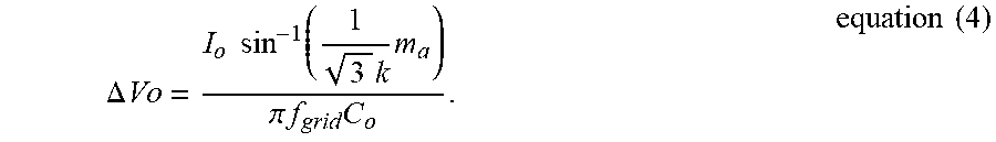
[0045] Neglecting the energy delivered from the primary side to the secondary side during the voltage turn-off time T.sub.off, because very limited energy can be delivered from the primary side to the secondary side during T.sub.off, the voltage drop .DELTA.V.sub.o during T.sub.off can be derived by equation (4) as follows:
.DELTA. Vo = I o sin - 1 ( 1 3 k m a ) .pi. f grid C o . equation ( 4 ) ##EQU00003##
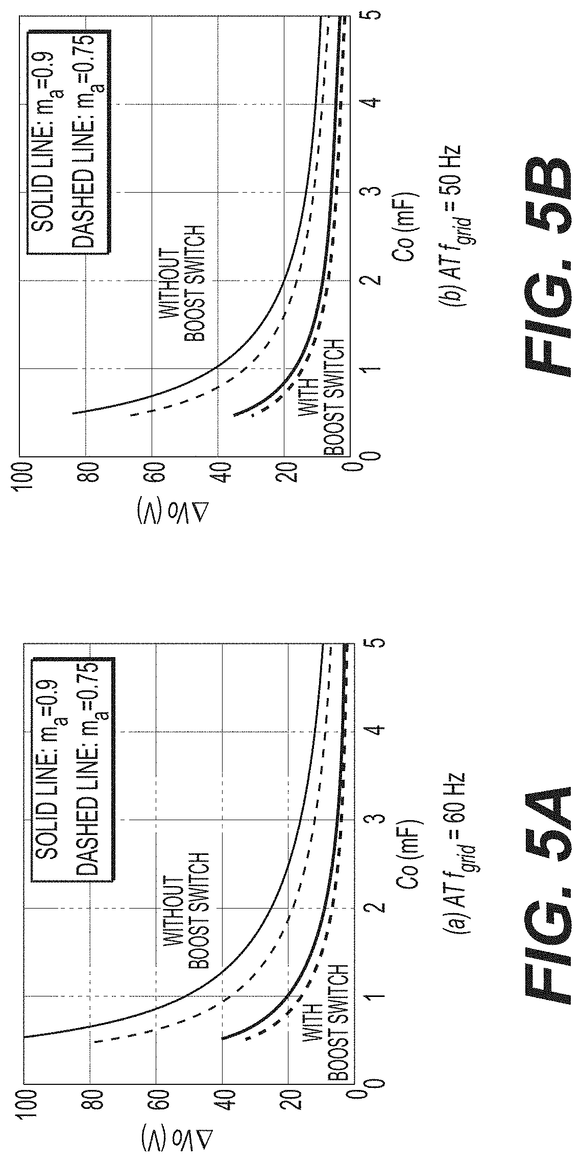
[0046] FIGS. 5A and 5B are graphs comparing an output voltage drop in one-phase-loss operation with a boost switch according to a preferred embodiment of the present invention to an output voltage drop in one-phase-loss operation without a boost switch.
[0047] FIGS. 5A and 5B compare the output voltage drop .DELTA.v.sub.o versus the value of capacitor C.sub.o for the matrix rectifier circuit shown in FIG. 2 with and without boost switch operation. Both cases are plotted at the nominal conditions v.sub.LL=480 V and v.sub.LL=400 V where m.sub.a=0.75 and m.sub.a=0.9 respectively. Both FIGS. 5A and 5B are at the same conditions of l.sub.o=2/3 l.sub.rated and k=1.4.
[0048] Compared with buck operation, the output voltage drop .DELTA.v.sub.o with the boost switch S.sub.boost is significantly lower. According to another preferred embodiment of the present invention, the output capacitance is significantly reduced with boost mode operation if the output voltage drop is kept the same or substantially the same as that of without boost operation. The m.sub.a and grid frequency f.sub.grid also play very important roles in determining the output voltage drop .DELTA.V.sub.o. Either a higher m.sub.a or a lower grid frequency f.sub.grid increases the output voltage drop .DELTA.v.sub.o according to equation (4).
[0049] Because the boost capability is achieved by only adding a boost switch Sboost, a reduction of the power density of the matrix rectifier is very small. In addition, the boost switch S.sub.boost only operates during a relatively small time frame indicated by the shaded intervals in FIGS. 4(c) and 4(d), when |v'.sub.AB| is lower than the output voltage V.sub.o. Therefore, the high current through the boost switch S.sub.boost does not impart a high thermal stress on the boost switch Sboost.
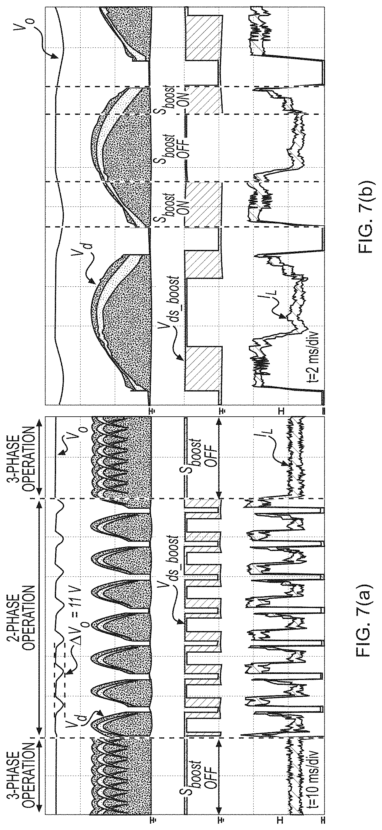
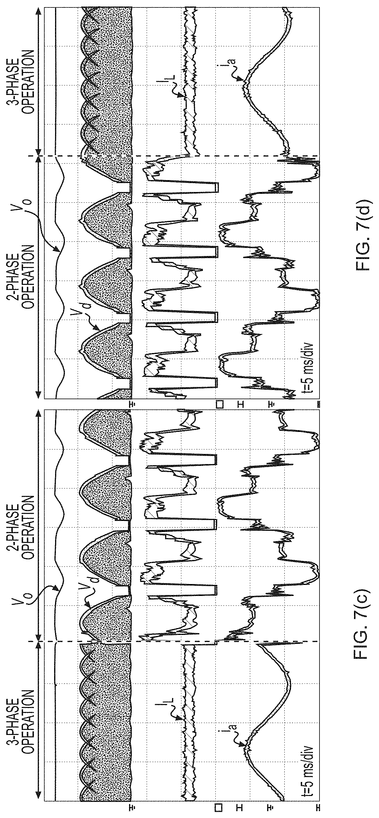
[0050] FIGS. 6(a)-6(e) are graphs showing simulated waveforms of voltage and current characteristics over time of a three-phase rectifier with a boost switch when one phase is shorted and then recovered, according to a preferred embodiment of the present invention. FIGS. 7(a)-7(d) are graphs showing experimental waveforms of a three-phase rectifier with a boost switch both during three-phase operation and during two-phase operation, according to a preferred embodiment of the present invention.
[0051] Simulation and experimental results of preferred embodiments of the present invention are shown in FIGS. 6(a)-6(e) and FIGS. 7(a)-7(d). The operating conditions for both the simulation and experiment are as follows: the input line-to-line voltage v.sub.LL=480 V (at m.sub.a=0.75), the line frequency f.sub.grid=60 Hz, the output inductor over current ratio k=1.4, and the output storage energy C.sub.o =1.4 mF. In FIGS. 6(a)-6(e), at time t.sub.1, "phase C" is shorted, and at timel t.sub.2, "phase C" is recovered. When DC voltage Vd is higher than the output voltage V.sub.o, the converter operates in buck mode. When the DC voltage V.sub.d is lower than output voltage V.sub.o, the boost switch is enabled, and the converter operates in buck+boost mode. The maximum inductor current l.sub.hd clamp is clamped at 18.5 A by the controller during one-phase-loss operation. At steady state, the average inductor current I.sub.L_avg is around 8.77 A to deliver two-thirds of the rated power. During time period T.sub.off, when the DC voltage V.sub.d is very low, the converter stops operating because very limited power can be transferred to the load, even with maximum inductor current l.sub.clamp. Smooth transitions between the buck+boost mode and the buck mode can be observed from the output inductor current in FIG. 6(e). The experimental results in FIGS. 7(a)-7(d) verify the simulation results in FIGS. 6(a)-6(e).
[0052] As shown in FIGS. 7(a)-7(d), the output voltage ripple .DELTA.V.sub.0 is about 11 V, which is well within 4% of the nominal output voltage 380 V. The waveform of V.sub.ds_boost shows that the boost switch is only enabled when the output voltage of the DC voltage V.sub.d of the bridge rectifier is lower than the output voltage V.sub.o, which significantly reduces thermal stresses applied to the circuit components.
[0053] The above-described features and advantages of the preferred embodiments of the present invention are able to be applied to a number of different applications, including, but not limited to, battery chargers, electric vehicle chargers high-voltage data center applications, telecommunications applications, aerospace applications, and the like.
[0054] While preferred embodiments of the present invention have been described above, it is to be understood that variations and modifications will be apparent to those skilled in the art without departing the scope and spirit of the present invention. The scope of the present invention, therefore, is to be determined solely by the following claims.
* * * * *
D00000
D00001
D00002
D00003
D00004
D00005
D00006
D00007
D00008
XML
uspto.report is an independent third-party trademark research tool that is not affiliated, endorsed, or sponsored by the United States Patent and Trademark Office (USPTO) or any other governmental organization. The information provided by uspto.report is based on publicly available data at the time of writing and is intended for informational purposes only.
While we strive to provide accurate and up-to-date information, we do not guarantee the accuracy, completeness, reliability, or suitability of the information displayed on this site. The use of this site is at your own risk. Any reliance you place on such information is therefore strictly at your own risk.
All official trademark data, including owner information, should be verified by visiting the official USPTO website at www.uspto.gov. This site is not intended to replace professional legal advice and should not be used as a substitute for consulting with a legal professional who is knowledgeable about trademark law.