Light Emitting Device And Manufacturing Method Thereof
CHOI; Sukyung ; et al.
U.S. patent application number 16/839857 was filed with the patent office on 2021-03-04 for light emitting device and manufacturing method thereof. This patent application is currently assigned to ELECTRONICS AND TELECOMMUNICATIONS RESEARCH INSTITUTE. The applicant listed for this patent is ELECTRONICS AND TELECOMMUNICATIONS RESEARCH INSTITUTE. Invention is credited to CHUNWON BYUN, Hyunsu CHO, Nam Sung CHO, Sukyung CHOI, Chan-mo KANG, Byoung-Hwa KWON, Hyunkoo LEE, Jaehyun MOON, Jin Wook SHIN.
| Application Number | 20210066631 16/839857 |
| Document ID | / |
| Family ID | 1000004886670 |
| Filed Date | 2021-03-04 |


View All Diagrams
| United States Patent Application | 20210066631 |
| Kind Code | A1 |
| CHOI; Sukyung ; et al. | March 4, 2021 |
LIGHT EMITTING DEVICE AND MANUFACTURING METHOD THEREOF
Abstract
Provided is a light emitting device including a lower electrode, an upper electrode disposed to face the lower electrode, a quantum dot light emitting layer between the lower electrode and the upper electrode, an electron transport layer between the lower electrode and the quantum dot light emitting layer, and a hole transport layer between the upper electrode and the quantum dot light emitting layer, wherein the quantum dot light emitting layer includes a quantum dot, and a first ligand on a surface of the quantum dot, and a second ligand on the surface of the quantum dot.
| Inventors: | CHOI; Sukyung; (Daejeon, KR) ; LEE; Hyunkoo; (Daejeon, KR) ; KWON; Byoung-Hwa; (Daejeon, KR) ; MOON; Jaehyun; (Daejeon, KR) ; CHO; Hyunsu; (Daejeon, KR) ; KANG; Chan-mo; (Daejeon, KR) ; BYUN; CHUNWON; (Daejeon, KR) ; SHIN; Jin Wook; (Daejeon, KR) ; CHO; Nam Sung; (Daejeon, KR) | ||||||||||
| Applicant: |
|
||||||||||
|---|---|---|---|---|---|---|---|---|---|---|---|
| Assignee: | ELECTRONICS AND TELECOMMUNICATIONS
RESEARCH INSTITUTE Daejeon KR |
||||||||||
| Family ID: | 1000004886670 | ||||||||||
| Appl. No.: | 16/839857 | ||||||||||
| Filed: | April 3, 2020 |
| Current U.S. Class: | 1/1 |
| Current CPC Class: | H01L 51/0061 20130101; H01L 51/56 20130101; C09K 2211/1029 20130101; H01L 51/5072 20130101; C09K 11/06 20130101; H01L 51/502 20130101; H01L 2251/303 20130101; H01L 51/5056 20130101; H01L 51/0072 20130101; H01L 51/0003 20130101; H01L 51/0037 20130101; H01L 51/0035 20130101 |
| International Class: | H01L 51/50 20060101 H01L051/50; H01L 51/00 20060101 H01L051/00; H01L 51/56 20060101 H01L051/56; C09K 11/06 20060101 C09K011/06 |
Foreign Application Data
| Date | Code | Application Number |
|---|---|---|
| Aug 29, 2019 | KR | 10-2019-0106369 |
Claims
1. A light emitting device, comprising: a lower electrode; an upper electrode disposed to face the lower electrode; a quantum dot light emitting layer between the lower electrode and the upper electrode; an electron transport layer between the lower electrode and the quantum dot light emitting layer; and a hole transport layer between the upper electrode and the quantum dot light emitting layer, wherein the quantum dot light emitting layer comprises a quantum dot, a first ligand on a surface of the quantum dot, and a second ligand on the surface of the quantum dot, the first ligand is adjacent to the electron transport layer, the first ligand is an organic compound having a chain structure, the second ligand is adjacent to the hole transport layer, the second ligand is an organic compound having a ring structure, and a length of the second ligand is shorter than a length of the first ligand.
2. The light emitting device of claim 1, wherein the second ligand is pyridine.
3. The light emitting device of claim 1, wherein the quantum dot light emitting layer has a multilayer structure in which quantum dots are stacked.
4. The light emitting device of claim 1, wherein the second ligand is disposed at an interface between the quantum dot light emitting layer and the hole transport layer.
5. The light emitting device of claim 1, wherein the quantum dot comprises Group II-VI, Group III-V, or Group I-III-VI nano-semiconductor compounds.
6. The light emitting device of claim 1, wherein the quantum dot comprises cadmium selenide (CdSe), cadmium sulfide (CdS), cadmium telluride (CdTe), zinc sulfide (ZnS), zinc selenide (ZnSe), zinc telluride (ZnTe), indium phosphide (InP), indium arsenide (InAs), copper indium sulfide (CuInS.sub.2), copper indium selenide (CuInSe.sub.2), or a mixture thereof.
7. The light emitting device of claim 1, wherein the electron transport layer comprises zinc oxide (ZnO), titanium dioxide (TiO.sub.2), tungsten trioxide (WO.sub.3), or a mixture thereof.
8. The light emitting device of claim 1, wherein the hole transport layer comprises poly(9,9-dioctylfluorene-alt-N-(4-sec-butylphenyl)-diphenylamin- e) (TFB), 4,4',4''-tris(carbazol-9-yl)triphenylamine (TCTA), N,N'-di(1-naphthyl)-N,N'-diphenyl-(1,1'-biphenyl)-4,4'-diamine (NPB), poly[N,N'-bis(4-butylphenyl)-N,N'-bisphenylbenzidine] (Poly-TPD), 4,4'-bis (9-carbazolyl)-1,1'-biphenyl (CBP), or a mixture thereof.
9. The light emitting device of claim 1, comprising a hole injection layer between the hole transport layer and the upper electrode, wherein the hole injection layer comprises MoO.sub.3, poly(3,4-ethylenedioxythiophene):polystyrene sulfonate (PEDOT:PSS), or a mixture thereof.
10. A method for manufacturing a light emitting device, the method comprising: forming an electron transport layer on a lower electrode; synthesizing a quantum dot a surface of which first ligands bind to; providing the synthesized quantum dot on the electron transport layer to form a quantum dot emitting layer; substituting at least one of the first ligands of the quantum dot of the quantum dot light emitting layer with a second ligand; forming a hole transport layer on the quantum dot light emitting layer; and forming an upper electrode on the hole transport layer.
11. The method of claim 10, further comprising forming a hole injection layer between the hole transport layer and the upper electrode.
12. The method of claim 10, wherein: each of the first ligands is an organic compound having a chain structure; the second ligand is an organic compound having a ring structure; and a length of the second ligand is shorter than a length of the first ligand.
13. The method of claim 10, wherein the second ligand is pyridine.
14. The method of claim 10, wherein the quantum dot light emitting layer has a multilayer structure in which quantum dots are stacked.
15. The method of claim 10, wherein the second ligand is disposed at an interface between the quantum dot light emitting layer and the hole transport layer.
16. The method of claim 10, wherein the substituting at least one of the first ligands of the quantum dot of the quantum dot light emitting layer with the second ligand is performed through a spin coating process, a spray coating process, a bar coating process or a dipping process.
Description
CROSS-REFERENCE TO RELATED APPLICATIONS
[0001] This U.S. non-provisional patent application claims priority under 35 U.S.C. .sctn. 119 of Korean Patent Application No. 10-2019-0106369, filed on Aug. 29, 2019, the entire contents of which are hereby incorporated by reference.
BACKGROUND
[0002] The present disclosure herein relates to a light emitting device and a manufacturing method thereof.
[0003] Recently, there is a growing demand for a high color reproduction display capable of faithfully reproducing colors close to nature. Thus, interest in quantum dot light emitting devices as a next generation display device having good color reproducibility is increasing.
[0004] A quantum dot light emitting device refers to a device which emits light by itself upon combination of electrons and holes injected from both electrodes of a light emitting layer including quantum dots. In order to secure the performance and sufficient lifetime of the light emitting device, the electrons and holes in the light emitting layer should be balanced. However, although electrons are readily movable inside the light emitting device, holes having a large energy level difference unlike electrons may not be readily injected into the light emitting layer, thereby causing an electron-hole imbalance issue in the light emitting layer. Accordingly, researches to solve such an electron-hole imbalance phenomenon in the light emitting layer have been actively conducted.
SUMMARY
[0005] The present disclosure provides a quantum dot light emitting device having an improved electron-hole imbalance phenomenon.
[0006] The present disclosure also provides a method for manufacturing a quantum dot light emitting device having an improved electron-hole imbalance phenomenon.
[0007] An embodiment of the inventive concept provides a quantum dot light emitting device including a lower electrode, an upper electrode disposed to face the lower electrode, a quantum dot light emitting layer between the lower electrode and the upper electrode, an electron transport layer between the lower electrode and the quantum dot light emitting layer, and a hole transport layer between the upper electrode and the quantum dot light emitting layer, wherein the quantum dot light emitting layer includes a quantum dot, and a first ligand on a surface of the quantum dot, and a second ligand on the surface of the quantum dot, the first ligand is adjacent to the electron transport layer, the first ligand is an organic compound having a chain structure, the second ligand is adjacent to the hole transport layer, the second ligand is an organic compound having a ring structure, and a length of the second ligand may be shorter than a length of the first ligand.
[0008] In an embodiment, the second ligand may be pyridine.
[0009] In an embodiment, the quantum dot light emitting layer may have a multilayer structure in which quantum dots are stacked.
[0010] In an embodiment, the second ligand may be disposed at an interface between the quantum dot light emitting layer and the hole transport layer.
[0011] In an embodiment, the quantum dot may include Group II-VI, Group III-V, or Group I-III-VI nano-semiconductor compounds.
[0012] In an embodiment, the quantum dot may include cadmium selenide (CdSe), cadmium sulfide (CdS), cadmium telluride (CdTe), zinc sulfide (ZnS), zinc selenide (ZnSe), zinc telluride (ZnTe), indium phosphide (InP), indium arsenide (InAs), copper indium sulfide (CuInS.sub.2), copper indium selenide (CuInSe.sub.2), or a mixture thereof.
[0013] In an embodiment, the electron transport layer may include zinc oxide (ZnO), titanium dioxide (TiO.sub.2), tungsten trioxide (WO.sub.3), or a mixture thereof.
[0014] In an embodiment, the hole transport layer may include poly(9,9-dioctylfluorene-alt-N-(4-sec-butylphenyl)-diphenylamine) (TFB), 4,4',4''-tris(carbazol-9-yl)triphenylamine (TCTA), N,N'-di(1-naphthyl)-N,N'-diphenyl-(1,1'-biphenyl)-4,4'-diamine (NPB), poly[N,N'-bis(4-butylphenyl)-N,N'-bisphenylbenzidine](Poly-TPD), 4,4'-bis (9-carbazolyl)-1,1'-biphenyl (CBP), or a mixture thereof.
[0015] In an embodiment, a hole injection layer between the hole transport layer and the upper electrode is included, and the hole injection layer may include MoO.sub.3, poly(3,4-ethylenedioxythiophene):polystyrene sulfonate (PEDOT:PSS), or a mixture thereof.
[0016] In an embodiment of the inventive concept, a method for manufacturing a light emitting device includes forming an electron transport layer on a lower electrode, synthesizing a quantum dot a surface of which first ligands bind to, providing the synthesized quantum dot on the electron transport layer to form a quantum dot emitting layer, substituting at least one of the first ligands of the quantum dot of the quantum dot light emitting layer with a second ligand, forming a hole transport layer on the quantum dot light emitting layer, and forming an upper electrode on the hole transport layer.
[0017] In an embodiment, forming a hole injection layer between the hole transport layer and the upper electrode may be further included.
[0018] In an embodiment, each of the first ligands is an organic compound having a chain structure, the second ligand is an organic compound having a ring structure, and a length of the second ligand may be shorter than a length of the first ligand.
[0019] In an embodiment, the second ligand may be pyridine.
[0020] In an embodiment, the quantum dot light emitting layer may have a multilayer structure in which quantum dots are stacked.
[0021] In an embodiment, the second ligand may be disposed at an interface between the quantum dot light emitting layer and the hole transport layer.
[0022] In an embodiment, the substituting at least one of the first ligands of the quantum dot of the quantum dot light emitting layer with the second ligand may be performed through a spin coating process, a spray coating process, a bar coating process or a dipping process.
BRIEF DESCRIPTION OF THE FIGURES
[0023] The accompanying drawings are included to provide a further understanding of the inventive concept, and are incorporated in and constitute a part of this specification. The drawings illustrate exemplary embodiments of the inventive concept and, together with the description, serve to explain principles of the inventive concept. In the drawings:
[0024] FIG. 1 is a cross-sectional view of a quantum dot light emitting device according to embodiments of the inventive concept;
[0025] FIGS. 2A to 2C are conceptual views illustrating a quantum dots according to embodiments of the inventive concept;
[0026] FIGS. 3A to 3C are cross-sectional views of quantum dot light emitting devices according to embodiments of the inventive concept;
[0027] FIGS. 4A and 4B show images obtained by observing cross sections of quantum dot light emitting devices manufactured according to Example and Comparative Example using a transmission electron microscope.
[0028] FIG. 5 is a view illustrating an energy level of a quantum dot light emitting device according to embodiments of the inventive concept;
[0029] FIG. 6 is a graph showing the transmittances in the infrared region of quantum dot light emitting devices manufactured according to Example and Comparative Example;
[0030] FIGS. 7A to 7C are graphs showing absorption spectra in the ultraviolet-visible light region of quantum dot light emitting devices manufactured according to Example and Comparative Example;
[0031] FIGS. 8A to 8F are graphs showing current density, luminance, current efficiency, and power efficiency of quantum dot light emitting devices manufactured according to Example and Comparative Example;
[0032] FIG. 9 shows comparison results of brightness of quantum dot light emitting devices manufactured according to Example and Comparative Example;
[0033] FIG. 10 is a graph showing electroluminescence spectra of quantum dot light emitting devices manufactured according to Example and Comparative Example; and
[0034] FIG. 11 shows color coordinates of a quantum dot light emitting device manufactured according to an embodiment.
DETAILED DESCRIPTION
[0035] In order to help fully understand the configuration and effects of the present disclosure, preferred embodiments of the present disclosure will be explained with reference to the accompanying drawings. However, the present disclosure should not be construed as limited to the embodiments set forth herein and may be embodied in different forms and various changes can be made. These embodiments are provided so that this disclosure will be thorough and complete, and will fully convey the scope of the invention to those skilled in the art.
[0036] In the specification, it will be understood that when an element is referred to as being "on" another element, it can be directly on the other element or intervening elements may be present. Also, in the drawings, the thickness of elements is exaggerated for an effective description of technical contents. Like numbers refer to like elements throughout.
[0037] It will be understood that, although the terms "first", "second", etc. may be used herein to describe various elements, these elements should not be limited by these terms. These terms are only used to distinguish one element from another. Embodiments described and exemplified herein include complementary embodiments thereof.
[0038] The terms used in the present disclosure are for explaining the exemplary embodiments rather than limiting the present disclosure. Unless particularly stated otherwise in the present specification, a singular form also includes a plural form. The meaning of "comprises" and/or "comprising" used in this specification does not exclude the existence or addition of one or more other elements in addition to the mentioned elements.
[0039] FIG. 1 is a cross-sectional view of a quantum dot light emitting device 10 according to embodiments of the inventive concept.
[0040] Referring to FIG. 1, a quantum dot light emitting device 10 including a lower electrode 100, an electron transport layer 200, a quantum dot light emitting layer 300, a hole transport layer 400, a hole injection layer 500, and an upper electrode 600 may be provided.
[0041] The lower electrode 100 may be provided on a substrate (not shown) and may include a transparent conductive material. For example, the lower electrode 100 may include a transparent conductive oxide (TCO) thin film (e.g., an indium tin oxide (ITO) thin film or an indium zinc oxide (IZO) thin film), a conductive organic thin film (e.g., a thin film including at least one of copper iodide, polyaniline, poly(3-methylthiophene), or pyrrole), or a graphene thin film. In exemplary embodiments, the lower electrode 100 may be formed by a thermal deposition process, a chemical vapor deposition (CVD) process, or an atomic layer deposition (ALD) process.
[0042] The electron transport layer 200 may be formed on the lower electrode 100. The electron transport layer 200 may stably supply electrons to the quantum dot light emitting layer 300. The electron transport layer 200 may include a material having high electron mobility, and may include, for example, zinc oxide (ZnO), titanium dioxide (TiO.sub.2), tungsten trioxide (WO.sub.3), or a mixture thereof.
[0043] The quantum dot light emitting layer 300 may be formed on the electron transport layer 200. The quantum dot light emitting layer 300 is a light emitting layer including quantum dots QD, and electrons and holes injected from both electrodes may combine to generate light. The quantum dot light emitting layer 300 may generate light of a first color, a second color, a third color, or white color, and for example, the first to third colors may be red, green, and blue.
[0044] The quantum dot light emitting layer 300 may include nano-sized quantum dots QD having a diameter of about 1 to about 100 nm, and for example, the quantum dots QD may include Group II-VI, Group III-V, or Group I-III-VI nano-semiconductor compounds. For example, the quantum dots QD may include cadmium selenide (CdSe), cadmium sulfide (CdS), cadmium telluride (CdTe), zinc sulfide (ZnS), zinc selenide (ZnSe), zinc telluride (ZnTe), indium phosphide (InP), indium arsenide (InAs), copper indium sulfide (CuInS.sub.2), copper indium selenide (CuInSe.sub.2), or a mixture thereof.
[0045] The quantum dot QD according to an embodiment of the inventive concept may be synthesized by heating a precursor solution in a vacuum state. The precursor solution may include a first precursor solution and a second precursor solution. For example, the first precursor solution may be a Cd precursor solution and the second precursor solution may be a Se precursor solution. The first precursor solution and the second precursor solution may react with each other to generate CdSe quantum dots. As another example, the first precursor solution may be a Cd precursor solution and the second precursor solution may be a S precursor solution. The first precursor solution and the second precursor solution may react with each other to generate CdS quantum dots.
[0046] The synthesis temperature of the quantum dot QD is not particularly limited, but may be, for example, about 90.degree. C. to about 350.degree. C.
[0047] The precursor solution may further include an organic compound capable of providing a ligand on the surface of the quantum dot QD. While the quantum dot is formed, the organic compound may bind to the surface of the quantum dot as its surface ligand. The type of the organic compound is not particularly limited, and may include, for example, oleic acid, trioctylphosphine, trioctylphosphine-oxide, oleylamine or a mixture thereof. Residual organic compounds that do not bind to the quantum dots QD may be removed using an anti-solvent. The anti-solvent may include methanol or acetone.
[0048] The quantum dots QD may be coated on the electron transport layer 200 through a solution process, and the ligand may bind to the surface of the quantum dot QD to uniformly disperse the quantum dots QD in a solvent used in the solution process. The ligand binding to the surface of the quantum dot QD may have a functional group, and the functional group may have a specific charge. Electrical attraction or repulsion generated by the ligand having a charged functional group may affect the charge mobility and energy level of the quantum dot light emitting layer 300.
[0049] The hole transport layer 400 may be formed on the quantum dot light emitting layer 300. The hole transport layer 400 may provide holes to the quantum dot light emitting layer 300. For example, the hole transport layer 400 may include poly(9,9-dioctylfluorene-alt-N-(4-sec-butylphenyl)-diphenylamine) (TFB), 4,4', 4''-tris(carbazol-9-yl)triphenylamine (TCTA), N,N'-Di(1-naphthyl)-N, N'-diphenyl-(1,1'-biphenyl)-4,4'-diamine (NPB), poly[N,N'-bis(4-butylphenyl)-N,N'-bisphenylbenzidine] (Poly-TPD), 4,4'-bis(9-carbazolyl)-1,1'-biphenyl (CBP), or a mixture thereof.
[0050] The hole injection layer 500 may be formed on an upper part of the hole transport layer 400. The hole injection layer 500 may facilitate the hole injection into the hole transport layer 400 to reduce the driving current and the driving voltage of the light emitting device. For example, the hole injection layer 500 may include MoO.sub.3, poly(3,4-ethylenedioxythiophene) polystyrene sulfonate (PEDOT:PSS), or a mixture thereof.
[0051] The upper electrode 600 may be formed on the hole injection layer 500. The upper electrode 600 may include a conductive material having a lower work function than the lower electrode 100. For example, the upper electrode 600 may include aluminum (Al), gold (Au), silver (Ag), iridium (Ir), molybdenum (Mo), palladium (Pd), platinum (Pt), or a combination thereof. In exemplary embodiments, the upper electrode 600 may be formed by a deposition process. In exemplary embodiments, the upper electrode 600 may be formed by a thermal evaporation process, a chemical vapor deposition process, or an atomic layer deposition process.
[0052] FIGS. 2A to 2C are conceptual views illustrating a quantum dot QD according to embodiments of the inventive concept.
[0053] Referring to FIG. 2A, at least one first ligand LG1 may bind to the surface of the quantum dot QD. The first ligand LG1 may be an organic compound having a chain structure, and may include, for example, oleic acid, trioctylphosphine, trioctylphosphine oxide, oleylamine or a mixture thereof.
[0054] Referring to FIG. 2B, at least one first ligand LG1 and at least one second ligand LG2 may bind to the surface of the quantum dot QD. The first ligand LG1 and the second ligand LG2 may have different structures from each other. The length of the second ligand LG2 may be shorter than the length of the first ligand LG1. For example, each of the first ligand LG1 and the second ligand LG2 may be an organic compound having a chain structure. The chain length of the second ligand LG2 may be shorter than the chain length of the first ligand LG1.
[0055] Referring to FIG. 2C, at least one first ligand LG1 and at least one second ligand LG2 may bind to the surface of the quantum dot QD. The first ligand LG1 and the second ligand LG2 may have different structures from each other. The length of the second ligand LG2 may be shorter than the length of the first ligand LG1. For example, the first ligand LG1 may be an organic compound having a chain structure, and the second ligand LG2 may be an organic compound having a ring structure. For example, the second ligand LG2 may include pyridine.
[0056] FIGS. 3A to 3C are cross-sectional views illustrating quantum dot light emitting devices according to embodiments of the inventive concept. Hereinafter, duplicate descriptions as those described with reference to FIGS. 2A to 2C will be omitted.
[0057] Referring to FIGS. 3A to 3C, the quantum dot light emitting layer 300 may have a multilayer structure in which quantum dots QD are stacked. As illustrated in FIGS. 3A to 3C, the quantum dot light emitting layer 300 may have a layered structure in which a first quantum dot layer 301 and a second quantum dot layer 302 are stacked in order on the electron transport layer 200.
[0058] As illustrated in FIG. 3B or 3C, at least one of the first ligands LG1 binding to the surface of the quantum dot QD may be substituted with a second ligand LG2 having a different structure from that of the first ligand LG1. As illustrated in FIG. 3B, at least one of the first ligands LG1 binding to the surface of the second quantum dot layer 302 may be substituted with the second ligand LG2, and the length of the second ligand LG2 may be shorter than the length of the first ligand LG1. As illustrated in FIG. 3C, at least one of the first ligands LG1 binding to the surface of the second quantum dot layer 302 may be substituted with the second ligand LG2, and the second ligand LG2 may be pyridine. The substitution process is not particularly limited, and may be performed through, for example, a spin coating process, a spray coating process, a bar coating process or a dipping process.
[0059] The first ligand LG1 binding to the first quantum dot layer 301 is adjacent to the electron transport layer 200, and the second ligand LG2 binding to the second quantum dot layer 302 may be adjacent to a hole transport layer (see a hole transport layer 400 of FIG. 1). When the length of the second ligand LG2 adjacent to the hole transport layer is shorter than the length of the first ligand LG1 adjacent to the electron transport layer 200, the hole transfer from the hole transport layer to the quantum dot light emitting layer 300 may be readily performed. As a result, the hole-electron imbalance phenomenon in the quantum dot light emitting layer 300 may be alleviated. The second ligand LG2 may be disposed at an interface between the quantum dot light emitting layer 300 and the hole transport layer.
Example--Manufacture of Quantum Dot Light Emitting Devices
[0060] In an embodiment of the inventive concept, a quantum dot light emitting device corresponding to a visible light region was manufactured using cadmium (Cd)-based red, green, and blue light emitting quantum dots. Indium tin oxide (ITO) was deposited and patterned on a glass substrate to form a negative electrode, and an electron transport layer was formed on the negative electrode through spin coating using zinc oxide (ZnO) nanoparticles. A light emitting layer was formed on the electron transport layer by spin coating using a quantum dot solution. In terms of the quantum dot solution, the quantum dot particles contained organic ligands (oleic acid and trioctylphosphine) at the time of synthesis, were thus used by being dispersed in an organic solvent (toluene and octane).
[0061] After forming the quantum dot light emitting layer, the pyridine solution was dropped onto the quantum dot light emitting layer in order to substitute a ligand on the quantum dot light emitting layer, and then the existing ligand exposed to the upper end of the quantum dot was substituted with pyridine through spin coating. After the pyridine solution treatment, methanol was used to remove the substituted ligand and the unsubstituted pyridine. As a result, a quantum dot light emitting layer in which only the upper part of the quantum dot light emitting layer was selectively substituted with a pyridine ligand was manufactured. Thereafter, a hole transport layer (TCTA), a hole injection layer (MoO.sub.3), and an upper electrode (Ag) were deposited on the quantum dot light emitting layer in order through a thermal evaporation process to manufacture a quantum dot light emitting device at the end.
Comparative Example--Manufacture of Quantum Dot Light Emitting Devices
[0062] A quantum dot light emitting device according to Comparative Example was manufactured in the same manner as the manufacturing method of the quantum dot light emitting device in Example above. However, the step of substituting a ligand on the quantum dot light emitting layer with pyridine was not performed.
[0063] FIGS. 4A and 4B show images obtained by observing cross sections of quantum dot light emitting devices manufactured according to Example and Comparative Example respectively, using a transmission electron microscope.
[0064] FIG. 5 is a view illustrating an energy level of a quantum dot light emitting device manufactured according to an embodiment. It could be confirmed that when the surface of the quantum dot QD includes pyridine as a second ligand LG2 (see FIG. 2C), the highest occupied molecular orbital (HOMO) level of the pyridine is positioned halfway between the valence band of the quantum dot and the HOMO level of TCTA to generate a cascade energy form. The result indicates that the substituted short pyridine ligand not only reduces the distance between the quantum dot light emitting layer and the hole transport layer, but also forms an intermediate energy level between the quantum dot and the hole transport layer so that holes are readily transferred, thereby improving the inefficient hole injection issue in the quantum dot light emitting device.
Experimental Example 1--Observation of Optical Properties Changes of Quantum Dots According to Example and Comparative Example
[0065] The optical properties of the quantum dot in the quantum dot light emitting devices manufactured according to Example and Comparative Example were observed. The transmittance in the infrared region was measured.
[0066] FIG. 6 is a graph showing the results obtained by measuring the transmittance in the infrared region of the quantum dot light emitting devices manufactured according to Example and Comparative Example using a Fourier transform infrared (FTIR) spectroscope. As illustrated in FIG. 6, in the quantum dot in the quantum dot light emitting device manufactured according to the Comparative Example, C.dbd.N stretch peak (1731 cm.sup.-1) due to pyridine was not observed in the spectrum. On the other hand, the C.dbd.N stretch peak (1731 cm.sup.-1) was observed in the quantum dot light emitting device manufactured according to the Example to demonstrate that pyridine exists on the surface of the quantum dot.
[0067] FIGS. 7A to 7C are graphs showing an absorption spectrum in the ultraviolet-visible light region of quantum dot light emitting devices manufactured according to Example and Comparative Example. As illustrated in FIGS. 7A to 7C, it could be confirmed that red, green, and blue quantum dots RQD/pyridine, GQD/pyridine, and BQD/pyridine substituted with pyridine maintain the inherent absorbance characteristics of the quantum dots.
Experimental Example 2--Evaluation of Luminance, Current Efficiency, and Power Efficiency of Quantum Dot Light Emitting Devices According to Example and Comparative Example
[0068] In order to examine the effects of the quantum dot light emitting device manufactured according to the inventive concept, the current density, luminance, current efficiency, and power efficiency of the quantum dot light emitting devices manufactured according to Example and Comparative Example were compared and analyzed.
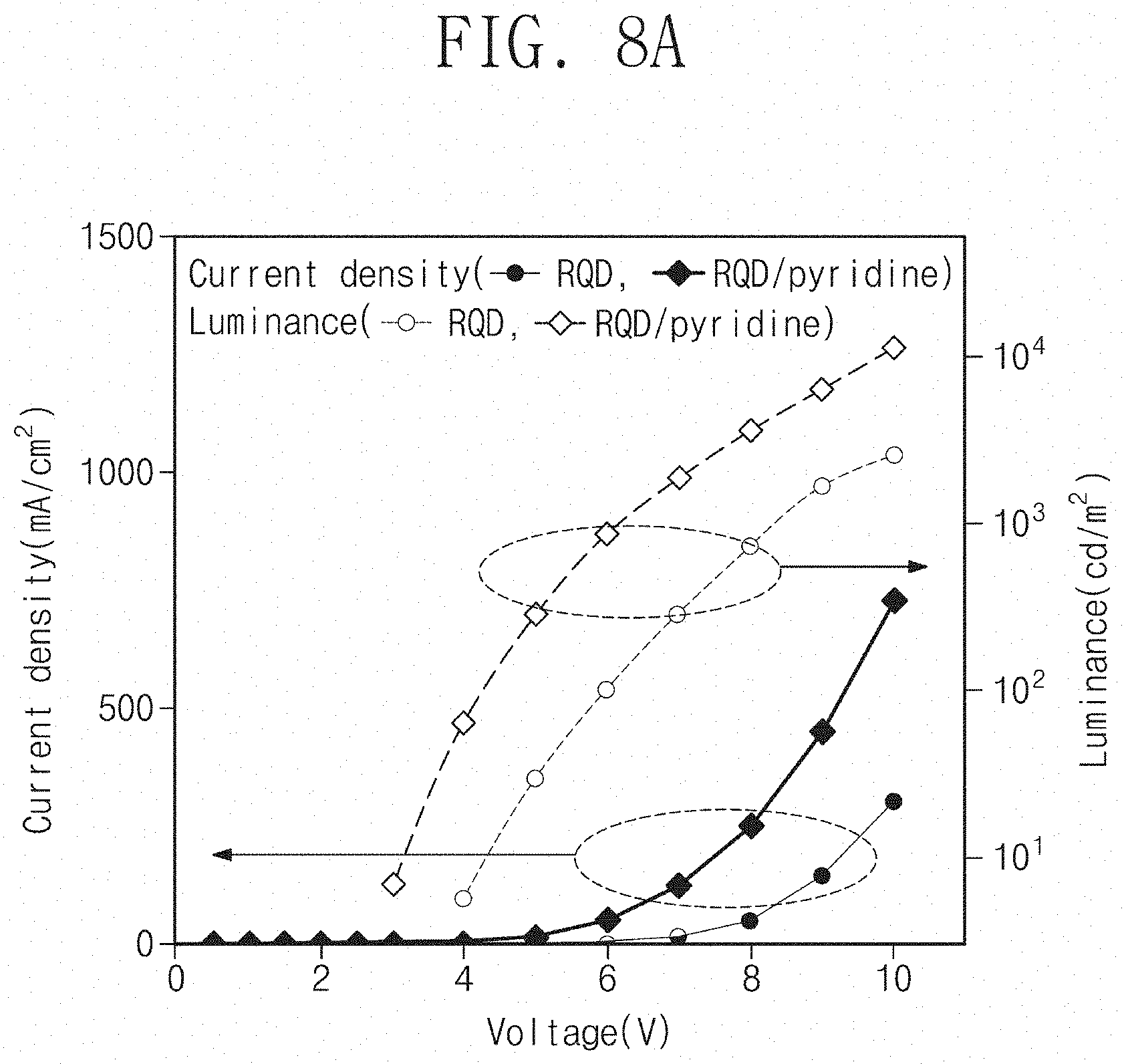
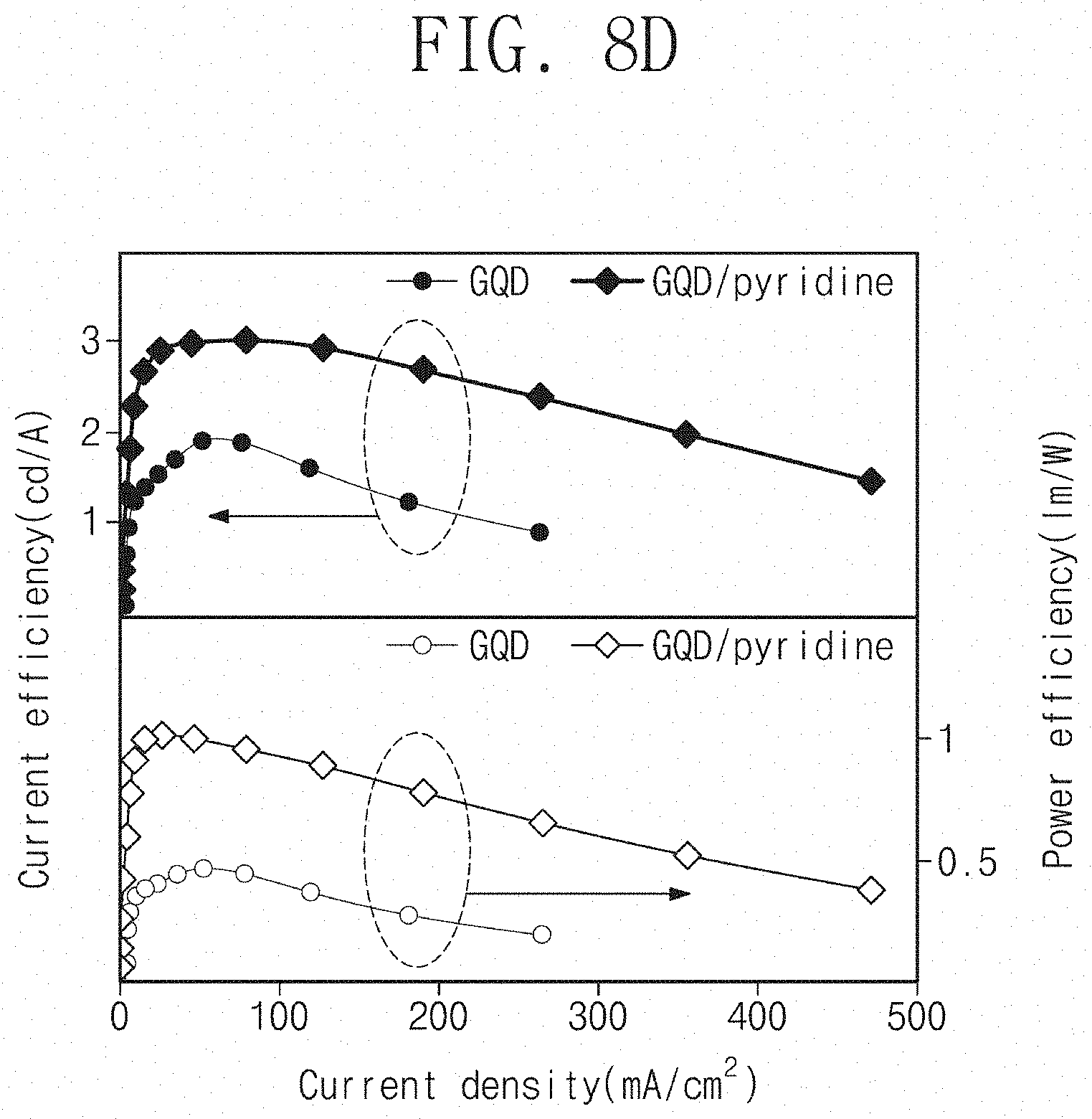
[0069] FIGS. 8A to 8F are graphs showing measurement results of current density, luminance, current efficiency, and power efficiency of red, green, and blue quantum dots manufactured according to Example and Comparative Example.
[0070] As illustrated in FIGS. 8A, 8C, and 8E, in red, green, and blue quantum dot light emitting devices (RQD/pyridine, GQD/pyridine, and BQD/pyridine) manufactured according to Example, it could be confirmed that turn-on voltage was pulled, and the luminance also increased compared to the red, green, and blue quantum dot light emitting devices RQD, GQD, and BQD manufactured according to Comparative Example.
[0071] As illustrated in FIGS. 8B, 8D, and 8F, when observing the current efficiency and power efficiency of the quantum dot light emitting devices, it could be confirmed that the current efficiency and power efficiency of the red, green, and blue quantum dot light emitting devices (RQD/pyridine, GQD/pyridine, and BQD/pyridine) manufactured according to the Example were superior to those of the red, green, and blue quantum dot light emitting devices (RQD, GQD, and BQD) manufactured according to the Comparative Example. As a result, it could be confirmed that regardless of the emission color and the quantum dot energy level, the quantum dot substituted with pyridine manufactured according to the Example facilitates the hole movement in the quantum dot light emitting device, thereby improving the performance of the quantum dot light emitting device.
Experimental Example 3--Evaluation of Brightness, Electroluminescence (EL) Spectrum and Color Coordinates of Quantum Dot Light Emitting Devices According to Example and Comparative Example
[0072] In order to examine the effects of the quantum dot light emitting devices manufactured according to the inventive concept, the brightness and EL spectrum of the quantum dot light emitting devices manufactured according to Example and Comparative Example were compared and the color coordinates were evaluated.
[0073] As illustrated in FIG. 9, it is confirmed that the red, green, and blue quantum dot light emitting devices (RQD/pyridine, GQD/pyridine, and BQD/pyridine) manufactured according to Example emit much brighter light than the red, green, and blue quantum dot light emitting didoes (RQD, GQD, and BQD) manufactured according to Comparative Example under the same voltage.
[0074] As illustrated in FIG. 10, when comparing the electroluminescence (EL) spectrum of red, green, and blue quantum dot light emitting devices (RQD/pyridine, GQD/pyridine, and BQD/pyridine) manufactured according to Example and red, green, and blue quantum dot light emitting devices (RQD, GQD, and BQD) manufactured according to Comparative Example, it could be confirmed that even if the surface of the quantum dot was substituted with pyridine, the emission characteristic of the quantum dot itself was not affected and full width at half maximum (FWHM) was maintained.
[0075] In addition, as illustrated in FIG. 11, as a result of evaluating the color coordinates of the quantum dot light emitting devices manufactured according to Example indicate that the quantum dot light emitting devices are suitable as a high color reproduction light emitting device since a quite large area of 159% of NTSC1987 and 78% of BT2020 is covered.
[0076] In a quantum dot light emitting device according to an embodiment of the inventive concept, transferring holes from a hole transport layer to a quantum dot light emitting layer may be readily performed by controlling a ligand on the surface of a quantum dot. Therefore, the electron-hole imbalance phenomenon in the quantum dot light emitting layer may be improved. In addition, the quantum dot light emitting device according to an embodiment of the inventive concept may have improved brightness, current efficiency, and power efficiency.
[0077] However, the effects of embodiments of the inventive concept are not limited to the above disclosure.
[0078] Although the exemplary embodiments of the present disclosure have been described with reference to the accompanying drawings, it will be understood to those skilled in the art that the present invention may be implemented in different specific forms without changing the technical ideals or essential features. Accordingly, it should be understood that the embodiments described herein are illustrative not restrictive in all aspects.
* * * * *
D00000
D00001
D00002
D00003
D00004
D00005
D00006
D00007
D00008
D00009
D00010
D00011
D00012

D00013
D00014

D00015

D00016

D00017

D00018

XML
uspto.report is an independent third-party trademark research tool that is not affiliated, endorsed, or sponsored by the United States Patent and Trademark Office (USPTO) or any other governmental organization. The information provided by uspto.report is based on publicly available data at the time of writing and is intended for informational purposes only.
While we strive to provide accurate and up-to-date information, we do not guarantee the accuracy, completeness, reliability, or suitability of the information displayed on this site. The use of this site is at your own risk. Any reliance you place on such information is therefore strictly at your own risk.
All official trademark data, including owner information, should be verified by visiting the official USPTO website at www.uspto.gov. This site is not intended to replace professional legal advice and should not be used as a substitute for consulting with a legal professional who is knowledgeable about trademark law.