Methods And Apparatus For Depositing A Chalcogenide Film And Structures Including The Film
Mattinen; Miika ; et al.
U.S. patent application number 17/007221 was filed with the patent office on 2021-03-04 for methods and apparatus for depositing a chalcogenide film and structures including the film. The applicant listed for this patent is ASM IP Holding B.V.. Invention is credited to Markku Leskela, Miika Mattinen, Mikko Ritala.
| Application Number | 20210066080 17/007221 |
| Document ID | / |
| Family ID | 1000005104699 |
| Filed Date | 2021-03-04 |
| United States Patent Application | 20210066080 |
| Kind Code | A1 |
| Mattinen; Miika ; et al. | March 4, 2021 |
METHODS AND APPARATUS FOR DEPOSITING A CHALCOGENIDE FILM AND STRUCTURES INCLUDING THE FILM
Abstract
Methods for depositing group 5 chalcogenides on a substrate are disclosed. The methods include cyclical deposition techniques, such as atomic layer deposition. The group 5 chalcogenides can be two-dimensional films having desirable electrical properties.
| Inventors: | Mattinen; Miika; (Helsinki, FI) ; Ritala; Mikko; (Espoo, FI) ; Leskela; Markku; (Espoo, FI) | ||||||||||
| Applicant: |
|
||||||||||
|---|---|---|---|---|---|---|---|---|---|---|---|
| Family ID: | 1000005104699 | ||||||||||
| Appl. No.: | 17/007221 | ||||||||||
| Filed: | August 31, 2020 |
Related U.S. Patent Documents
| Application Number | Filing Date | Patent Number | ||
|---|---|---|---|---|
| 62895453 | Sep 3, 2019 | |||
| Current U.S. Class: | 1/1 |
| Current CPC Class: | C23C 16/56 20130101; C23C 16/305 20130101; H01L 21/02568 20130101; C23C 16/45553 20130101; H01L 21/0262 20130101 |
| International Class: | H01L 21/02 20060101 H01L021/02; C23C 16/455 20060101 C23C016/455; C23C 16/56 20060101 C23C016/56; C23C 16/30 20060101 C23C016/30 |
Claims
1. A method of forming a structure, the method comprising: providing a substrate within a reaction chamber; providing a group 5 precursor within the reaction chamber; providing a chalcogen reactant within the reaction chamber; and using a cyclical deposition process, forming a layer comprising a group 5 chalcogenide on the substrate.
2. The method of claim 1, further comprising a step of purging the reaction chamber.
3. The method of claim 1, wherein the method is an atomic layer deposition method.
4. The method of claim 1, wherein a temperature within the reaction chamber is 50.degree. C. to about 500.degree. C.
5. The method of claim 1, wherein a pressure within the reaction chamber is about 10.sup.-7 to about 1000 mbar.
6. The method of claim 1, wherein the group 5 precursor comprises one or more of a tantalum precursor, a niobium precursor, and a vanadium precursor.
7. The method of claim 1, wherein the group 5 precursor comprises a nitrogen-coordinated compound.
8. The method of claim 1, wherein the group 5 precursor comprises a homoleptic compound.
9. The method of claim 8, wherein the homoleptic compound comprises an amide ligand.
10. The method of claim 1, wherein the group 5 precursor comprises a heteroleptic compound.
11. The method of claim 10, wherein the heteroleptic compound comprises an amide ligand and an amido ligand.
12. The method of claim 6, wherein the tantalum precursor comprises one or more of pentakis(dimethylamido)tantalum (Ta(NMe.sub.2).sub.5), pentakis(diethylamido)tantalum (Ta(NEt.sub.2).sub.5), tris(diethylamido)(tert-butylimido)tantalum (Ta(N.sup.tBu)(NEt.sub.2).sub.3), tris(dimethylamido) (tert-butylimido)tantalum (Ta(N.sup.tBu)(NMe.sub.2).sub.3), tris(ethylmethylamido)(tert-butylimido)tantalum (Ta(N.sup.tBu)(NEtMe).sub.3), tris(diethylamido)(ethylimido)tantalum (Ta(NEt)(NEt.sub.2).sub.3), tris(dimethylamido)(tert-amylimido)tantalum (Ta(NtAmyl)(NMe.sub.2).sub.3), bis(diethylamido)cyclopentadienyl(tert-butylimido)tantalum (TaCp(N.sup.tBu)(NEt.sub.2).sub.2) (dimethylamido)bis(N,N'-isopropylacetamidinato)(tert-butylimido)tantalum (Ta(N.sup.tBu)(.sup.iPrAMD).sub.2(NMe.sub.2)), (tert-butylimido)tris(3,5-di-tert-butylpyrazolate)tantalum, (Ta(N.sup.tBu)(.sup.tBu.sub.2pz).sub.3), (isopropylimido)tris(tert-butoxy)tantalum (Ta(N.sup.iPr)(O.sup.tBu).sub.3), and (tert-butylimido)tris(tert-butoxy)tantalum (Ta(N.sup.tBu)(O.sup.tBu).sub.3), tantalum pentachloride (TaCl.sub.5), tantalum pentaiodide (Talc), tantalum pentabromide (TaBr.sub.5), and tantalum pentaethoxide (Ta(OEt).sub.5) in any combination.
13. The method of claim 6, wherein the niobium precursor comprises one or more of tetrakis(2,2,6,6,-tetramethylheptane-3,5-dionato)niobium (Nb(thd).sub.4), pentakis(dimethylamido)niobium (Nb(NMe.sub.2).sub.5), pentakis(diethylamido)niobium (Nb(NEt.sub.2).sub.5), tris(diethylamido)(tert-butylimido)niobium (Nb(N.sup.tBu)(NEt.sub.2).sub.3), tris(dimethylamido)(tert-butylimido)niobium (Nb(N.sup.tBu)(NMe.sub.2).sub.3), tris(ethylmethylamido)(tert-butylimido)niobium (Nb(N.sup.tBu)(NEtMe).sub.3), (tert-amylimido)tris(tert-butoxy)niobium (Nb(N.sup.tAmyl)(O.sup.tBu).sub.3) niobium pentafluoride (NbF.sub.5), niobium pentachloride (NbCl.sub.5), niobium pentaiodide (NbI.sub.5), niobium pentabromide (NbBr.sub.5), or niobium pentaethoxide (Nb(OEt).sub.5) in any combination.
14. The method of claim 6, wherein the vanadium precursor comprises one or more of tetrakis(ethylmethylamido)vanadium (V(NEtMe).sub.4), tetrakis(dimethylamido)vanadium (V(NMe.sub.2).sub.4), tetrakis(diethylamido)vanadium (V(NEt.sub.2).sub.4), tris(N,N'-diisopropylacetamidinato)vanadium (V('PrAMD).sub.3), tris(acetylacetonato)vanadium (V(acac).sub.3), vanadium pentafluoride (VF.sub.5), and vanadium tetrachloride (VCl.sub.4) in any combination.
15. The method of any of claim 1, wherein the chalcogen reactant comprises one of more of a sulfur reactant, a selenium reactant, and a tellurium reactant in any combination.
16. The method of claim 15, wherein the reactant comprises one or more of H.sub.2S, H.sub.2Se, H.sub.2Te, (CH.sub.3).sub.2S, (NH.sub.4).sub.2S, dimethylsulfoxide ((CH.sub.3).sub.2SO), (CH.sub.3).sub.2Se, (CH.sub.3).sub.2Te, elemental or atomic S, Se, Te, H.sub.2S.sub.2, H.sub.2Se.sub.2, H.sub.2Te.sub.2, a chalcogenol with the formula R--Y--H, wherein R is a substituted or unsubstituted hydrocarbon selected from a C.sub.1-C.sub.8 alkyl or substituted alkyl, and Y is S, Se, or Te, a thiol with the formula R--S--H, wherein R is substituted or unsubstituted hydrocarbon, or a chalcogen reactant having the formula (R.sub.3Si).sub.2Y, wherein R.sub.3Si is an alkylsilyl group and Y is S, Se or Te.
17. The method of claim 1, wherein the reactant is exposed to one or more of a direct plasma and a remote plasma to form activated reactant species.
18. The method of claim 1, wherein the layer comprising a group 5 chalcogenide comprises a dichalcogenide material.
19. The method of claim 1, further comprising a step of annealing.
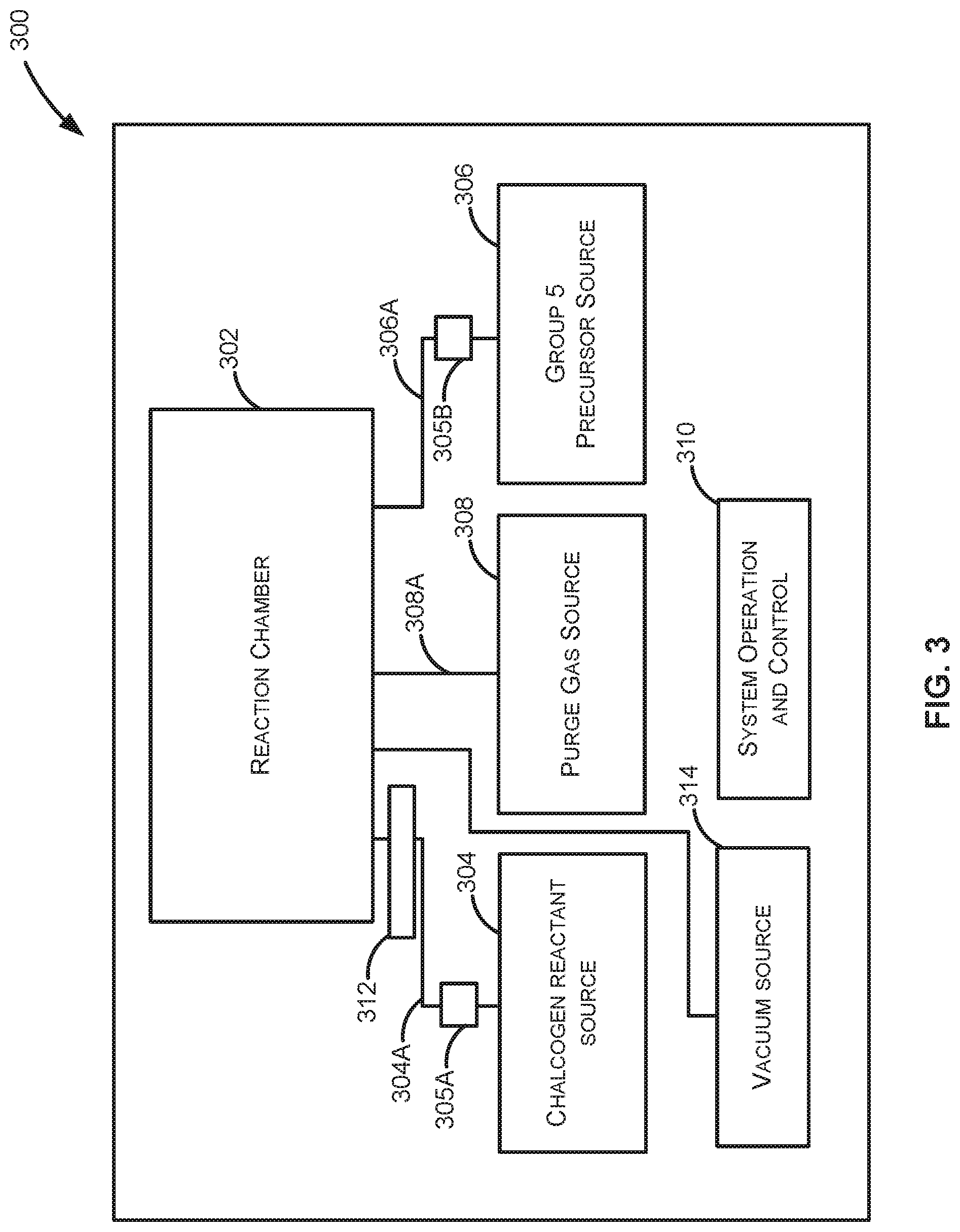
20. The method of claim 19, wherein a temperature within the reaction chamber during the step of annealing is less than 800.degree. C.
21. The method of claim 1, further comprising a step of etching the group 5 chalcogenide layer using an etchant comprising a metal halide.
22. A structure formed according to claim 1.
23. The structure of claim 22, wherein the layer comprises a 2D dichalcogenide material.
24. The structure of claim 23, wherein the dichalcogenide material is metallic.
25. The structure of claim 23, wherein the dichalcogenide material overlies and contacts semiconductor material.
26. The structure of claim 23, further comprising a capping layer overlying the dichalcogenide material
27. A device comprising the structure of claim 23.
28. The device of claim 27, wherein the device comprises one or more of a semiconductor device, a supercapacitor, a battery, and an electrochemical device.
29. A system for depositing a chalcogenide material according to the method of claim 1.
30. The system of claim 29 comprising a group 5 precursor source.
31. The system of claim 29, further comprising a chalcogen reactant source.
32. The system of claim 29, further comprising a system operation and control to control one or more of pressure and temperature within a reaction chamber.
Description
CROSS-REFERENCE TO RELATED APPLICATIONS
[0001] This application claims priority to U.S. Provisional Patent Application Ser. No. 62/895,453 filed Sep. 3, 2019 titled "METHODS AND APPARATUS FOR DEPOSITING A CHALCOGENIDE FILM AND STRUCTURES INCLUDING THE FILM," the disclosure of which is hereby incorporated by reference in its entirety.
PARTIES OF JOINT RESEARCH AGREEMENT
[0002] The invention claimed herein was made by, or on behalf of, and/or in connection with a joint research agreement between the University of Helsinki and ASM Microchemistry Oy. The agreement was in effect on and before the date the claimed invention was made, and the claimed invention was made as a result of activities undertaken within the scope of the agreement.
FIELD OF INVENTION
[0003] The present disclosure relates generally to methods and systems for depositing a chalcogenide film on a substrate. The disclosure also relates to structures including a chalcogenide film.
BACKGROUND OF THE DISCLOSURE
[0004] Group 5 and other transition metal dichalcogenides (TMDCs) can be represented by the formula MX.sub.2, where M represents a transition metal (e.g., group 5 metal) and X represents a chalcogenide, such as sulfur, selenium, or tellurium. Exemplary TMDCs include MoS.sub.2 and WSe.sub.2. TMDCs include semiconducting, semi-metallic, and metallic materials.
[0005] Most studies have examined properties of semiconducting TMDCs, in particular the properties of group 6 disulfides and selenides, such as MoS.sub.2, MoSe.sub.2, WS.sub.2, and WSe.sub.2. While the semiconducting TMDCs are indeed very important and perform well in some applications, such as field-effect transistors and photodetectors, for some applications, it is desired to have films with higher electrical conductivity. Some examples of such applications include various energy applications, such as water-splitting catalysis (hydrogen evolution reaction (HER) and oxygen evolution reaction (OER)), supercapacitors, and batteries. Furthermore, forming electrical contact to semiconducting TMDCs has turned out to be very difficult using traditional metals with a 3D crystal structure, such as gold and tungsten.
[0006] Group 5 dichalcogenides, namely VS.sub.2, VSe.sub.2, VTe.sub.2, NbS.sub.2, NbSe.sub.2, NbTe.sub.2, TaS.sub.2, TaSe.sub.2, and TaTe.sub.2 can be considered to be either metals or semimetals with high electrical conductivity. Many dichalcogenide of the group 5 dichalcogenides exhibit phase changes, becoming either superconducting at low temperatures and/or showing different charge density wave (CDW) phases at different temperatures, both of which properties may be useful for various electronic devices.
[0007] For many applications, it may be desirable to deposit the dichalcogenide material in two-dimensional (2D) (layered crystal structure) form. Currently, few, if any, methods are able to deposit uniform films of group 5 dichalcogenides in ultrathin (e.g., less than 10 nm or less than 5 nm) 2D form.
[0008] Mechanical exfoliation of bulk crystals has been used for fundamental studies, but such processes are very difficult to scale up for production. Physical vapor deposition (PVD) methods, including evaporation and molecular beam epitaxy (MBE) have been reported, mainly for the deposition of group 5 sulfides and selenides, respectively. Unfortunately, deposition of films using MBE uses very expensive UHV equipment. Chemical vapor deposition (CVD) is perhaps the most commonly applied technique to deposit group 5 dichalcogenides. However, CVD usually requires high temperatures of about 600.degree. C. to about 1000.degree. C. and depositing thin, continuous dichalcogenide films using CVD can be difficult.
[0009] Chalcogenization of metal or metal oxide films to form dichalcogenide material has also been reported. Chalcogenization may be more scalable and more capable of producing continuous films than the CVD processes reported so far, but the resulting chalcogen films can suffer from limited grain size and chalcogenization methods use relatively high reaction temperatures, which can be similar to temperatures used for CVD of dichalcogenide material. Some CVD processes operating at lower temperatures have been reported, but most of these reports deal with films that are at least hundreds of nanometers thick, which cannot be considered 2D.
[0010] Accordingly, improved methods for producing chalcogenide materials, such as 2D chalcogenide materials, are desired. Improved systems for forming the chalcogenide materials and structures including the chalcogenide materials are also desired.
[0011] Any discussion, including discussion of problems and solutions, set forth in this section has been included in this disclosure solely for the purpose of providing a context for the present disclosure, and should not be taken as an admission that any or all of the discussion was known at the time the invention was made or otherwise constitutes prior art.
SUMMARY OF THE DISCLOSURE
[0012] This summary is provided to introduce a selection of concepts in a simplified form. These concepts are described in further detail in the detailed description of example embodiments of the disclosure below. This summary is not intended to necessarily identify key features or essential features of the claimed subject matter, nor is it intended to be used to limit the scope of the claimed subject matter.
[0013] In accordance with exemplary embodiments of the present disclosure, methods for forming a structure including a layer comprising chalcogenide material, such as dichalcogenide material, are provided. While the ways in which the various drawbacks of the prior art are discussed in greater detail below, in general, exemplary methods include techniques suitable for forming (e.g., metallic or conducting) 2D films of dichalcogenide material. The (e.g., 2D or metallic) dichalcogenide material can be used to overcome the Fermi level pinning issues observed with 3D metals to significantly reduce contact resistance to another material, and for several other applications. Further exemplary embodiments relate to structures that include a layer comprising chalcogenide material, such as dichalcogenide material and/or to systems for performing methods and/or forming structures as described herein.
[0014] In accordance with exemplary embodiments of the disclosure, methods of forming a structure include providing a substrate within a reaction chamber, providing a group 5 precursor within the reaction chamber, and providing a chalcogen reactant within the reaction chamber. The method can include a cyclical deposition process, such as a cyclical chemical vapor deposition (CVD) and/or atomic layer deposition (ALD). Additionally or alternatively, the method can include forming a layer comprising a 2D group 5 chalcogenide on the substrate and/or forming a layer comprising a metallic group 5 chalcogenide on the substrate. The group 5 chalcogenide material can be or include group 5 dichalcogenide material. A temperature within the reaction chamber during one or more of the steps can be about 50.degree. C. to about 500.degree. C., about 100.degree. C. to about 600.degree. C., or about 300.degree. C. to about 500.degree. C. A pressure within the reaction chamber during one or more of the steps can be about 10.sup.-2 to about 1000 mbar, about 10.sup.-4 to about 100 mbar, about 10.sup.-2 to about 50 mbar, or about 10.sup.-1 to about 10 mbar. The group 5 precursor can be or include one or more of a tantalum precursor, a niobium precursor, and a vanadium precursor. The group 5 precursor can be or include a nitrogen-coordinated compound, such as a compound comprising one or more of an amide ligand and an amido ligand. Additionally or alternatively, the group 5 precursor can be or include a homoleptic compound or a heteroleptic compound. Exemplary chalcogen reactants can be or include one of more of a sulfur reactant, a selenium reactant, and a tellurium reactant. For example, the chalcogen reactant can include one or more of H.sub.2S, S(SiMe.sub.3).sub.2, Se(SiEt.sub.3).sub.2, alkyl substituents on the alkylsilyl group (SiR.sub.3), H.sub.2Se, and/or other precursors as described herein. Exemplary methods can further include a step of annealing--e.g., at a temperature less than 800.degree. C., or less than 600.degree. C., or less than 500.degree. C., or even less than 400.degree. C., or between about 400.degree. C. and about 500.degree. C. The step of annealing can be performed in chalcogen-containing (e.g., elemental S, Se, Te or H.sub.2S) environment. Additionally or alternatively, the environment can also include H.sub.2 or an inert atmosphere (e.g., N.sub.2, Ar, He) atmosphere--e.g., for a period of less than 1 hour, less than 30 minutes, less than 15 minutes, or less than 5 minutes.
[0015] In accordance with further embodiments of the disclosure, a structure is provided. The structure can include a substrate and a layer comprising a group 5 chalcogenide overlying the substrate. The layer can be a 2D group 5 chalcogenide, a metallic group 5 chalcogenide, and/or a dichalcogenide material. The substrate can include a layer of semiconductor material (e.g., semiconductor material including a chalcogenide material), and the layer comprising a group 5 chalcogenide can form a contact layer with the semiconductor material.
[0016] In accordance with further exemplary embodiments of the disclosure, a device includes a structure as described herein. Exemplary devices can include a semiconductor device, a supercapacitor, a battery, an electrochemical device, or the like.
[0017] In accordance with yet additional examples of the disclosure, a system for depositing a chalcogenide material is provided. The system can be used to perform a method and/or to form a structure, as described herein.
[0018] These and other embodiments will become readily apparent from the following detailed description of certain embodiments having reference to the attached figures; the invention not being limited to any particular embodiments disclosed.
BRIEF DESCRIPTION OF THE DRAWING FIGURES
[0019] While the specification concludes with claims particularly pointing out and distinctly claiming what are regarded as embodiments of the invention, the advantages of embodiments of the disclosure may be more readily ascertained from the description of certain examples of the embodiments of the disclosure when read in conjunction with the accompanying drawings, in which:
[0020] FIG. 1 illustrates a method in accordance with at least one embodiment of the disclosure;
[0021] FIG. 2 illustrates a structure in accordance with at least one embodiment of the disclosure; and
[0022] FIG. 3 illustrates an exemplary system in accordance with at least one embodiment of the disclosure.
[0023] It will be appreciated that elements in the figures are illustrated for simplicity and clarity and have not necessarily been drawn to scale. For example, the dimensions of some of the elements in the figures may be exaggerated relative to other elements to help improve understanding of illustrated embodiments of the present disclosure. Further, illustrations presented herein are not necessarily meant to be actual views of any particular material, structure, system, or device, but rather may be idealized representations that are used to facilitate descriptions of exemplary embodiments of the disclosure.
DETAILED DESCRIPTION OF EXEMPLARY EMBODIMENTS
[0024] Although certain embodiments and examples are disclosed below, it will be understood by those in the art that the invention extends beyond the specifically disclosed embodiments and/or uses of the invention and obvious modifications and equivalents thereof. Thus, it is intended that the scope of the invention disclosed should not be limited by the particular disclosed embodiments described below.
[0025] The present disclosure generally relates to methods of forming structures that include a layer comprising a group 5 chalcogenide, to structures formed using the methods, and to systems for performing the methods and/or forming the structures. Exemplary methods described herein can be used to form structures that include a dichalcogenide, a 2D group 5 chalcogenide and/or a metallic group 5 chalcogenide on the substrate. The structures can be used to form a variety of devices, such as a semiconductor device (e.g., as a contact layer to a semiconductor layer), a supercapacitor, a (e.g., lithium-ion) battery, an electrochemical (e.g., water-splitting catalysis) device, and the like.
[0026] As used herein, the term structure can include a substrate and a layer. A structure can form part of a device, such as a device as described herein. Structures can undergo further processing, such as deposition, etch, clean, and the like process steps to form a device.
[0027] As used herein, the term substrate can refer to any underlying material or materials upon which a layer can be deposited. A substrate can include a bulk material, such as silicon (e.g., single-crystal silicon) or other semiconductor material, and can include one or more layers, such as native oxides or other layers, overlying or underlying the bulk material. Further, the substrate can include various topologies, such as recesses, lines, and the like formed within or on at least a portion of a layer and/or bulk material of the substrate. By way of particular examples, a substrate may comprise one or more materials including, but not limited to, silicon (Si), germanium (Ge), germanium tin (GeSn), silicon germanium (SiGe), silicon germanium tin (SiGeSn), silicon carbide (SiC), or a group III-V semiconductor material, such as, for example, gallium arsenide (GaAs), gallium phosphide (GaP), or gallium nitride (GaN). In some embodiments, the substrate may comprise one or more dielectric materials including, but not limited to, oxides, nitrides, or oxynitrides. For example, the substrate may comprise a silicon oxide (e.g., SiO.sub.2), a metal oxide (e.g., Al.sub.2O.sub.3), a silicon nitride (e.g., Si.sub.3N.sub.4), or a silicon oxynitride. In some embodiments of the disclosure, the substrate may comprise an engineered substrate wherein a surface semiconductor layer is disposed over a bulk support with an intervening buried oxide (BOX) disposed therebetween. Patterned substrates can include features formed into or onto a surface of the substrate, for example, a patterned substrate may comprise partially fabricated semiconductor device structures, such as, for example, transistors and/or memory elements. In some embodiments, the substrate may contain monocrystalline surfaces and/or one or more secondary surfaces that may comprise a non-monocrystalline surface, such as a polycrystalline surface and/or an amorphous surface. Monocrystalline surfaces may comprise, for example, one or more of silicon, silicon germanium, germanium tin, germanium, or a III-V material. Polycrystalline or amorphous surfaces may include dielectric materials, such as oxides, oxynitrides, or nitrides, such as, for example, silicon oxides and silicon nitrides.
[0028] In this disclosure, the term gas can refer to material that is a gas at room temperature and pressure, a vaporized solid and/or a vaporized liquid, and may be constituted by a single gas or a mixture of gases, depending on the context. A gas other than the process gas, e.g., a gas introduced without passing through a gas distribution assembly, such as a showerhead, other gas distribution device, or the like, may be used for, e.g., sealing the reaction space, which includes a seal gas such as a rare gas. In some embodiments, the term "precursor" refers generally to a compound that participates in the chemical reaction that produces another compound, and particularly to a compound that constitutes a film matrix or a main skeleton of a film; the term "reactant" refers to a compound that activates a precursor, modifies a precursor, or catalyzes a reaction of a precursor, wherein the reactant may provide an element (such as a chalcogen) to a film matrix and may become a part of the film matrix. In some cases, the terms precursor and reactant can be used interchangeably. The term "inert gas" can refer to a gas that does not take part in a chemical reaction and/or a gas that excites a precursor when (e.g., RF) power is applied, but unlike a reactant, it may not become a part of a film to an appreciable extent.
[0029] As used herein, the term cyclic deposition can refer to a process in which sequential introduction of precursors (and/or reactants) into a reaction chamber is used to deposit a film over a substrate and includes deposition techniques such as atomic layer deposition (ALD), cyclical chemical vapor deposition, and hybrid atomic layer deposition and chemical vapor deposition processes.
[0030] As used herein, the term atomic layer deposition can refer to a vapor deposition process in which deposition cycles, for example, a plurality of consecutive deposition cycles, are conducted in a reaction chamber. Typically, during each cycle a precursor is chemisorbed to a deposition surface (e.g., a substrate surface or a previously deposited underlying surface, such as material from a previous ALD cycle), forming a monolayer or sub-monolayer that does not readily react with additional precursor (i.e., a self-limiting reaction). Thereafter, a reactant may subsequently be introduced into the process chamber for use in converting the chemisorbed precursor to the desired material on the deposition surface. Typically, this reactant is capable of further reaction with the precursor. Further, purging steps may be utilized during each cycle to remove excess precursor from the process chamber and/or remove excess reactant and/or reaction byproducts from the process chamber. The term ALD, as used herein, is also meant to include processes designated by related terms, such as chemical vapor atomic layer deposition, atomic layer epitaxy (ALE), molecular beam epitaxy (MBE), gas source MBE, or organometallic MBE, and chemical beam epitaxy when performed with alternating pulses of precursors and reactants, and optionally a purge (e.g., inert) gas.
[0031] As used herein, the term cyclical chemical vapor deposition or cyclic chemical vapor deposition can refer to any process wherein a substrate is sequentially exposed to two or more volatile precursors, which react and/or decompose on a substrate to produce a desired deposition.
[0032] As used herein, the term film can refer to any continuous or non-continuous structures and material, such as material deposited by the methods disclosed herein. For example, a film can include 2D materials or partial or full molecular layers or partial or full atomic layers or clusters of atoms and/or molecules. A film can include material with pinholes, but still be at least partially continuous. The terms film and layer can be used interchangeably.
[0033] As used herein, the terms 2D material, two-dimensional material, or simply 2D can refer to a nanometer scale crystalline material of about one, two or three atoms in thickness. Such terms can also refer to an ordered nanometer scale crystalline structure composed of multiple monolayers of crystalline materials of approximately three atoms in thickness per monolayer.
[0034] As used herein, the term chalcogen reactant can refer to a reactant containing a chalcogen, wherein a chalcogen is an element from group 16 of the periodic table. In accordance with various examples of the disclosure, the chalcogen is selected from the group consisting of sulfur, selenium, and tellurium.
[0035] As used herein, the term group 5 chalcogenide can refer to a material, which can be represented by a chemical formula that includes one or more elements from group 5 of the periodic table and one or more chalcogen elements. By way of particular examples, the chemical formulas of group 5 chalcogenides can include one or more of vanadium, niobium, and tantalum.
[0036] As used herein, the term group 5 precursor can refer to a precursor comprising a group 5 metal, such as at least one of tantalum, niobium, and vanadium.
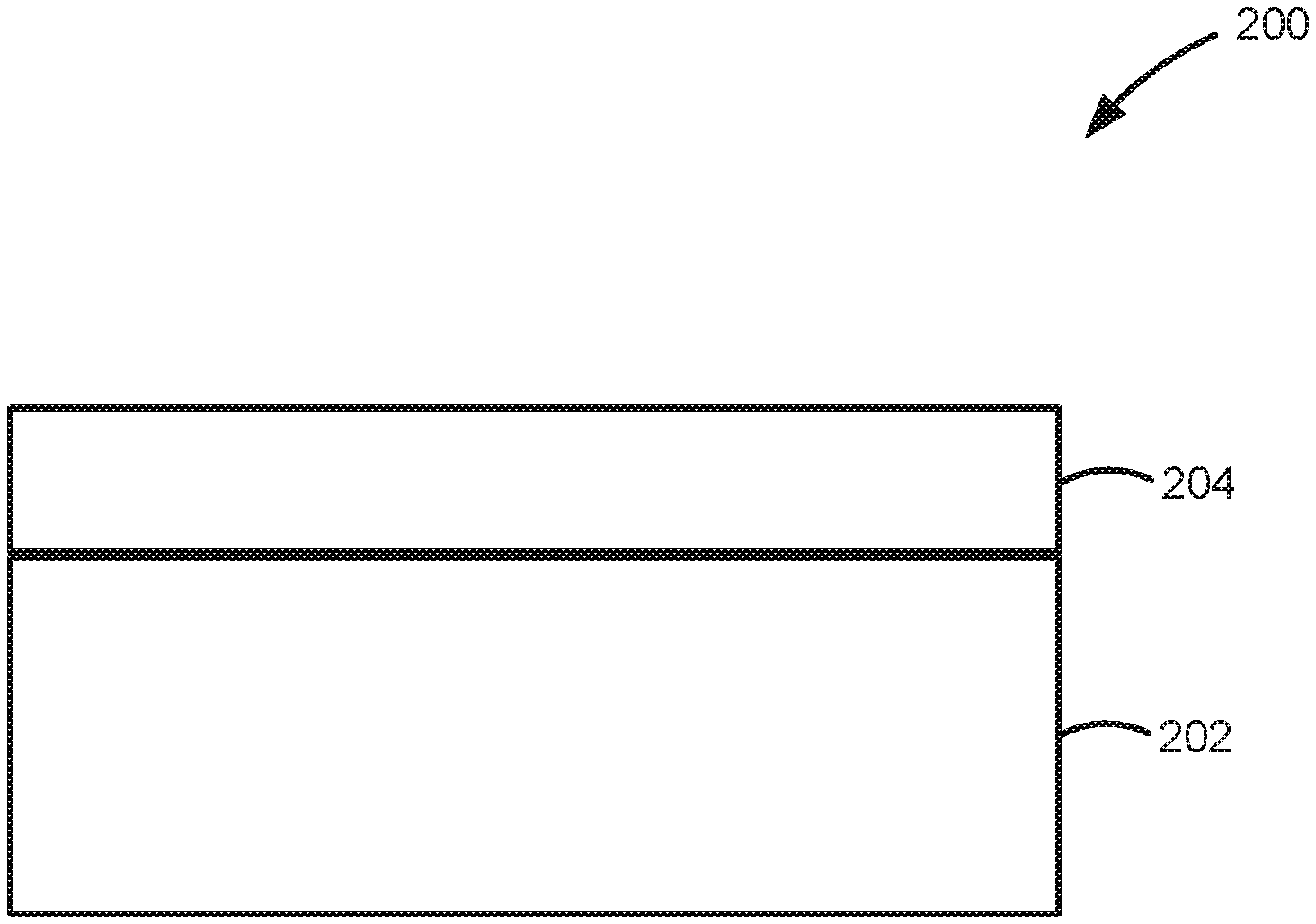
[0037] As used herein, the term halide precursor can refer to a halide precursor comprising a halide component, such as at least one of fluorine, chlorine, iodine, and bromine.
[0038] As used herein, the term metalorganic precursor can refer to a group 5 metal metalorganic precursor. The terms metalorganic and organometallic can be used interchangeably and can refer to organic compounds containing a metal species. Organometallic compounds can be considered to be a subclass of metalorganic compounds having direct metal-carbon bonds.
[0039] As used herein, the term tantalum precursor can refer to a precursor that can be represented by a chemical formula that includes tantalum. Similarly, the term niobium precursor can refer to a precursor that can be represented by a chemical formula that includes niobium and the term vanadium precursor can refer to a precursor that can be represented by a chemical formula that includes vanadium.
[0040] A number of example materials are given throughout the disclosure; it should be noted that the chemical formulas given for each of the example materials should not be construed as limiting and that the non-limiting example materials given should not be limited by a given example stoichiometry.
[0041] As noted above, typical methods of forming a layer of chalcogenide material include mechanical exfoliation of a bulk chalcogenide crystal, physical vapor deposition, chemical vapor deposition, and chalcogenization. While such methods can be used to deposit or form some chalcogenide films for some applications, such methods are generally not suitable for forming layers comprising group 5 chalcogenides to a desired thickness and/or accuracy. In addition, such techniques may require undesirably high temperatures to deposit or form chalcogenide material and/or cannot be used to form 2D and/or metallic group 5 chalcogenides.
[0042] In contrast, exemplary methods of the present disclosure can be used to form a structure that includes a layer comprising a group 5 chalcogenide, such as group 5 dichalcogenides, 2D, and/or metallic layers comprising a group 5 chalcogenide.
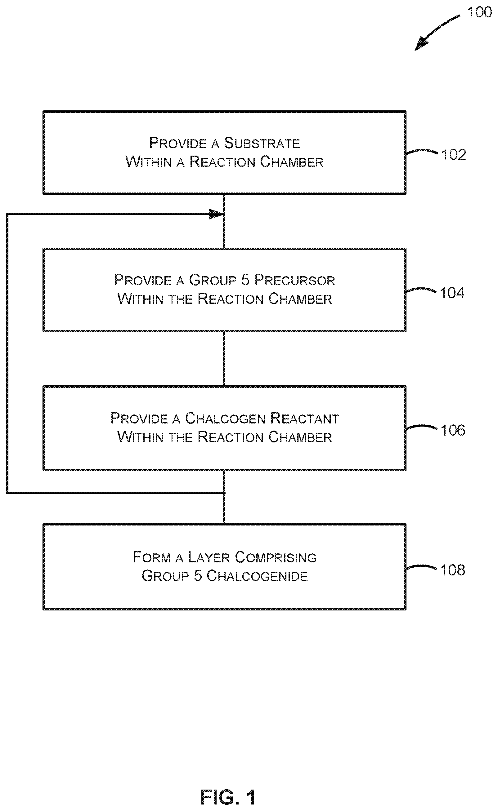
[0043] Turning now to the figures, FIG. 1 illustrates a method 100 in accordance with exemplary embodiments of the disclosure. Method 100 includes the steps of providing a substrate within a reaction chamber (step 102), providing a group 5 precursor within the reaction chamber (step 104), providing a chalcogen reactant within the reaction chamber (step 106), and forming a layer comprising a group 5 chalcogenide on the substrate (step 108). As set forth in more detail below, although illustrated as separate steps, at least a portion of the layer comprising a group 5 chalcogenide can begin to form as the chalcogen reactant is introduced within the reaction chamber.
[0044] In accordance with exemplary embodiments of the disclosure, method 100 comprises a cyclical deposition method, such as a cyclical chemical vapor deposition method, an ALD method, or a hybrid ALD/CVD method. Such methods are generally scalable and can offer film thickness control at an atomic level, which is desirable in the formation of high quality 2D and/or metallic group 5 chalcogenide (e.g., dichalcogenide) materials. In addition, cyclic deposition methods with surface control in reactions, such as ALD, are generally conformal, thereby providing an ability to uniformly coat three-dimensional structures with desired material.
[0045] Group 5 chalcogenide films may be susceptible to oxidation either during the deposition process or when exposed to ambient conditions. Therefore, cyclical deposition methods, which do not incorporate oxide phases into the chalcogenide film during deposition, and/or that mitigate the oxidation of the group 5 chalcogenide films when exposed to ambient conditions, may be desirable.
[0046] In cyclical processes, one deposition cycle may comprise exposing the substrate to a first vapor phase reactant, removing any unreacted first reactant and reaction byproducts from the reaction space, and exposing the substrate to a second vapor phase reactant, followed by a second removal step. The first reactant may comprise a group 5 precursor, and the second reactant may comprise a chalcogen containing precursor (a chalcogen reactant).
[0047] In some embodiments, the cyclical deposition may be a hybrid ALD/CVD or cyclical CVD process. For example, in some embodiments, the deposition rate of the ALD process may be low compared with a CVD process. One approach to increase the deposition rate may be that of operating at a higher substrate temperature than that typically employed in an ALD process, resulting in a chemical vapor deposition process, but still taking advantage of the sequential introduction of precursors; such a process may be referred to as cyclical CVD. In some embodiments, a cyclical CVD process may comprise the introduction of two or more precursors into the reaction chamber wherein there may be a time period of overlap between the two or more precursors in the reaction chamber resulting in both an ALD component of the deposition and a CVD component of the deposition. For example, a cyclical CVD process may comprise the continuous flow of a first precursor and the periodic pulsing of a second precursor into the reaction chamber.
[0048] A reaction chamber for the exemplary cyclical deposition process 100 may be part of a system, such as system 300, described below. Exemplary reactors including a reaction chamber that are suitable for use with method 100 include ALD reactors, as well as CVD reactors equipped with appropriate equipment and means for providing the precursors/reactants. According to some embodiments, the reactor includes a showerhead to distribute one or more gases within the reaction chamber. In some embodiments, the reactor is a spatial ALD reactor, in which the reactants/precursors are spatially separated by moving the substrate during processing.
[0049] In some embodiments, a batch reactor may be used. In some embodiments, a vertical batch reactor is utilized in which a boat that contains substrates can rotate during processing. In some embodiments, the substrate(s) can rotate during processing. In other embodiments, the batch reactor comprises a mini-batch reactor configured to accommodate 10 or fewer wafers, 8 or fewer wafers, 6 or fewer wafers, 4 or fewer wafers, or 2 wafers. In some embodiments in which a batch reactor is used, wafer-to-wafer non-uniformity is less than 3% (lsigma), less than 2%, less than 1% or even less than 0.5%.
[0050] The deposition processes described herein can optionally be carried out in a reactor or reaction chamber connected to a cluster tool. In a cluster tool, because each reaction chamber can be dedicated to one type of process, the temperature of the reaction chamber in each module can be kept constant, which improves the throughput compared to a reactor in which the substrate is heated up to the process temperature before each run. Additionally, in a cluster tool, it is possible to reduce the time to pump the reaction space to the desired process pressure levels between substrates.
[0051] A stand-alone reactor can be equipped with a load-lock. In that case, it may not be necessary to cool down the reaction chamber between each run.
[0052] In some embodiments of the disclosure, the reaction chamber may be subjected to a pre-annealing process prior to loading the substrate within the reaction chamber or with the substrate pre-loaded into the reaction chamber. For example, the pre-annealing process may be utilized to reduce the concentration of at least one of water and/or oxygen, within the reaction chamber. Therefore, some embodiments of the disclosure may further comprise pre-annealing the reaction chamber prior to film deposition at a temperature of greater than 400.degree. C., or greater than 500.degree. C., or greater than 600.degree. C., or even greater than 700.degree. C. In some embodiments, the pre-annealing of the reaction chamber at high temperature may be performed for a time period of less than 60 minutes, or less than 30 minutes, or less than 15 minutes, or less than 10 minutes, or even less than 5 minutes.
[0053] Referring again to FIG. 1, step 102 includes providing a substrate within a reaction chamber. During step 102, the substrate can be heated to a deposition temperature, and the reaction chamber can be brought to a desired operating pressure.
[0054] As a non-limiting example, the substrate may be heated to a deposition temperature. For example, in some embodiments, methods may comprise heating the substrate (and/or reaction chamber) to a temperature of between approximately 50.degree. C. and approximately 500.degree. C., between about 100.degree. C. and about 600, .degree. C., between about 300.degree. C. and about 500.degree. C., or even heating the substrate to a temperature of between approximately 350.degree. C. and approximately 450.degree. C. Of course, the appropriate temperature window for any given cyclical deposition process, such as for an ALD reaction, will depend upon the surface termination and reactant species involved. Here, the temperature varies depending on the precursors being used and is generally at or below about 700.degree. C. In some embodiments, the deposition temperature is generally at or above about 100.degree. C. for vapor deposition processes. In some embodiments, the deposition temperature is between about 100.degree. C. and about 600.degree. C., and in some embodiments, the deposition temperature is between about 300.degree. C. and about 500.degree. C. In some embodiments, the deposition temperature is below about 500.degree. C., or below about 475.degree. C., or below about 450.degree. C., or below about 425.degree. C., or below about 400.degree. C., or below about 375.degree. C., or below about 350.degree. C., or below about 325.degree. C. or below about 300.degree. C. In some instances, the deposition temperature can be below about 250.degree. C., or below about 200.degree. C., or below about 150.degree. C., or below about 100.degree. C., for example, if additional reactants or reducing agents are used in the process. In some instances, the deposition temperature can be above about 20.degree. C., above about 50.degree. C. and above about 75.degree. C. The pressure within the reaction chamber can be between about 10.sup.-7 to about 1000 mbar, about 10.sup.-4 to about 100 mbar, about 10.sup.-2 to about 50 mbar, or about 10.sup.-1 to about 10 mbar.
[0055] During step 104, a group 5 precursor is provided within the reaction chamber. In accordance with various embodiments of the disclosure, the group 5 precursor includes one or more of a tantalum precursor, a niobium precursor, and a vanadium precursor. In some embodiments, the group 5 precursor comprises at least one of a metalorganic compound, an organometallic compound, and a metal halide compound. In accordance with exemplary embodiments, the group 5 precursor comprises a nitrogen-coordinated compound. In some embodiments of the disclosure, the group 5 precursor comprises one or more bidentate ligands which are bonded to a group 5 element through nitrogen and/or oxygen atoms. In some embodiments, the group 5 precursor comprises one or more ligands which are bonded to a group 5 atom through nitrogen, oxygen, and/or carbon.
[0056] In some embodiments, the metalorganic precursor may be nitrogen coordinated--e.g., comprise one or more of an amide ligand and an amido ligand, or an imido ligand. In some embodiments, the group 5 precursor comprises a heteroleptic compound. In other embodiments, the group 5 precursor comprises a homoleptic compound.
[0057] By way of examples, a tantalum precursor can be or include one or more of a tantalum metalorganic compound, a tantalum organometallic compound, and a tantalum halide compound. In accordance with exemplary embodiments, the tantalum precursor comprises a nitrogen-coordinated compound, such as one or more of amides, imides, and amidinates. In some embodiments, the tantalum metalorganic precursor comprises one or more of amide ligand (e.g., Ta(NEtMe).sub.5 and Ta(NMe.sub.2).sub.5) and an imido ligand (e.g., both types of ligands, such as Ta(NtBu)(NEt.sub.2).sub.3). In some embodiments, the tantalum precursor comprises a heteroleptic compound. A heteroleptic compound can comprise Cp and halogen such as chloride, or Cp and alkylamine, or amide and halide, such as chloride. In other embodiments, the tantalum precursor comprises a homoleptic compound. In some embodiments, the tantalum halide precursor may comprise at least one halide ligand while the rest of the ligands are different, such as metalorganic or organometallic ligands as described herein. In some embodiments, the tantalum halide precursor may comprise one, two, three, four, or five halide ligands. In some embodiments, the tantalum metalorganic precursor may comprise at least one of a tantalum alkylamide precursor, a tantalum cyclopentadienyl-ligand containing precursor, or other metalorganic tantalum precursors. In some embodiments of the disclosure, the tantalum precursor comprises one or more bidentate ligands which are bonded to tantalum through nitrogen and/or oxygen atoms. In some embodiments, the tantalum precursor comprises one or more ligands which are bonded to tantalum through nitrogen, oxygen, and/or carbon. In some embodiments, the tantalum precursor is not halide. In some embodiments, the tantalum precursor does not comprise a halogen. In some embodiments, a ligand can include one or more of an alkoxo, an amidinate, and/or a pyrazolate group.
[0058] In some embodiments, the tantalum halide may comprise at least one of a tantalum chloride, a tantalum iodide, a tantalum bromide, and a tantalum fluoride. In some embodiments, the tantalum chloride may comprise tantalum pentachloride (TaCl.sub.5). In some embodiments, the tantalum iodide may comprise tantalum pentaiodide (TaI.sub.5). In some embodiments, the tantalum bromide may comprise tantalum pentabromide (TaBr.sub.5). In some embodiments, the tantalum fluoride may comprise tantalum pentafluoride (TaF.sub.5). Suitable tantalum halide precursors can be selected from any combination or subset of the above exemplary tantalum halide precursors.
[0059] By way of particular examples, the tantalum precursor can be or include one or more of pentakis(dimethylamido)tantalum (Ta(NMe.sub.2).sub.5), pentakis(diethylamido)tantalum (Ta(NEt.sub.2).sub.5), tris(diethylamido)(tert-butylimido)tantalum (Ta(N.sup.tBu)(NEt.sub.2).sub.3), tris(dimethylamido) (tert-butylimido)tantalum (Ta(N.sup.tBu)(NMe.sub.2).sub.3), tris(ethylmethylamido)(tert-butylimido)tantalum (Ta(N.sup.tBu)(NEtMe).sub.3), tris(diethylamido)(ethylimido)tantalum (Ta(NEt)(NEt.sub.2).sub.3), tris(dimethylamido)(tert-amylimido)tantalum (Ta(NtAmyl)(NMe.sub.2).sub.3), bis(diethylamido)cyclopentadienyl(tert-butylimido)tantalum (TaCp(N.sup.tBu)(NEt.sub.2).sub.2) (dimethylamido)bis(N,N'-isopropylacetamidinato)(tert-butylimido)tantalum (Ta(N.sup.tBu)(.sup.iPrAMD).sub.2(NMe.sub.2)), (tert-butylimido)tris(3,5-di-tert-butylpyrazolate)tantalum, (Ta(N.sup.tBu)(.sup.tBu.sub.2pz).sub.3), (isopropylimido)tris(tert-butoxy)tantalum (Ta(N.sup.iPr)(O.sup.tBu).sub.3), and (tert-butylimido)tris(tert-butoxy)tantalum (Ta(N.sup.tBu)(O.sup.tBu).sub.3), tantalum pentachloride (TaCl.sub.5), tantalum pentaiodide (TaI.sub.5), tantalum pentabromide (TaBr.sub.5), and tantalum pentaethoxide (Ta(OEt).sub.5). Other suitable compounds include changing the alkyl substituent(s) in amido or imido ligands of any of the above compounds. Suitable tantalum precursors can be selected from any combination or subset (e.g., one or more, two or more, and the like) of the above exemplary tantalum precursors.
[0060] The niobium precursor can be or include one or more of a niobium metalorganic compound, a niobium organometallic compound, and a niobium halide compound. In accordance with exemplary embodiments, the niobium precursor comprises a nitrogen-coordinated compound, such as one or more of amides, imides, and amidinates. In some embodiments, the tantalum metalorganic precursor comprises one or more of an amide ligand (e.g., Nb(NEtMe).sub.5 and Nb(NMe.sub.2).sub.5) and an imido ligand (e.g., both types of ligands, such as Nb(N.sup.tBu)(NEt.sub.2).sub.3). In some embodiments, the niobium precursor comprises a heteroleptic compound. A heteroleptic compound can comprise Cp and halogen such as chloride, or Cp and alkylamine, or amide and halide, such as chloride. In other embodiments, the niobium precursor comprises a homoleptic compound. In some embodiments, the niobium halide precursor may comprise at least one halide ligand while the rest of the ligands are different, such as metalorganic or organometallic ligands as described herein. In some embodiments, the niobium halide precursor may comprise one, two, three, four, or five halide ligands. In some embodiments, the niobium metalorganic precursor may comprise at least one of a niobium alkylamide precursor, a niobium cyclopentadienyl-ligand containing precursor, or other metalorganic niobium precursors. In some embodiments of the disclosure, the niobium precursor comprises one or more bidentate ligands which are bonded to niobium through nitrogen and/or oxygen atoms. In some embodiments, the niobium precursor comprises one or more ligands which are bonded to niobium through nitrogen, oxygen, and/or carbon. In some embodiments, the niobium precursor is not halide. In some embodiments, the niobium precursor does not comprise a halogen. In some embodiments, a ligand can include one or more of an alkoxo, an amidinate, and/or a pyrazolate group.
[0061] In some embodiments, the niobium halide precursor may comprise at least one of a niobium chloride, a niobium iodide, a niobium bromide, and a niobium fluoride. In some embodiments, the niobium chloride may comprise niobium pentachloride (NbCl.sub.5). In some embodiments, the niobium iodide may comprise niobium pentaiodide (NbI.sub.5). In some embodiments, the niobium bromide may comprise niobium pentabromide (NbBr.sub.5). In some embodiments, the niobium fluoride may comprise niobium pentafluoride (NbF.sub.5). Suitable niobium halide precursors can be selected from any combination or subset of the above exemplary niobium halide precursors.
[0062] By way of particular examples, the niobium precursor can be or include one or more of tetra kis(2,2,6,6,-tetra methylheptane-3,5-dionato)niobium (Nb(thd).sub.4), pentakis(dimethylamido)niobium (Nb(NMe.sub.2).sub.5), pentakis(diethylamido)niobium (Nb(NEt.sub.2).sub.5), tris(diethylamido)(tert-butylimido)niobium (Nb(N.sup.tBu)(NEt.sub.2).sub.3), tris(dimethylamido)(tert-butylimido)niobium (N b(N.sup.tBu)(NMe.sub.2).sub.3), tris(ethylmethylamido)(tert-butylimido)niobium (Nb(N.sup.tBu)(NEtMe).sub.3), (tert-amylimido)tris(tert-butoxy)niobium (Nb(N.sup.tAmyl)(O.sup.tBu).sub.3) niobium pentafluoride (NbF.sub.5), niobium pentachloride (NbCl.sub.5), niobium pentaiodide (NbI.sub.5), niobium pentabromide (NbBr.sub.5), or niobium pentaethoxide (Nb(OEt).sub.5). Other suitable compounds include changing the alkyl substituent(s) in amido or imido ligands of any of the above compounds. Suitable niobium precursors can be selected from any combination or subset of the above exemplary niobium precursors.
[0063] The vanadium precursor can be or include one or more of a vanadium metalorganic compound, a vanadium organometallic compound, and a vanadium halide compound. In accordance with exemplary embodiments, the niobium precursor comprises a nitrogen-coordinated compound, such as one or more of amides, imides, and amidinates. In some embodiments, the vanadium metalorganic precursor comprises one or more of an amide ligand and an amido ligand (e.g., both types of ligands). In some embodiments, the vanadium precursor comprises a heteroleptic compound. A heteroleptic compound can comprise Cp and halogen such as chloride, or Cp and alkylamine, or amide and halide, such as chloride. In other embodiments, the vanadium precursor comprises a homoleptic compound. In some embodiments, the vanadium halide precursor may comprise at least one halide ligand while the rest of the ligands are different, such as metalorganic or organometallic ligands as described herein. In some embodiments, the vanadium halide precursor may comprise one, two, three, four, or five halide ligands. In some embodiments, the vanadium metalorganic precursor may comprise at least one of a vanadium alkylamide precursor, a vanadium cyclopentadienyl-ligand containing precursor, or other metalorganic vanadium precursors. In some embodiments of the disclosure, the vanadium precursor comprises one or more bidentate ligands which are bonded to vanadium through nitrogen and/or oxygen atoms. In some embodiments, the vanadium precursor comprises one or more ligands which are bonded to vanadium through nitrogen, oxygen, and/or carbon. In some embodiments, the vanadium precursor is not halide. In some embodiments, the vanadium precursor does not comprise a halogen. In some embodiments, a ligand can include one or more of an alkoxo, an amidinate, and/or a pyrazolate group.
[0064] In some embodiments, the vanadium halide precursor may comprise at least one of a vanadium chloride, a niobium iodide, and a vanadium bromide. In some embodiments, the vanadium chloride may comprise vanadium tetrachloride (VCl.sub.4). In some embodiments, the vanadium iodide may comprise vanadium triiodide (Vl.sub.3). In some embodiments, the vanadium bromide may comprise vanadium tribromide (VBr.sub.3). In some embodiments, the vanadium fluoride may comprise vanadium pentafluoride (VF.sub.5). Suitable vanadium halide precursors can be selected from any subset of the above exemplary vanadium halide precursors.
[0065] By way of particular examples, the vanadium precursor can be or include one or more of tetrakis(ethylmethylamido)vanadium (V(NEtMe).sub.4), tetrakis(dimethylamido)vanadium (V(NMe.sub.2).sub.4), tetra kis(diethylamido)vanadium (V(NEt.sub.2).sub.4), tris(N,N'-diisopropylacetamidinato)vanadium (V('PrAMD).sub.3), tris(acetylacetonato)vanadium (V(acac).sub.3), vanadium pentafluoride (VF.sub.5), and vanadium tetrachloride (VCl.sub.4). Other suitable compounds include changing the alkyl substituent(s) in amido or imido ligands of any of the above compounds. Suitable vanadium precursors can be selected from any subset of the above exemplary vanadium precursors.
[0066] In some embodiments, step 104 includes pulsing the group 5 precursor within the reaction chamber for a time period between about 0.01 seconds and about 60 seconds, between about 0.05 seconds and about 10 seconds, or between about 0.1 seconds and about 5.0 seconds. In addition, during the pulsing of the group 5 precursor within the reaction chamber, the flow rate of the group 5 precursor may be less than 2000 sccm, or less than 500 sccm, or even less than 100 sccm, or be from about 1 to about 2000 sccm, from about 5 to about 1000 sccm, or from about 10 to about 500 sccm.
[0067] In accordance with some examples of the disclosure, etching of material can occur during step 104, particularly when the group 5 precursor includes a metal halide. An amount of etching can be manipulated by controlling one or more of a temperature, pressure, flowrate, precursor dose, and the selection/composition of the group 5 precursor.
[0068] In some embodiments, the purity of the group 5 precursor may influence the composition of the deposited film and therefore high purity sources of the group 5 precursor may be utilized. For example, in some embodiments, the group 5 precursor may comprise a group 5 precursor with a purity of greater than or equal to 99.99%.
[0069] In some embodiments, the group 5 precursor may be contained in a vessel and one or more heaters may be associated with the vessel to control the temperature of the group 5 precursor and subsequently the partial pressure of the group 5 precursor. In some embodiments of the disclosure, the group 5 precursor within the vessel may be heated to a temperature between approximately 20.degree. C. and approximately 300.degree. C. For example, in some embodiments, the group 5 precursor may be heated to a temperature from about 30.degree. C. to about 250.degree. C., or from about 40.degree. C. to about 225.degree. C., or from about 50.degree. C. to about 150.degree. C., depending on the precursor.
[0070] In some embodiments, a vessel containing the group 5 precursor may be connected to a source of one or more carrier gases. The carrier gas may be introduced into the vessel and drawn over the surface of, or bubbled through, the metal precursor contained within the vessel. The resulting evaporation of the group 5 precursor causes a vapor of the group 5 precursor to become entrained in the carrier gas to thereby dispense the group 5 precursor to a reaction chamber.
[0071] In some embodiments, in addition to utilizing high purity group 5 precursors, the carrier gas may be further purified to remove unwanted impurities. Therefore, some embodiments of the disclosure may further comprise flowing a carrier gas through a vessel containing a source of the group 5 precursor to transport the group 5 precursor to the reaction chamber. Further embodiments of the disclosure may comprise flowing the carrier through a gas purifier prior to entering the source of the group 5 precursor to reduce the concentration of at least one of water and oxygen within the carrier gas.
[0072] In some embodiments, the water concentration within the carrier gas may be reduced to less than 10 parts per million, or less than 1 part per million, or less than 100 parts per billion, or less than 10 parts per billion, or less than 1 part per billion, or even less than 100 parts per trillion.
[0073] In some embodiments, the oxygen concentration within the carrier gas may be reduced to 10 parts per million, or less than 1 part per million, or less than 100 parts per billion, or less than 10 parts per billion, or less than 1 part per billion, or even less than 100 parts per trillion.
[0074] In some embodiments, the hydrogen (H.sub.2) concentration within the carrier gas may be reduced to less than 100 parts per trillion. In some embodiments, the carbon dioxide (CO.sub.2) concentration within the carrier gas may be reduced to less than 100 parts per trillion. In some embodiments, the carbon monoxide (CO) concentration within the carrier gas may be reduced to less than 100 parts per trillion.
[0075] In some embodiments, the carrier gas may comprise nitrogen gas (N.sub.2) and the carrier gas purifier may comprise a nitrogen gas purifier.
[0076] In some embodiments of the disclosure, the group 5 precursor may be fed through a gas purifier prior to entering the reaction chamber in order to reduce the concentration of at least one of water or oxygen, within the group 5 precursor.
[0077] In some embodiments, the water concentration within the group 5 precursor may be reduced to less than 1 atomic-%, or less than 1000 parts per million, or less than 100 parts per million, or less than 10 parts per million, or less than 1 part per million, or less than 100 parts per billion, or even less than 100 parts per trillion.
[0078] In some embodiments, the oxygen concentration within the group 5 precursor may be reduced to less than 1 atomic-%, or less than 1000 parts per million, or less than 100 parts per million, or less than 10 parts per million, or less than 1 part per million, or less than 100 parts per billion, or even less than 100 parts per trillion.
[0079] Not to be bound by any theory or mechanism, but it is believed the reduction of at least one of the water concentrations and the oxygen concentration within the carrier gas and/or the group 5 precursor may allow for the deposition of a group 5 chalcogenide film with the desired composition whilst preventing the deposition of oxide phases at desired deposition temperatures.
[0080] As part of step 104, the reaction chamber can be purged using a vacuum and/or an inert gas, such as one or more of argon (Ar) and nitrogen (N.sub.2), to mitigate gas phase reactions between reactants and enable self-saturating surface reactions--e.g., in the case of ALD. Additionally or alternatively, the substrate may be moved to separately contact a first vapor phase reactant and a second vapor phase reactant. Surplus chemicals and reaction byproducts, if any, can be removed from the substrate surface, such as by purging the reaction space or by moving the substrate, before the substrate is contacted with the next reactive chemical (step 106).
[0081] For example, in some embodiments of the disclosure, the methods may include a purge cycle wherein the substrate surface is purged for a time period of less than approximately 5.0 seconds, or less than approximately 2.0 seconds, or even less than approximately 1.0 seconds. In some embodiments, the substrate surface is purged for a time period between about 0.01 seconds and about 60 seconds, or between about 0.05 seconds and about 10 seconds, or between about 0.1 seconds and about 5 seconds. Excess group 5 precursor and any reaction byproducts may be removed with the aid of a vacuum generated by a pumping system.
[0082] Step 106 includes providing a chalcogen reactant within the reaction chamber. Any number of chalcogen reactants can be used in the cyclical deposition processes disclosed herein. In some embodiments, a chalcogen reactant is selected from the following list: H.sub.2S, H.sub.2Se, H.sub.2Te, (CH.sub.3).sub.2S, (NH.sub.4).sub.2S, dimethylsulfoxide ((CH.sub.3).sub.2SO), (CH.sub.3).sub.2Se, (CH.sub.3).sub.2Te, elemental or atomic S, Se, Te, other precursors containing chalcogen-hydrogen bonds, such as H.sub.2S.sub.2, H.sub.2Se.sub.2, H.sub.2Te.sub.2, or chalcogenols with the formula R--Y--H, wherein R can be a substituted or unsubstituted hydrocarbon, preferably a C.sub.1-C.sub.8 alkyl or substituted alkyl, such as an alkylsilyl group, more preferably a linear or branched C.sub.1-C.sub.5 alkyl group, and Y can be S, Se, or Te. In some embodiments, a chalcogen reactant is a thiol with the formula R--S--H, wherein R can be substituted or unsubstituted hydrocarbon, preferably a C.sub.1-C.sub.8 alkyl group, more preferably a linear or branched C.sub.1-C.sub.5 alkyl group. In some embodiments, a chalcogen reactant has the formula (R.sub.3Si).sub.2Y, wherein R.sub.3Si is an alkylsilyl group and Y can be S, Se or Te. In some embodiments, a chalcogen reactant comprises S or Se. In some embodiments, a chalcogen precursor comprises S. In some embodiments, a chalcogen precursor does not comprise S. In some embodiments, the chalcogen precursor may comprise an elemental chalcogen, such as elemental sulfur. In some embodiments, a chalcogen precursor does comprise Te. In some embodiments, a chalcogen precursor does not comprise Te. In some embodiments, a chalcogen precursor does comprise Se. In some embodiments, a chalcogen precursor does not comprise Se. In some embodiments, a chalcogen precursor is selected from precursors comprising S, Se and Te. In some embodiments, a chalcogen precursor comprises H.sub.2S.sub.n, wherein n is from 4 to 10. By way of examples, the chalcogen reactant can include one or more of reactant, which may comprise hydrogen sulfide (H.sub.2S), hydrogen selenide (H.sub.2Se), dimethyl sulfide ((CH.sub.3).sub.2S), Cert-butylthiol ((CH.sub.3).sub.3CSH), and/or 2-methylpropane-2-thiol, and dimethyl telluride ((CH.sub.3).sub.2Te).
[0083] In some embodiments, suitable chalcogen reactants may include any number of chalcogen-containing compounds. In some embodiments, a chalcogen reactant may comprise at least one chalcogen-hydrogen bond. In some embodiments, the chalcogen precursor may comprise a chalcogen plasma, chalcogen atoms or chalcogen radicals. In some embodiments where an energized chalcogen reactant is desired, a plasma may be generated in the reaction chamber or upstream of the reaction chamber. In some embodiments, the chalcogen reactant does not comprise an energized chalcogen precursor, such as plasma, atoms or radicals. In some embodiments, the chalcogen reactant may comprise a chalcogen plasma, chalcogen atoms or chalcogen radicals formed from a chalcogen reactant comprising a chalcogen-hydrogen bond, such as H.sub.2S. In some embodiments, a chalcogen reactant may comprise a chalcogen plasma, chalcogen atoms or chalcogen radicals such as a plasma comprising sulfur, selenium or tellurium, preferably a plasma comprising sulfur. In some embodiments, the plasma, atoms, or radicals comprise tellurium. In some embodiments, the plasma, atoms or radicals comprise selenium. In some embodiments, the chalcogen precursor does not comprise a tellurium precursor.
[0084] In some embodiments, the purity of the chalcogen reactants may influence the composition of the deposited film and therefore high purity sources of the chalcogen containing vapor phase reactant may be utilized. In some embodiments, the chalcogen reactant may have a purity of greater than or equal to 99.5%. As a non-limiting example, the chalcogen reactant may comprise hydrogen sulfide (H.sub.2S) with a purity of greater than or equal to 99.5%.
[0085] In some embodiments, in addition to utilizing high purity chalcogen reactants, the chalcogen precursor gas may be further purified to remove unwanted impurities. Therefore, some embodiments of the disclosure may further comprise flowing a chalcogen reactant through a gas purifier prior to entering the reaction chamber to reduce the concentration of at least one of water or oxygen within the chalcogen containing vapor phase reactant.
[0086] In some embodiments, the water or oxygen concentration within the chalcogen reactant may be reduced to less than 5 atomic-%, or less than 1 atomic-%, or less than 1000 parts per million, or less than 100 parts per million, or less than 10 parts per million, or less than 1 part per million, or less than 100 parts per billion, or less than 10 parts per billion, or even less than 1 part per billion.
[0087] Not to be bound by any theory or mechanism, but it is believed the reduction of at least one of the water concentration and the oxygen concentration within the chalcogen reactant may allow for the deposition of group 5 chalcogenide film with the desired composition whilst preventing the deposition of group 5 oxide phases at a desired deposition temperature.
[0088] Step 106 can include a purge, which can be the same or similar to the purge described above in connection with step 104.
[0089] Steps 104 and 106 may constitute one unit deposition cycle. For example, a unit deposition cycle may comprise providing a group 5 precursor within the reaction chamber, purging the reaction chamber, providing a chalcogen reactant within the reaction chamber, and again purging the reaction chamber.
[0090] In some embodiments of the disclosure, method 100 includes repeating the unit deposition cycle one or more times, based on, for example, desired thickness of the group 5 chalcogenide. For example, if the thickness of the group 5 chalcogenide film is insufficient for the desired application, then steps 104 and 106 of method 100 may be repeated one or more times. Once the group 5 chalcogenide has been deposited to a desired thickness (step 108), the exemplary method 100 may exit and the group 5 chalcogenide film may be subjected to additional processes to form a device structure.
[0091] Although not separately illustrated, in some embodiments of the disclosure, the layer comprising the group 5 chalcogenide may be subjected to a post-deposition annealing process to improve the crystallinity of the layer. For example, in some embodiments, a method, such as method 100, further includes a post-deposition annealing of the group 5 chalcogenide at, for example, a temperature above the deposition temperature of the group 5 chalcogenide film. For example, in some embodiments, annealing of the group 5 chalcogenide may comprise heating the group 5 chalcogenide film to a temperature of approximately less than 800.degree. C., or approximately less than 600.degree. C., or approximately less than 500.degree. C., or even approximately less than 400.degree. C. In some embodiments, the post-deposition annealing of the group 5 chalcogenide thin film may be performed in an atmosphere comprising a chalcogen; for example, the post-deposition annealing process may be performed in an atmosphere comprising a chalcogenide compound, for example, sulfur compounds, such as a hydrogen sulfide (H.sub.2S) atmosphere. In some embodiments, the post-deposition annealing of the group 5 chalcogenide thin film may be performed for a time period of less than 1 hour, or less than 30 minutes, or less than 15 minutes, or even less than 5 minutes. In some embodiments, the post-deposition annealing of the group 5 chalcogenide thin film may be performed in an atmosphere not comprising chalcogens, such as S, Se, or Te, for example, in inert gas containing ambient such as N.sub.2, or noble gas, such as Ar or He, or in hydrogen containing ambient, such as H.sub.2 or H.sub.2/N.sub.2 atmosphere.
[0092] It should be appreciated that in some embodiments of the disclosure, the order of the contacting of the substrate with the group 5 precursor and the chalcogen reactant may be such that the substrate is first contacted with the chalcogen reactant followed by the group 5 precursor. In addition, in some embodiments, the cyclical deposition process may comprise contacting the substrate with the first vapor phase reactant (i.e., the group 5 precursor) one or more times prior to contacting the substrate with the second vapor phase reactant (i.e., the chalcogen reactant) one or more times and similarly may alternatively comprise contacting the substrate with the second vapor phase reactant one or more times prior to contacting the substrate with the first vapor phase reactant one or more times.
[0093] In addition, some embodiments of the disclosure may comprise non-plasma reactants, e.g., the group 5 precursor and the chalcogen reactant are substantially free of ionized reactive species. In some embodiments, the group 5 precursor and the chalcogen reactant are substantially free of ionized reactive species, excited species or radical species. For example, both the group 5 precursor and the chalcogen reactant may comprise non-plasma reactants to prevent ionization damage to the underlying substrate and the associated defects thereby created.
[0094] In some embodiments, the growth rate of the group 5 chalcogenide film is from about 0.005 .ANG./cycle to about 5 .ANG./cycle, or from about 0.01 .ANG./cycle to about 2.0 .ANG./cycle. In some embodiments, the growth rate of the film is more than about 0.05 .ANG./cycle, or more than about 0.1 .ANG./cycle, or more than about 0.15 .ANG./cycle, or more than about 0.20 .ANG./cycle, or more than about 0.25 .ANG./cycle, or even more than about 0.3 .ANG./cycle. In some embodiments, the growth rate of the film is less than about 2.0 .ANG./cycle, or less than about 1.0 .ANG./cycle, or less than about 0.75 .ANG./cycle, or less than about 0.5 .ANG./cycle, or less than about 0.2 .ANG./cycle.
[0095] In some embodiments of the disclosure, the group 5 chalcogenide deposited according to the methods disclosed herein may include a protective capping layer to substantially prevent, or even prevent, the unwanted oxidation of the group 5 chalcogenide film. For example, upon completion of the deposition of the group 5 chalcogenide, the chalcogenide film may be unloaded from the reaction chamber and exposed to ambient conditions wherein oxygen and/or water within the ambient environment may oxidize the deposited group 5 chalcogenide.
[0096] Therefore, in some embodiments, a capping layer may be deposited over the group 5 chalcogenide film and particularly deposited directly over the group 5 chalcogenide film. In addition, to prevent any potential oxidation of the group 5 chalcogenide film, the capping layer may be deposited within the same reaction chamber utilized to deposit the group 5 chalcogenide, i.e., the capping layer may be deposited in-situ within the same reaction chamber utilized to deposit the group 5 chalcogenide film. Therefore, in some embodiments of the disclosure, the methods may further comprise in-situ depositing a capping layer over the group 5 chalcogenide film to substantially prevent oxidation of the group 5 chalcogenide film when exposed to ambient conditions. In some embodiments, the capping layer is deposited using non-oxidative process or process not using oxygen source, such as H.sub.2O, O.sub.2, H.sub.2O.sub.2, O.sub.3 and plasmas, radicals or excited species of oxygen.
[0097] In some embodiments, the capping layer may comprise a metal silicate film. In some embodiments, the metal silicate film may comprise at least one of an aluminum silicate (Al.sub.xSi.sub.yO.sub.x), a hafnium silicate (Hf.sub.xSi.sub.yO.sub.x), or a zirconium silicate (Zr.sub.xSi.sub.yO.sub.x). More detailed information regarding the deposition of metal silicate films may be found in U.S. Pat. No. 6,632,279, filed on Oct. 13, 2000, entitled "METHOD FOR GROWING THIN OXIDE FILMS," which is hereby incorporated by reference and made a part of this specification.
[0098] In some embodiments, the capping layer may be deposited directly on the group 5 chalcogenide film by a cyclical deposition process, such as an atomic layer deposition process, or a cyclical chemical vapor deposition process, as disclosed herein previously. As a non-limiting example, the capping layer may comprise a metal silicate and the metal silicate may be deposited by a cyclical deposition process, such as atomic layer deposition, for example. In some embodiments, the capping layer may be deposited using processes comprising non-oxidative reactants/precursors, or non-oxygen reactants (for example, without O.sub.2, H.sub.2O, O.sub.3, H.sub.2O.sub.2, O-containing plasmas, radicals or atoms) containing processes. Therefore, in some embodiments, the capping layer may be deposited without utilizing H.sub.2O, O.sub.3, or H.sub.2O.sub.2. In some embodiments, the capping layer may be deposited without utilizing an oxygen-based plasma, i.e., without O-containing plasmas, oxygen radicals, oxygen atoms, or oxygen excited species. The capping layer may be deposited using processes comprising non-oxidative reactants/precursors, or non-oxygen reactants to prevent, or substantially prevent, the oxidation of the underlying group 5 chalcogenide film. Therefore, in some embodiments, in-situ depositing a capping layer over the group 5 chalcogenide film may be performed without additional oxidation of the group 5 chalcogenide film.
[0099] In other embodiments, the capping layer may comprise a metal, such as a group 5 metal, for example. In some embodiments, the capping layer may comprise a nitride, a sulfide, a carbide, or mixtures thereof, or, for example, a silicon containing layer such as an amorphous silicon layer. In other embodiments, the capping layer can be a dielectric layer. In other embodiments, the capping layer can be a conductive layer. In other embodiments, the capping layer can be a semiconductive layer.
[0100] An exemplary ALD process for depositing the capping layer may comprise one or more repeated unit deposition cycles, wherein a unit deposition cycle may comprise contacting the substrate with a metal vapor phase reactant, purging the reaction chamber of excess metal precursor and reaction by-products, contacting the substrate with a precursor comprising both a silicon component and an oxygen component, and purging the reaction chamber for a second time. As a non-limiting example, the capping layer may comprise an aluminum silicate film (Al.sub.xSi.sub.yO.sub.z) and the metal vapor phase reactant may comprise aluminum trichloride (AlCl.sub.3), whereas the precursor comprising both a silicon component and an oxygen component may comprise tetra-n-butoxysilane Si(O.sup.nBu).sub.4. In some embodiments of the disclosure, the capping layer may comprise a metal silicate deposited without the use of an oxidizing precursor, such as, for example, O.sub.2, H.sub.2O, O.sub.3, H.sub.2O.sub.2, O-containing plasmas, radicals or atoms.
[0101] In some embodiments, the capping layer may be deposited at the same temperature utilized to deposit the group 5 chalcogenide film. For example, the capping layer may be deposited at a temperature of less than 500.degree. C., or less than 450.degree. C., or less than 400.degree. C., or less than 300.degree. C., or less than 200.degree. C. In some embodiments, the capping layer may be deposited at a temperature between approximately 200.degree. C. and 500.degree. C., and particularly at a deposition temperature of approximately 400.degree. C.
[0102] In some embodiments, the capping layer may be deposited to a thickness of less than 50 nanometers, or less than 40 nanometers, or less than 30 nanometers, or less than 20 nanometers, or less than 10 nanometers, or less than 7 nanometers, or less than 5 nanometers, or less than 3 nanometers, or less than 2 nanometers, or even less than 1 nanometer. In some embodiments, the capping layer is a continuous film and is disposed directly over the metal chalcogenide film to substantially prevent oxidation of the metal chalcogenide film.
[0103] In accordance with yet additional examples, a seed layer may be deposited prior to depositing the layer comprising a group 5 chalcogenide. For example, a sacrificial layer comprising, for example, silicon could be deposited (e.g., over a silicon oxide layer). Such sacrificial layers may be particularly useful with highly reactive precursors, such as group 5 fluoride precursors.
[0104] In accordance with yet further examples of the disclosure, a metal or metallic layer can be deposited over the group 5 chalcogenide and/or the capping layer (if present). By way of examples, the metal layer can include a 3D metal, such as transition metals, like gold, tungsten, metal nitrides or transition metal nitrides such as TiN, metal carbides, metal alloys, and mixtures of those.
[0105] FIG. 2 illustrates a structure 200 in accordance with additional embodiments of the disclosure. Structure 200 includes a substrate 202 and a layer comprising a group 5 chalcogenide 204 overlying the substrate. Structures in accordance with the disclosure can additionally include a capping layer, a metal layer, or other suitable layers.
[0106] In accordance with some embodiments of the disclosure, layer comprising a group 5 chalcogenide 204 comprises a group 5 disulfide. In addition, in some embodiments, layer comprising a group 5 chalcogenide 204 may be crystalline with a composition comprising a 2D disulfide. The group 5 disulfide may be metallic.
[0107] Layer comprising a group 5 chalcogenide 204 can be deposited according to method 100. In accordance with some of the embodiments of the disclosure, layer comprising a group 5 chalcogenide 204 may be a continuous film comprising a 2D material. In some embodiments, the films comprising a group 5 chalcogenide film deposited according to some of the embodiments of the disclosure may be continuous at a thickness below about 100 nanometers, or below about 60 nanometers, or below about 50 nanometers, or below about 40 nanometers, or below about 30 nanometers, or below about 25 nanometers, or below about 20 nanometers, or below about 15 nanometers, or below about 10 nanometers, or below about 5 nanometers.
[0108] In some embodiments, the group 5 chalcogenide deposited according to the embodiments of the disclosure may be continuous over a substrate having a diameter greater than 100 millimeters, or greater than 200 millimeters, or greater than 300 millimeters, or even greater than 400 millimeters. The continuity referred to herein can be physical continuity or electrical continuity. In some embodiments, the thickness at which a film may be physically continuous may not be the same as the thickness at which a film is electrically continuous.
[0109] In some embodiments of the disclosure, the group 5 chalcogenide films deposited by the methods disclosed herein may comprise at least one of a tantalum sulfide, a tantalum selenide, a tantalum telluride, a niobium sulfide, a niobium selenide, a niobium telluride, a vanadium sulfide, a vanadium selenide, and a vanadium telluride.
[0110] In some embodiments of the disclosure, the group 5 chalcogenide deposited by the methods disclosed herein may comprise a compound having the general formula MS.sub.x, wherein M is Ta, Nb, or V and x may range from approximately 0.75 to approximately 2.8, or wherein x may range from approximately 0.8 to approximately 2.5, or wherein x may range from approximately 0.9 to approximately 2.3, or alternatively wherein x may range from approximately 0.95 to approximately 2.2. The elemental composition ranges for MS.sub.x may comprise Ta, Nb, and/or V from about 30 atomic % to about 60 atomic %, or from about 35 atomic % to about 55 atomic %, or even from about 40 atomic % to about 50 atomic %. Alternatively, the elemental composition ranges for MS.sub.x may comprise S from about 25 atomic % to about 75 atomic %, or S from about 30 atomic % to about 60 atomic %, or even S from about 35 atomic % to about 55 atomic %.
[0111] In additional embodiments, the group 5 chalcogenide of the present disclosure may comprise less than about 20 atomic % oxygen, or less than about 10 atomic % oxygen, or less than about 5 atomic % oxygen, or even less than about 2 atomic % oxygen. In further embodiments, the group 5 chalcogenide may comprise less than about 25 atomic % hydrogen, or less than about 10 atomic % hydrogen, or less than about 5 atomic % hydrogen, or less than about 2 atomic % hydrogen, or even less than about 1 atomic % hydrogen. In yet further embodiments, the group 5 chalcogenide may comprise less than about 20 atomic % carbon, or less than about 10 atomic % carbon, or less than about 5 atomic % carbon, or less than about 2 atomic % carbon, or less than about 1 atomic % carbon, or even less than about 0.5 atomic % carbon. In the embodiments outlined herein, the atomic concentration of an element may be determined utilizing Rutherford backscattering (RBS) and/or elastic recoil detection analysis (ERDA).
[0112] In some embodiments of the disclosure, group 5 chalcogenide may be deposited on a three-dimensional structure. In some embodiments, the step coverage of the group 5 chalcogenide may be equal to or greater than about 50%, or greater than about 80%, or greater than about 90%, or about 95%, or about 98%, or about 99% or greater in structures having aspect ratios (height/width) of more than about 2, more than about 5, more than about 10, more than about 25, more than about 50, or even more than about 100.
[0113] In some embodiments, the group 5 chalcogenide of the present disclosure, such as Ta, Nb, and/or V dichalcogenide, may be deposited to a thickness from about 20 nanometers to about 100 nanometers. In some embodiments, a group 5 chalcogenide thin film deposited according to some of the embodiments described herein may have a thickness from about 20 nanometers to about 60 nanometers. In some embodiments, a group 5 chalcogenide thin film deposited according to some of the embodiments described herein may have a thickness greater than about 20 nanometers, or greater than about 30 nanometers, or greater than about 40 nanometers, or greater than about 50 nanometers, or greater than about 60 nanometers, or greater than about 100 nanometers, or greater than about 250 nanometers, or greater than about 500 nanometers, or even greater. In some embodiments, a group 5 chalcogenide thin film deposited according to some of the embodiments described herein may have a thickness of less than about 50 nanometers, or less than about 30 nanometers, or less than about 20 nanometers, or less than about 15 nanometers, or less than about 10 nanometers, or less than about 5 nanometers, or less than about 3 nanometers, or less than about 2 nanometers, or less than about 1.5 nanometers, or even less than about 1 nanometer.
[0114] In some embodiments, a group 5 chalcogenide film, such as a Ta, Nb, and/or V dichalcogenide film deposited according to some of the embodiments described herein, may have a thickness of equal to or less than about 10 monolayers of group 5 chalcogenide material, or equal to or less than about 7 monolayers of group 5 chalcogenide material, or equal to or less than about 5 monolayers of group 5 chalcogenide material, or equal to or less than about 4 monolayers of group 5 chalcogenide material, or equal to or less than about 3 monolayers of group 5 chalcogenide material, or equal to or less than about 2 monolayers of group 5 chalcogenide, or even equal to or less than about 1 monolayer of group 5 chalcogenide material.
[0115] The metal group 5 chalcogenide deposited by the (e.g., cyclical) deposition processes and/or the structures disclosed herein may be utilized in a variety of contexts, such as contact layers and/or conducting layers of semiconductor device structures, catalysts for splitting of water, supercapacitors, batteries, low temperature superconductors, and for devices that exhibit different charge density wave at different temperatures.
[0116] Embodiments of the disclosure may also include a system configured for depositing the group 5 chalcogenide films of the present disclosure. In more detail, FIG. 3 schematically illustrates a system 300 including a reaction chamber 302 that further includes a mechanism for retaining a substrate (e.g., a susceptor, not shown) under predetermined pressure, temperature, and for selectively exposing the substrate to various gases. Reaction chamber 302, can include any suitable reaction chamber, such as an ALD or CVD reaction chamber. A group 5 precursor source 306 may be coupled by conduits or other appropriate means 306A to reaction chamber 302, and may further couple to a manifold, valve control system, mass flow control system, or mechanism to control a gaseous precursor originating from group 5 precursor source 306. A precursor supplied by group 5 precursor source 306 may be liquid or solid under room temperature and standard atmospheric pressure conditions. Such a precursor may be vaporized within a reactant source vacuum vessel, which may be maintained at or above a vaporizing temperature within a precursor source chamber. In such embodiments, the vaporized precursor may be transported with a carrier gas (e.g., an inactive or inert gas) and then fed into the reaction chamber 302 through conduit 306A. In other embodiments, the group 5 precursor may be a vapor under standard conditions. In such embodiments, the precursor does not need to be vaporized and may not require a carrier gas. For example, in one embodiment, the precursor may be stored in a gas cylinder. The group 5 precursor can include one or more of the group 5 precursors (individually or mixed), such as the group 5 precursors described above. Conduit 306A may further comprise a gas purifier 305B for substantially removing unwanted contaminants from the vapor fed to the reaction chamber 302.
[0117] System 300 may also include chalcogen reactant source 304 which may also be coupled to the reaction chamber 302 by means of conduits 304A and additional gas purifier 305A, which can be the same or similar to the corresponding components described above. Chalcogen reactant source 304 can include one or more chalcogen reactants (individually or mixed), such as one or more chalcogen reactants described above. The chalcogen reactant(s) can be supplied to reaction chamber 302 with or without the assistance of a carrier gas.
[0118] A purge gas source 308 may also be coupled to the reaction chamber 302 via conduits 308A. Purge gas source 308 can selectively supply various inert or noble gases to the reaction chamber 302 to assist with the removal of precursor gas or waste gases from reaction chamber 302. The inert or noble gases may originate from a solid, liquid or stored gaseous form.
[0119] A vacuum source 314, such as a vacuum pump, can be used to maintain a desired pressure within reaction chamber 302. Additionally or alternatively, vacuum source 314 can be used to facilitate purging of reaction chamber 302.
[0120] System 300 may also comprise a system operation and control mechanism 310 that provides electronic circuitry and mechanical components to selectively operate valves, manifolds, pumps and other equipment included in the system 300. Such circuitry and components operate to introduce precursors, purge gases from the respective precursor sources 304, 306, and purge gas source 308. The system operation and control mechanism 310 can control timing of gas pulse sequences, temperature of the substrate and reaction chamber, and pressure of the reaction chamber and various other operations to provide proper operation of the system 300. Operation and control mechanism 310 can include control software and electrically or pneumatically controlled valves to control flow of precursors, reactants and purge gases into and out of the reaction chamber 302. The control system can include modules such as a software or hardware component, e.g., a FPGA or ASIC, which performs certain tasks. A module can advantageously be configured to reside on the addressable storage medium of the control system and be configured to execute one or more processes. For example, operation and control mechanism 310 can control gas flow rates, reaction chamber pressures, reaction chamber and/or susceptor temperatures, and the like as set forth above.
[0121] Other configurations of the system are possible, including different numbers and kinds of precursor and reactant sources and purge gas sources. Further, it will be appreciated that there are many arrangements of valves, conduits, precursor sources, and purge gas sources that may be used to accomplish the goal of selectively feeding gases into reaction chamber 302. Further, as a schematic representation of a system, many components have been omitted for simplicity of illustration, and such components may include, for example, various valves, manifolds, purifiers, heaters, containers, vents, and/or bypasses.
[0122] The example embodiments of the disclosure described above do not limit the scope of the invention, since these embodiments are merely examples of the embodiments of the invention, which is defined by the appended claims and their legal equivalents. Any equivalent embodiments are intended to be within the scope of this invention. Indeed, various modifications of the disclosure, in addition to those shown and described herein, such as alternative useful combinations of the elements described, may become apparent to those skilled in the art from the description. Such modifications and embodiments are also intended to fall within the scope of the appended claims.
* * * * *
D00000
D00001
D00002
D00003
XML
uspto.report is an independent third-party trademark research tool that is not affiliated, endorsed, or sponsored by the United States Patent and Trademark Office (USPTO) or any other governmental organization. The information provided by uspto.report is based on publicly available data at the time of writing and is intended for informational purposes only.
While we strive to provide accurate and up-to-date information, we do not guarantee the accuracy, completeness, reliability, or suitability of the information displayed on this site. The use of this site is at your own risk. Any reliance you place on such information is therefore strictly at your own risk.
All official trademark data, including owner information, should be verified by visiting the official USPTO website at www.uspto.gov. This site is not intended to replace professional legal advice and should not be used as a substitute for consulting with a legal professional who is knowledgeable about trademark law.