Evacuating Bragg Gratings And Methods Of Manufacturing
Waldern; Jonathan David ; et al.
U.S. patent application number 17/006569 was filed with the patent office on 2021-03-04 for evacuating bragg gratings and methods of manufacturing. This patent application is currently assigned to DigiLens Inc.. The applicant listed for this patent is DigiLens Inc.. Invention is credited to Shibu Abraham, Alastair John Grant, Baeddan George Hill, Milan Momcilo Popovich, Jonathan David Waldern.
| Application Number | 20210063634 17/006569 |
| Document ID | / |
| Family ID | 1000005101151 |
| Filed Date | 2021-03-04 |


View All Diagrams
| United States Patent Application | 20210063634 |
| Kind Code | A1 |
| Waldern; Jonathan David ; et al. | March 4, 2021 |
EVACUATING BRAGG GRATINGS AND METHODS OF MANUFACTURING
Abstract
Improvements to gratings for use in waveguides and methods of producing them are described herein. Deep surface relief gratings (SRGs) may offer many advantages over conventional SRGs and Bragg gratings, an important one being a higher S-diffraction efficiency. In one embodiment, deep SRGs can be implemented as polymer surface relief gratings or evacuated Bragg gratings (EBGs). EBGs can be formed by first recording a holographic polymer dispersed liquid crystal (HPDLC) grating. Removing the liquid crystal from the cured grating provides a polymer surface relief grating. Polymer surface relief gratings have many applications including for use in waveguide-based displays.
| Inventors: | Waldern; Jonathan David; (Los Altos Hills, CA) ; Grant; Alastair John; (San Jose, CA) ; Popovich; Milan Momcilo; (Leicester, GB) ; Abraham; Shibu; (Sunnyvale, CA) ; Hill; Baeddan George; (Sunnyvale, CA) | ||||||||||
| Applicant: |
|
||||||||||
|---|---|---|---|---|---|---|---|---|---|---|---|
| Assignee: | DigiLens Inc. Sunnyvale CA |
||||||||||
| Family ID: | 1000005101151 | ||||||||||
| Appl. No.: | 17/006569 | ||||||||||
| Filed: | August 28, 2020 |
Related U.S. Patent Documents
| Application Number | Filing Date | Patent Number | ||
|---|---|---|---|---|
| 62893715 | Aug 29, 2019 | |||
| Current U.S. Class: | 1/1 |
| Current CPC Class: | G02B 6/02076 20130101; G02B 6/29302 20130101; G02B 6/12023 20130101 |
| International Class: | G02B 6/02 20060101 G02B006/02; G02B 6/12 20060101 G02B006/12; G02B 6/293 20060101 G02B006/293 |
Claims
1. A waveguide device comprising: a waveguide supporting a polymer grating structure for diffracting light propagating in total internal reflection in said waveguide, wherein the polymer grating structure comprises: a polymer network; and air gaps between adjacent portions of the polymer network.
2. The waveguide device of claim 1, wherein the polymer grating structure further comprises an isotropic material between adjacent portions of the polymer network, wherein the isotropic material has a refractive index higher or lower than the refractive index of the polymer network.
3. The waveguide device of claim 2, wherein the isotropic material occupies a space at a bottom portion of the space between adjacent portions of the polymer network and the air occupies the space from above the top surface of the isotropic material to the modulation depth.
4. The waveguide device of claim 2, wherein the isotropic material comprises a birefringent crystal material.
5. The waveguide device of claim 4, wherein the birefringent crystal material comprises a liquid crystal material.
6. The waveguide device of claim 1, wherein the polymer grating structure has a modulation depth greater than a wavelength of visible light.
7. The waveguide device of claim 1, wherein the polymer grating structure comprises a modulation depth and a grating pitch and wherein the modulation depth is greater than the grating pitch.
8. The waveguide device of claim 1, further comprising a picture generating unit, and wherein the polymer grating structure comprises a waveguide diffraction grating.
9. The waveguide device of claim 8, wherein the waveguide diffraction grating is configured as a multiplexing grating.
10. The waveguide device of claim 8, wherein the waveguide diffraction grating is configured to incouple light including image data generated from the picture generating unit.
11. A method for fabricating a deep surface relief grating (SRG), the method comprising: providing a mixture of monomer and liquid crystal; providing a substrate; coating a layer of the mixture on a surface of the substrate; applying holographic recording beams to the layer to form a holographic polymer dispersed liquid crystal grating comprising alternating polymer rich regions and liquid crystal rich regions; and removing at least a portion of the liquid crystal in the liquid crystal rich regions to form a polymer surface relief grating.
12. The method of claim 11, wherein the monomer comprises acrylates, methacrylates, vinyls, isocynates, thiols, isocyanate-acrylate, and/or thioline.
13. The method of claim 12, wherein the mixture further comprises at least one of a photoinitiator, a coinitiator, or additional additives.
14. The method of claim 12, wherein the thiols comprise thiol-vinyl-acrylate.
15. The method of claim 13, wherein the photoinitiator comprises photosensitive components.
16. The method of claim 11, wherein providing a mixture of monomer and liquid crystal comprises: mixing the monomer, liquid crystal, and at least one of a photoinitiator, a coinitiator, multifunctional thiol, or additional additives; storing the mixture in a location absent of light at a temperature of 22.degree. C. or less; adding additional monomer; filtering the mixture through a filter of 0.6pm or less; and storing the filtered mixture in a location absent of light.
17. The method of claim 11, further comprising refilling the liquid crystal rich regions with a liquid crystal material.
18. The method of claim 11, wherein removing at least a portion of the liquid crystal comprises removing substantially all of the liquid crystal in the liquid crystal rich regions.
19. The method of claim 11, wherein removing at least a portion of the liquid crystal further comprises leaving at least a portion of the liquid crystal in the polymer rich regions.
20. The method of claim 11, wherein removing at least a portion of liquid crystal comprises washing the holographic polymer dispersed liquid crystal grating with a solvent.
Description
CROSS-REFERENCED APPLICATIONS
[0001] This application claims priority to U.S. Provisional Application 62/893,715 filed on Aug. 29, 2019, the disclosure of which is included herein by reference in its entirety.
FIELD OF THE DISCLOSURE
[0002] The present invention generally relates to waveguides and methods for fabricating waveguides and more specifically to waveguide displays containing gratings formed in a multi-component mixture from which one material component type is removed and methods for fabricating said gratings.
BACKGROUND
[0003] Waveguides can be referred to as structures with the capability of confining and guiding waves (i.e., restricting the spatial region in which waves can propagate). One subclass includes optical waveguides, which are structures that can guide electromagnetic waves, typically those in the visible spectrum. Waveguide structures can be designed to control the propagation path of waves using a number of different mechanisms. For example, planar waveguides can be designed to utilize diffraction gratings to diffract and couple incident light into the waveguide structure such that the in-coupled light can proceed to travel within the planar structure via total internal reflection (TIR).
[0004] Fabrication of waveguides can include the use of material systems that allow for the recording of holographic optical elements within or on the surface of the waveguides. One class of such material includes polymer dispersed liquid crystal (PDLC) mixtures, which are mixtures containing photopolymerizable monomers and liquid crystals. A further subclass of such mixtures includes holographic polymer dispersed liquid crystal (HPDLC) mixtures. Holographic optical elements, such as volume phase gratings, can be recorded in such a liquid mixture by illuminating the material with two mutually coherent laser beams. During the recording process, the monomers polymerize, and the mixture undergoes a photopolymerization-induced phase separation, creating regions densely populated by liquid crystal (LC) micro-droplets, interspersed with regions of clear polymer. The alternating liquid crystal-rich and liquid crystal-depleted regions form the fringe planes of the grating.
[0005] Waveguide optics, such as those described above, can be considered for a range of display and sensor applications. In many applications, waveguides containing one or more grating layers encoding multiple optical functions can be realized using various waveguide architectures and material systems, enabling new innovations in near-eye displays for Augmented Reality (AR) and Virtual Reality (VR), compact Heads Up Displays (HUDs) for aviation and road transport, and sensors for biometric and laser radar (LIDAR) applications. As many of these applications are directed at consumer products, there is a growing requirement for efficient low cost means for manufacturing holographic waveguides in large volumes.
SUMMARY OF THE DISCLOSURE
[0006] Many embodiments are directed to polymer grating structures, their design, methods of manufacture, and materials.
[0007] Various embodiments are directed to a waveguide based device including: [0008] a waveguide supporting a polymer grating structure for diffracting light propagating in total internal reflection in said waveguide, [0009] wherein the polymer grating structure comprises: [0010] a polymer network; and [0011] air gaps between adjacent portions of the polymer network.
[0012] In still various other embodiments, the polymer grating structure may further include an isotropic material between adjacent portions of the polymer network, where the isotropic material has a refractive index higher or lower than the refractive index of the polymer network.
[0013] In still various other embodiments, the isotropic material may occupy a space at a bottom portion of the space between adjacent portions of the polymer network and the air may occupy the space from above the top surface of the isotropic material to the modulation depth.
[0014] In still various other embodiments, the isotropic material may include a birefringent crystal material.
[0015] In still various other embodiments, the birefringent crystal material may include a liquid crystal material.
[0016] In still various other embodiments, the birefringent crystal material may be a material of higher refractive index than the polymer.
[0017] In still various other embodiments, the polymer grating structure may have a modulation depth greater than a wavelength of visible light.
[0018] In still various other embodiments, the polymer grating structure may include a modulation depth and a grating pitch, where the modulation depth is greater than the grating pitch.
[0019] In still various other embodiments, the waveguide may include two substrates and the polymer grating structure may be either sandwiched between the two substrates or positioned on an external surface of either substrate.
[0020] In still various other embodiments, the Bragg fringe spacing of the polymer network may be 0.35 .mu.m to 0.8 .mu.m and the grating depth of the polymer network may be 1 .mu.m to 3 .mu.m.
[0021] In still various other embodiments, the ratio of grating depth of the polymer network to the Bragg fringe spacing may be 1:1 to 5:1.
[0022] In still various other embodiments, the waveguide display may further include a picture generating unit, where the polymer grating structure may include a waveguide diffraction grating.
[0023] In still various other embodiments, the waveguide diffraction grating may be configured as a multiplexing grating.
[0024] In still various other embodiments, the waveguide diffraction grating may be configured to accept light from the picture generating unit which includes multiple images.
[0025] In still various other embodiments, the waveguide diffraction grating may be configured to outcouple light from the waveguide.
[0026] In still various other embodiments, the waveguide diffraction grating may be configured as a beam expander.
[0027] In still various other embodiments, the waveguide diffraction grating may be configured to incouple light including image data generated from the picture generating unit.
[0028] In still various other embodiments, the waveguide diffraction grating may further be configured to incouple S-polarized light with a high degree of efficiency.
[0029] In still various other embodiments, the diffraction grating may be further configured to incouple S-polarized light at an efficiency of 70% to 95% at a Bragg angle.
[0030] In still various other embodiments, the diffraction grating may be further configured to incouple P-polarized light at an efficiency of 25% to 50% at a Bragg angle.
[0031] In still various other embodiments, the refractive index difference between the polymer network and the air gaps may be 0.25 to 0.4.
[0032] In still various other embodiments, the refractive index difference between the polymer network and the birefringent crystal material may be 0.05 to 0.2.
[0033] In still various other embodiments, the polymer grating structure may include a two-dimensional lattice structure or a three-dimensional lattice structure.
[0034] In still various other embodiments, the waveguide display may further include another grating structure.
[0035] In still various other embodiments, the polymer grating structure may include an incoupling grating and the other grating structure comprises a beam expander or an outcoupling grating.
[0036] Further, various embodiments are directed to a waveguide display including: [0037] a waveguide supporting a polymer grating structure for diffracting light propagating in total internal reflection in said waveguide, [0038] where the polymer grating structure include: [0039] a polymer network; and [0040] a birefringent crystal material between adjacent portions of the polymer network, where the birefringent crystal material has a higher refractive index than the polymer.
[0041] Further, various embodiments are directed to a method for fabricating a deep surface relief grating (SRG), the method includes: [0042] providing a mixture of monomer and liquid crystal; [0043] providing a substrate; [0044] coating a layer of the mixture on a surface of the substrate; [0045] applying holographic recording beams to the layer to form a holographic polymer dispersed liquid crystal grating comprising alternating polymer rich regions and liquid crystal rich regions; and [0046] removing at least a portion of the liquid crystal in the liquid crystal rich regions to form a polymer surface relief grating.
[0047] In still various other embodiments, the monomer comprises acrylates, methacrylates, vinyls, isocynates, thiols, isocyanate-acrylate, and/or thioline.
[0048] In still various other embodiments, the mixture may further include at least one of a photoinitiator, a coinitiator, or additional additives.
[0049] In still various other embodiments, the thiols may include thiol-vinyl-acrylate.
[0050] In still various other embodiments, the photoinitiator may include photosensitive components.
[0051] In still various other embodiments, the photosensitive components may include dyes and/or radical generators.
[0052] In still various other embodiments, providing a mixture of monomer and liquid crystal may include: [0053] mixing the monomer, liquid crystal, and at least one of a photoinitiator, a coinitiator, multifunctional thiol, or additional additives; [0054] storing the mixture in a location absent of light at a temperature of 22.degree. C. or less; [0055] adding additional monomer; [0056] filtering the mixture through a filter of 0.6 .mu.m or less; and [0057] storing the filtered mixture in a location absent of light.
[0058] In still various other embodiments, the substrate may include a glass substrate or plastic substrate.
[0059] In still various other embodiments, the substrate may include a transparent substrate.
[0060] In still various other embodiments, the method may further include sandwiching the mixture between the substrate and another substrate with one or more spacers for maintaining internal dimensions.
[0061] In still various other embodiments, the method may further include applying a non-stick release layer on one surface of the other substrate.
[0062] In still various other embodiments, the non-stick release layer may include a fluoropolymer.
[0063] In still various other embodiments, the method may further include refilling the liquid crystal rich regions with a liquid crystal material.
[0064] In still various other embodiments, the liquid crystal material may have a different molecular structure than the previously removed liquid crystal.
[0065] In still various other embodiments, removing at least a portion of the liquid crystal may include removing substantially all of the liquid crystal in the liquid crystal rich regions.
[0066] In still various other embodiments, removing at least a portion of the liquid crystal further may include leaving at least a portion of the liquid crystal in the polymer rich regions.
[0067] In still various other embodiments, the method may further include applying a protective layer over the deep SRG.
[0068] In still various other embodiments, the protective layer may include an anti-reflective layer.
[0069] In still various other embodiments, the protective layer may include silicate or silicon nitride.
[0070] In still various other embodiments, applying a protective layer may include depositing the protective layer on the deep SRG.
[0071] In still various other embodiments, depositing the protective layer may include chemical vapor deposition.
[0072] In still various other embodiments, the chemical vapor deposition may be a nanocoating process.
[0073] In still various other embodiments, the protective layer may include a parylene coating.
[0074] In still various other embodiments, the liquid crystal rich regions may include air gaps after removing at least a portion of the liquid crystal in the liquid crystal rich regions.
[0075] In still various other embodiments, the method may further include creating a vacuum in the air gaps or filling the air gaps with an inert gas.
[0076] In still various other embodiments, removing at least a portion of liquid crystal may include washing the holographic polymer dispersed liquid crystal grating with a solvent.
[0077] In still various other embodiments, washing the holographic polymer dispersed liquid crystal grating may include immersing the holographic polymer dispersed liquid crystal grating in the solvent.
[0078] In still various other embodiments, the solvent may include isopropyl alcohol.
[0079] In still various other embodiments, the solvent may be kept at a temperature lower than room temperature while washing the holographic polymer dispersed liquid crystal grating.
[0080] In still various other embodiments, removing at least a portion of the liquid crystal may further include drying the holographic polymer dispersed liquid crystal grating with a high flow air source.
[0081] In still various other embodiments, the method may further include curing the holographic polymer dispersed liquid crystal grating.
[0082] In still various other embodiments, curing the holographic polymer dispersed liquid crystal grating may include exposing the holographic polymer dispersed liquid crystal grating to a low intensity white light for a period of about an hour.
[0083] In still various other embodiments, the polymer surface relief grating may be configured to incouple S-polarized light at an efficiency of 70% to 95%.
[0084] In still various other embodiments, the polymer surface relief grating may be further configured to incouple P-polarized light at an efficiency of 25% to 50%.
[0085] In still various other embodiments, the refractive index difference between the polymer network and the air gaps may be 0.25 to 0.4.
[0086] In still various other embodiments, the refractive index difference between the polymer network and the liquid crystal material may be 0.05 to 0.2.
[0087] In still various other embodiments, the polymer surface relief grating may include a Bragg fringe spacing of 0.35 .mu.m to 0.8 .mu.m and the grating depth of 1 .mu.m to 3 .mu.m.
[0088] In still various other embodiments, the polymer surface relief grating may include a ratio of Bragg fringe spacing to grating depth of 1:1 to 5:1.
[0089] In still various other embodiments, the liquid crystal content in the mixture of monomer and liquid crystal may be approximately 20% to 50%.
[0090] In still various other embodiments, the liquid crystal in the mixture of monomer and liquid crystal may include liquid crystal singles.
[0091] In still various other embodiments, the liquid crystal singles may include cyanobiphenyl and/or pentylcynobiphenyl.
[0092] Further, various embodiments are directed to a method for fabricating a deep SRG, the method may include: [0093] providing a mixture of monomer and a substance; [0094] providing a substrate; [0095] coating a layer of the mixture on a surface of the substrate; [0096] applying holographic recording beams to the layer to form a holographic polymer dispersed grating comprising alternating polymer rich regions and substance rich regions; and [0097] removing at least a portion of the substance in the substance rich regions to form a polymer surface relief grating.
[0098] In still various other embodiments, the monomer may be reactive to the holographic recording beams and the substance may be unreactive to the holographic recording beams.
[0099] In still various other embodiments, the monomer and the substance may be a miscible mixture before the applying holographic recording beams and the monomer and the substance become an immiscible mixture after the applying holographic recording beams.
[0100] In still various other embodiments, the substance may include liquid crystal.
[0101] In still various other embodiments, the substance may include a liquid crystal single.
[0102] In still various other embodiments, the substance may include a solvents, non-reactive monomers, inorganics, and/or nanoparticles.
[0103] Further, various embodiments are directed to a waveguide display may include: [0104] an emissive array emitting light in a first wavelength band; [0105] a collimation lens for projecting image modulated light from said emissive array over a field of view; and [0106] a waveguide supporting: [0107] input and output SBGs with high diffraction efficiency for S-polarized light in said first wavelength band; and [0108] input and output SBGs with high diffraction efficiency for P-polarized light in said first wavelength band.
[0109] In still various other embodiments, said waveguide may further support SBGs for diffracting S-polarized and P-polarized light in a second wavelength band emitted by said emissive array.
[0110] In still various other embodiments, said emissive array may be an OLED array.
[0111] In still various other embodiments, said waveguide may be curved in at least one plane.
[0112] In still various other embodiments, said waveguide may be fabricated from plastic.
[0113] In still various other embodiments, said emissive array may be spatially distorted to pre-compensate for wavefront distortion produced by curved surfaces in said waveguide.
[0114] In still various other embodiments, said emissive array may be formed on a curved or flexible substrate to pre-compensate for wavefront distortion produced by curved surfaces in said waveguide.
[0115] In still various other embodiments, at least one of said gratings may be one of a Bragg grating recorded in a photopolymer a Bragg grating recording in a liquid crystal and monomer mixture, a deep surface relief grating, a hybrid surface relief/Bragg grating.
[0116] In still various other embodiments, said waveguide may support eye prescription optical surfaces.
[0117] In still various other embodiments, said emissive may have a pixel array patterned using multiplicities of elements including at least one selected from the group of polygons of identical size, polygons of identical shape, polygons varying in size across the array, polygons varying in shape across the array, Penrose tiles and elements forming non repeating patterns.
[0118] Further, various embodiments are directed to a method for forming an image using a waveguide, the method including: [0119] providing an emissive array emitting light in a first wavelength band, a collimation lens and a waveguide supporting input and output gratings with high diffraction efficiency for S-polarized light in said first wavelength band and supporting input and output ratings with high diffraction efficiency for P-polarized light in said first wavelength band; [0120] collimating image light emitted by the emissive array using the collimation lens; [0121] coupling image modulated S-polarized light from said OLED array into a total internal reflection path in the waveguide using the S-diffracting input grating; [0122] coupling image modulated P-polarized light from said OLED array into a total internal reflection path in the waveguide using the P-diffracting input grating; [0123] beam expanding and extracting S-polarized light from the waveguide for viewing; and [0124] beam expanding and extracting P-polarized light from the waveguide for viewing.
[0125] In still various other embodiments, said emissive array may be an OLED array.
[0126] In still various other embodiments, the method may further include the step of providing a curved optical surface supported by said waveguide; predistorting the pixel pattern on said emissive array, forming predistorted wavefronts using said collimation lens; reflecting said predistorted wavefront light at said curved optical surface; and forming a planar wavefront from said predistorted wavefront using the optical power of said curved optical surface.
[0127] In still various other embodiments, said curved optical surface may be a prescription optical surface.
BRIEF DESCRIPTION OF THE DRAWINGS
[0128] The description will be more fully understood with reference to the following figures and data graphs, which are presented as exemplary embodiments of the invention and should not be construed as a complete recitation of the scope of the invention.
[0129] FIG. 1A conceptually illustrates a step of a method for fabricating a surface relief grating in which a mixture of monomer and liquid crystal deposited on a transparent substrate is exposed to holographic exposure beams in accordance with an embodiment of the invention.
[0130] FIG. 1B conceptually illustrates a step of a method for fabricating a surface relief grating from an HPDLC Bragg grating formed on a transparent substrate in accordance with an embodiment of the invention.
[0131] FIG. 1C conceptually illustrates a step of a method for fabricating a surface relief grating in which liquid crystal is removed from an HPDLC Bragg grating to form a polymer surface relief grating in accordance with an embodiment of the invention.
[0132] FIG. 1D conceptually illustrates a step of a method for covering a surface relief grating with a protective layer in accordance with an embodiment of the invention.
[0133] FIG. 2 is a flow chart conceptually illustrating a method for forming a polymer surface relief grating from an HPDLC Bragg grating formed on a transparent substrate in accordance with an embodiment of the invention.
[0134] FIG. 3 is an example implementation of a polymer surface relief grating or evacuated Bragg grating.
[0135] FIG. 4A conceptually illustrates a step of a method for fabricating a surface relief grating in which a mixture of monomer and liquid crystal deposited on a transparent substrate is exposed to holographic exposure beams in accordance with an embodiment of the invention.
[0136] FIG. 4B conceptually illustrates a step of a method for fabricating a surface relief grating from an HPDLC Bragg grating formed on a transparent substrate in accordance with an embodiment of the invention.
[0137] FIG. 4C conceptually illustrates a step of a method for fabricating a surface relief grating in which liquid crystal is removed from an HPDLC Bragg grating to form a polymer surface relief grating in accordance with an embodiment of the invention.
[0138] FIG. 4D conceptually illustrates a step of a method for fabricating a surface relief grating in which the surface relief grating is partially refilled with liquid crystal to form a hybrid surface relief-Bragg grating in accordance with an embodiment of the invention.
[0139] FIG. 4E conceptually illustrates a step of a method for fabricating a surface relief grating in which a hybrid surface relief-Bragg grating is covered with a protective layer in accordance with an embodiment of the invention.
[0140] FIG. 5 is a flow chart conceptually illustrating a method for forming a hybrid surface relief-Bragg grating in accordance with an embodiment of the invention.
[0141] FIG. 6 is a graph showing calculated P-polarized and S-polarized diffraction efficiency versus incidence angle for a 1-micrometer thickness deep surface relief grating in accordance with an embodiment of the invention.
[0142] FIG. 7 is a graph showing calculated P-polarized and S-polarized diffraction efficiency versus incidence angle for a 2-micrometer thickness deep surface relief grating in accordance with an embodiment of the invention.
[0143] FIG. 8 is a graph showing calculated P-polarized and S-polarized diffraction efficiency versus incidence angle for a 3-micrometer thickness deep surface relief grating in accordance with an embodiment of the invention.
[0144] FIGS. 9A and 9B illustrate scanning electron microscope images of multiple embodiments including different thiol concentrations.
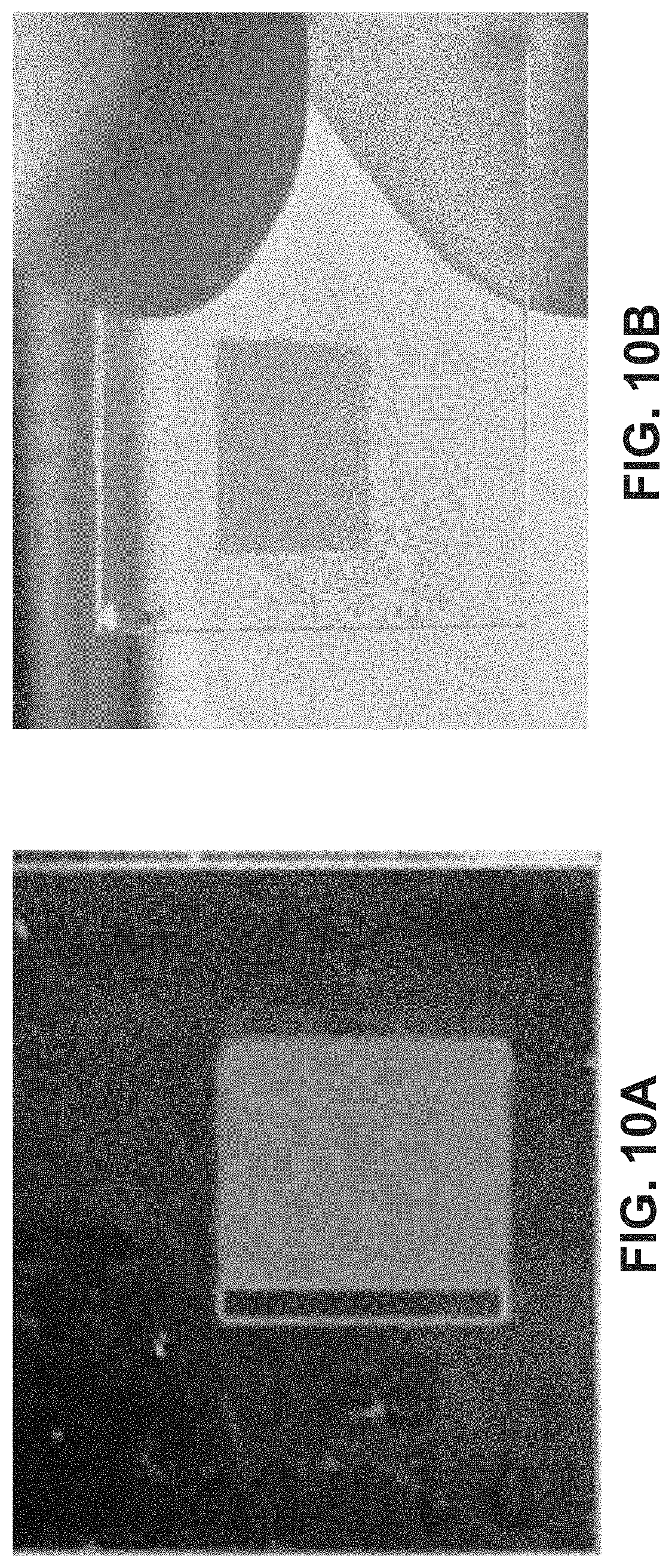
[0145] FIGS. 10A and 10B are images comparing an HPDLC Bragg grating and a polymer surface relief grating or evacuated Bragg grating.
[0146] FIGS. 11A and 11B are two plots comparing an HPDLC Bragg grating and a polymer surface relief grating or evacuated Bragg grating.
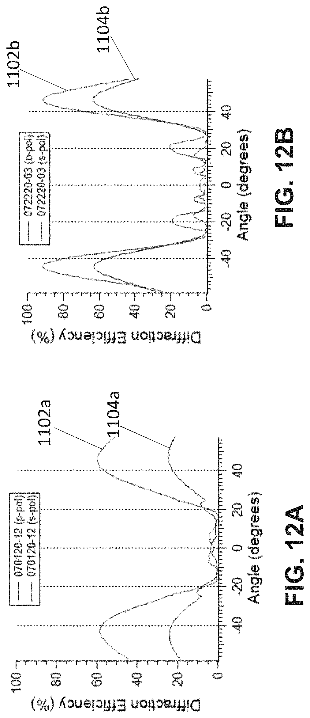
[0147] FIGS. 12A and 12B are two plots of S-diffraction efficiency and P-diffraction efficiency of two example polymer surface relief gratings with different depths.
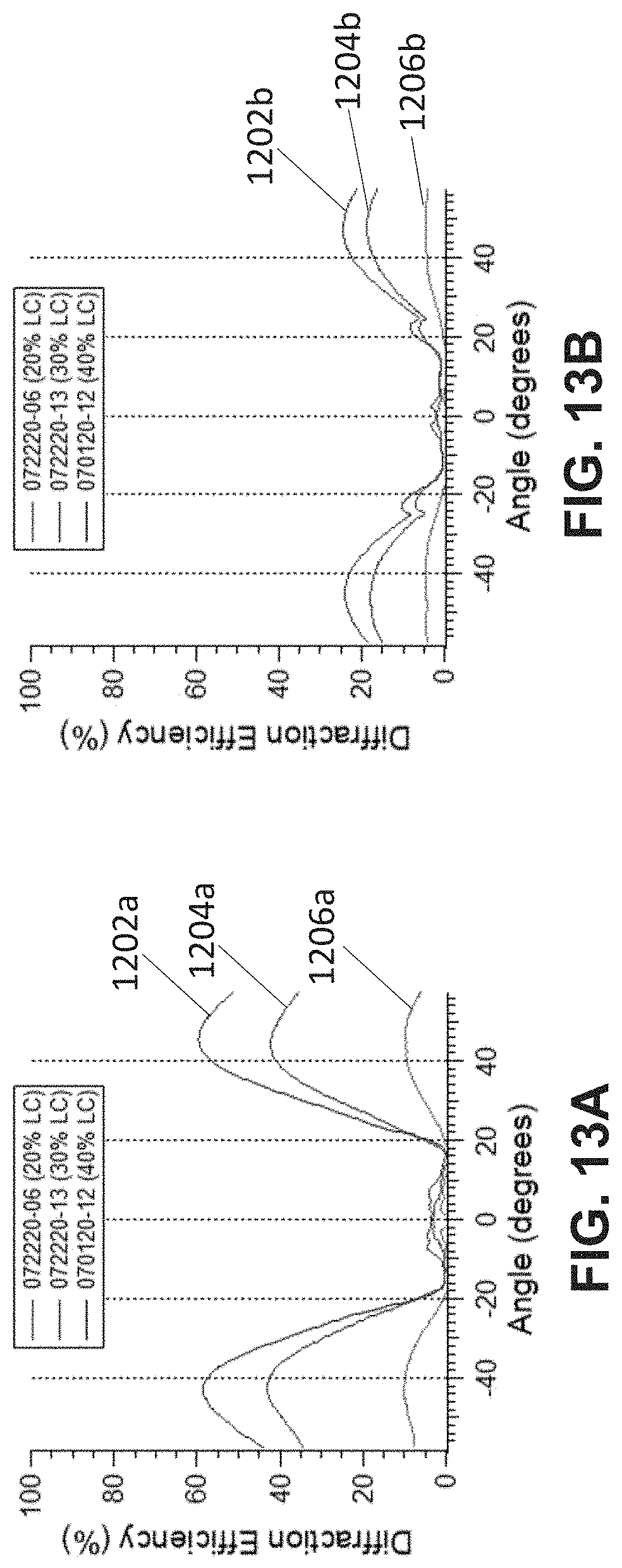
[0148] FIGS. 13A and 13B are two different plots of S-diffraction efficiency and P-diffraction efficiency of various example polymer surface relief gratings produced with different initial liquid crystal concentrations.
[0149] FIGS. 14A and 14B are two different plots of S-diffraction efficiency and P-diffraction efficiency of various example polymer surface relief gratings produced with different initial liquid crystal concentrations.
[0150] FIG. 15 conceptually illustrates a waveguide display in accordance with an embodiment of the invention.
[0151] FIG. 16 conceptually illustrates a waveguide display having two air-spaced waveguide layers in accordance with an embodiment of the invention.
[0152] FIG. 17 conceptually illustrates typical ray paths for a waveguide display in accordance with an embodiment of the invention.
[0153] FIG. 18 conceptually illustrates a waveguide display in which the waveguide supports a curved optical surface in accordance with an embodiment of the invention.
[0154] FIG. 19 conceptually illustrates a waveguide display in which the waveguide supports upper and lower curved optical surfaces in accordance with an embodiment of the invention.
[0155] FIG. 20 conceptually illustrates a waveguide display in which the waveguide supports a curved optical surface and an input image is provided using a pixel array predistorted to compensate for aberrations introduced by the curved optical surface in accordance with an embodiment of the invention.
[0156] FIG. 21 conceptually illustrates a waveguide display in which the waveguide supports a curved optical surface and an input image is provided using a pixel array supported by a curved substrate and predistorted to compensate for aberrations introduced by the curved optical surface in accordance with an embodiment of the invention.
[0157] FIG. 22 is a flow chart conceptually illustrating a method for projecting image light for view using a waveguide containing S-diffracting and P-diffracting gratings in accordance with an embodiment of the invention.
[0158] FIG. 23 is a flow chart conceptually illustrating a method for projecting image light for view using a waveguide supporting an optical prescription surface and containing S-diffracting and P-diffracting gratings in accordance with an embodiment of the invention.
[0159] FIG. 24A conceptually illustrates a portion of a pixel pattern having rectangular elements of differing size and aspect ratio for use in an emissive display panel in accordance with an embodiment of the invention.
[0160] FIG. 24B conceptually illustrates a portion of a pixel pattern having Penrose tiles for use in an emissive display panel in accordance with an embodiment of the invention.
[0161] FIG. 24C conceptually illustrates a portion of a pixel pattern having hexagonal elements for use in an emissive display panel in accordance with an embodiment of the invention.
[0162] FIG. 24D conceptually illustrates a portion of a pixel pattern having square elements for use in an emissive display panel in accordance with an embodiment of the invention.
[0163] FIG. 24E conceptually illustrates a portion of a pixel pattern having diamond-shaped elements for use in an emissive display panel in accordance with an embodiment of the invention.
[0164] FIG. 24F conceptually illustrates a portion of a pixel pattern having isosceles triangular elements for use in an emissive display panel in accordance with an embodiment of the invention.
[0165] FIG. 24G conceptually illustrates a portion of a pixel pattern having hexagonal elements with horizontally biased aspect ratios for use in an emissive display panel in accordance with an embodiment of the invention.
[0166] FIG. 24H conceptually illustrates a portion of a pixel pattern having rectangular elements with horizontally biased aspect ratios for use in an emissive display panel in accordance with an embodiment of the invention.
[0167] FIG. 24I conceptually illustrates a portion of a pixel pattern having diamond shaped elements with horizontally biased aspect ratios for use in an emissive display panel in accordance with an embodiment of the invention.
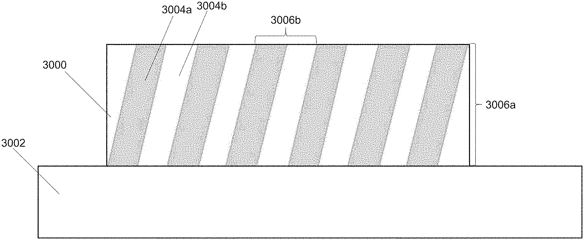
[0168] FIG. 24J conceptually illustrates a portion of a pixel pattern having triangles with horizontally biased aspect ratios for use in an emissive display panel in accordance with an embodiment of the invention.
[0169] FIG. 25 conceptually illustrates a portion of a pixel pattern having diamond shaped elements in which different pixels can have different emission characteristics in accordance with an embodiment of the invention.
DETAILED DESCRIPTION
[0170] There is a growing interest in the use of various gratings on waveguides in order to provide a variety of functions. These gratings include angle multiplexed gratings, color multiplexed gratings, fold gratings, dual interaction gratings, rolled K-vector gratings, crossed fold gratings, tessellated gratings, chirped gratings, gratings with spatially varying refractive index modulation, gratings having spatially varying grating thickness, gratings having spatially varying average refractive index, gratings with spatially varying refractive index modulation tensors, and gratings having spatially varying average refractive index tensors. In specific examples, gratings for diffraction of various polarizations of light (e.g. S-polarized light and P-polarized light) may be beneficial. It would be specifically advantageous to have a grating which diffracts either S-polarized light or P-polarized light. Specific applications for this technology include waveguide-based displays such as augmented reality displays and virtual reality displays. One example is input gratings which may be used to input one or both of S-polarized light or P-polarized light into the waveguide. However, in many cases, it would be advantageous to have a grating which diffracts either S-polarized light and P-polarized light. For example, waveguide displays using unpolarized light sources such as OLED light sources produce both S-polarized and P-polarized light and thus it would be advantageous to have gratings which can diffract both S-polarized and P-polarized light.
[0171] One specific class of gratings includes surface relief gratings (SRGs) which may be used to diffract either P-polarized light or S-polarized light. Another class of gratings are surface relief Bragg gratings (SBGs) which are normally P-polarization selective, leading to a 50% efficiency loss with unpolarized light sources such as organic light emitting diodes (OLEDs) and light emitting diodes (LEDs). Combining a mixture of S-polarization diffracting and P-polarization diffracting gratings may provide a theoretical 2.times. improvement over waveguides using P-diffracting gratings only. Thus, it would be advantageous to have a high efficiency S-polarization diffraction grating. In many embodiments, an S-polarization diffracting grating can be provided by a Bragg grating formed in a holographic photopolymer. In some embodiments, an S-polarization diffracting grating can be provided by a Bragg grating formed in a holographic polymer dispersed liquid crystal (HPDLC) with birefringence altered using an alignment layer or other processes for realigning the liquid crystal (LC) directors. In several embodiments, an S-polarization diffracting grating can be formed using liquid crystals, monomers, and other additives that naturally organize into S-diffracting gratings under phase separation. In some embodiments, these HPDLC gratings may form deep SRGs which have superior S-polarization diffraction efficiency.
[0172] One class of deep SRGs are polymer-air SRGs or evacuated Bragg gratings (EBGs) which may exhibit high S-diffraction efficiency (up to 99%) and low P-diffraction efficiency and may be implemented as input gratings for waveguides. Such gratings can be formed by removing the liquid crystal from SBGs formed from holographic phase separation of a liquid crystal and monomer mixture. Deep SRGs formed by such a process typically have a thickness in the range 1-3 micrometers with a Bragg fringe spacing 0.35 to 0.80 micrometers. In some embodiments, the ratio of grating depth to Bragg fringe spacing may be 1:1 to 5:1. As can readily be appreciated, such gratings can be formed with different dimensions depending on the specific requirements of the given application. Examples of how the thickness of SRGs may yield different resultant diffraction efficiencies are described in connection with FIGS. 6-8.
[0173] In many embodiments, the condition for a deep SRGs is characterized by a high grating depth to fringe spacing ratio. In some embodiments, the condition for the formation of a deep SRGs is that the grating depth is approximately twice the grating period. Modelling such deep SRGs using the Kogelnik theory can give reasonably accurate estimates of diffraction efficiency, avoiding the need for more advanced modelling, which typically entails the numerical solution of Maxwell's equations. The grating depths that can be achieved using liquid crystal removal from HPDLC gratings greatly surpass those possible using conventional nanoimprint lithographic methods, which cannot achieve the conditions for deep SRGs (typically providing only 250-300 nm depth for grating periods 350-460 nm). (Pekka Ayras, Pasi Saarikko, Tapani Levola, "Exit pupil expander with a large field of view based on diffractive optics", Journal of the SID 17/8, (2009), pp 659-664). It should be emphasized here that, although the S-polarization diffracting deep SRGs are emphasized within the present application, deep SRGs can, as will be discussed below, provide a range of polarization response characteristics depending on the thickness of the grating prescription and, in particular, the grating depth. As such, deep SRGs can be implemented in a variety of different applications.
[0174] The literature supports equivalence of deep SRGs and Bragg gratings. One reference (Kiyoshi Yokomori, "Dielectric surface-relief gratings with high diffraction efficiency" Applied Optics; Vol. 23; Issue 14; (1984); pp. 2303-2310), discloses the investigation of the diffraction properties of dielectric surface-relief gratings by solving Maxwell's equations numerically. The diffraction efficiency of a grating with a groove depth about twice as deep as the grating period was found to be comparable with the efficiency of a volume phase grating. The modelling by Yokomori predicted that dielectric surface-relief gratings interferometrically recorded in photoresist can possess a high diffraction efficiency of up to 94% (throughput efficiency 85%). The equivalence of deep SRGs and Bragg gratings is also discussed in another article by Golub (M. A. Golub, A. A. Friesem, L. Eisen "Bragg properties of efficient surface relief gratings in the resonance domain", Optics Communications; 235; (2004); pp 261-267). A further article by Gerritsen discusses the formation of Bragg-like SRGs in photoresist (Gerritsen H J, Thornton D K, Bolton S R; "Application of Kogelnik's two-wave theory to deep, slanted, highly efficient, relief transmission gratings" Applied Optics; Vol. 30; Issue 7; (1991); pp 807-814).
[0175] Many embodiments of this disclosure provide for methods of making SRGs such as deep SRGs that can offer very significant advantages over nanoimprint lithographic process particle for slanted gratings. Bragg gratings of any complexity can be made using interference or master and contact copy replication. In some embodiments, after removing the LC, the SRGs can be back filled with a material with different properties to the LC. This allows a Bragg grating with modulation properties that are not limited by the grating chemistry needed for grating formation.
[0176] In some embodiments the back fill material may not be a LC material. In some embodiments, the back fill material may have a higher index of refraction than air which may increase the angular bandwidth of a waveguide. In several embodiments, the deep SRGs can be partially backfilled with LC to provide a hybrid SRG/Bragg grating. Alternatively, in some embodiments, the refill step can be avoided by removing just a portion of the LC from the LC rich regions of the HPDLC to provide a hybrid SRG/Bragg grating. The refill approach has the advantage that a different LC can be used to form the hybrid grating. The materials can be deposited using an inkjet deposition process.
[0177] In some embodiments, the methods described herein may be used to create photonic crystals. Photonic crystals may be implemented to create a wide variety of diffracting structures including Bragg gratings. Bragg gratings may be used as diffraction gratings to provide functionality including but not limited to input gratings, output gratings, beam expansion gratings, diffract more than one primary color. A photonic crystal can be a three-dimensional lattice structure that can have diffractive capabilities not achievable with a basic Bragg grating. Photonic crystals can include many structures including all 2-D and 3-D Bravais lattices. Recording of such structures may benefit from more than two recording beams.
[0178] In some embodiments, waveguides incorporating photonic crystals can be arranged in stacks of waveguides, each having a grating prescription for diffracting a unique spectral bandwidth. In many embodiments, a photonic crystal formed by liquid crystal extraction provide a deep SRG. In many embodiments, a deep SRG formed using a liquid crystal extraction process can typically have a thickness in the range 1-3 micron with a Bragg fringe spacing 0.35 micron to 0.80 micron. In many embodiments, the condition for a deep SRG is characterized by a high grating depth to fringe spacing ratio. In some embodiments the condition for the formation of a deep SRG is that the grating depth can be approximately twice the grating period. It should be emphasized here that, although S-polarization diffracting deep SRGs are of main interest in the present application, deep SRGs can, as will be discussed below, provide a range of polarization response characteristics depending on the thickness of the grating prescription and, in particular, the grating depth. Deep SRGs can also be used in conjunction with conventional Bragg gratings to enhance the color, uniformity and other properties of waveguide displays.
[0179] Deep SRGs have been fabricated in glassy monomeric azobenzene materials using laser holographic exposure (O. Sakhno, L. M. Goldenberg, M. Wegener, J. Stumpe, "Deep surface relief grating in azobenzene-containing materials using a low intensity 532 nm laser", Optical Materials: X, 1, (2019), 100006, pp 3-7. The Sakhno reference also discloses how SRGs can be recorded in a holographic photopolymer using two linearly orthogonally polarized laser beams.
[0180] The disclosure provides a method for making a surface relief grating that can offer very significant advantages over nanoimprint lithographic process particularly for slanted gratings. Bragg gratings of any complexity can be made using interference or master and contact copy replication. In some embodiments after removing the LC the SRG can be back filled with a material with different properties to the LC. This allows a Bragg grating with modulation properties that are not limited by the grating chemistry needed for grating formation. In some embodiments the SRGs can be partially backfilled with LC to provide a hybrid SRG/Bragg grating. Alternatively, in some embodiments, the refill step can be avoided by removing just a portion of the LC from the LC rich regions of the HPDLC to provide a hybrid SRG/Bragg grating. The refill approach has the advantage that a different LC can be used to form the hybrid grating. The materials can be deposited using an inkjet process as disclosed in earlier filings by the inventors. In some embodiments, the refill material may have a higher index of refraction than air which may increase diffraction efficiency of the grating.
[0181] While this disclosure has been made in the context of fabricating deep SRGs, it is appreciated that many other grating structures may be produced using the techniques described herein. For example, any type of SRG including SRGs in which the grating depth is smaller than the grating frequency (e.g. Raman-Nath gratings) may be fabricated as well.
[0182] FIGS. 1A-1D illustrate a processing apparatus that can be used in a method for fabricating deep SRGs or EBGs in accordance with an embodiment. FIG. 1A conceptually illustrates an apparatus 190A that can be used in a step of a method for fabricating a surface relief grating in which a mixture 191 of monomer and liquid crystal deposited on a transparent substrate 192 is exposed to holographic exposure beams 193,194, in accordance with an embodiment of the invention. In some examples, the mixture may also include at least one of a photoinitiator, a coinitiator, a multifunctional thiol, adhesion promoter, surfactant, and/or additional additives. In some embodiments, the monomer may be isocyanate-acrylate based or thiolene based. In some embodiments, the liquid crystal may be a full liquid crystal mixture or a liquid crystal single only including a portion of a full liquid crystal mixture. Various examples of liquid crystal singles include one or both of cyanobiphenyls or pentylcyanobiphenyls. In some embodiments, liquid crystal may be replaced with another substance that phase separates with the monomer during exposure to create polymer rich regions and substance rich regions. Advantageously, the substance and liquid crystal singles may be a cost-effective substitute to full liquid crystal mixtures which are removed at a later step as described below.
[0183] FIG. 1B conceptually illustrates an apparatus 190B that can be used in a step of a method for fabricating a surface relief grating from an HPDLC Bragg grating 195 formed on a transparent substrate using the holographic exposure beams, in accordance with an embodiment of the invention. The holographic exposure beams may transform the monomer into a polymer in some areas. The holographic exposure beams may include intersecting recording beams and include alternating bright and dark illumination regions. A polymerization-driven diffusion process may cause the diffusion of monomers and LC in opposite directions, with the monomers undergoing gelation to form polymer-rich regions (in the bright regions) and the liquid crystal becoming trapped in a polymer matrix to form liquid crystal rich regions (in the dark regions).
[0184] FIG. 1C conceptually illustrates an apparatus 190C that can be used in a step of a method for fabricating a deep polymer surface relief grating 196 or EBG in which liquid crystal is removed from an HPDLC Bragg grating of FIG. 1B to form a polymer surface relief grating in accordance with an embodiment of the invention. Advantageously, a polymer surface relief grating 196 may include a large depth with a comparatively small grating period in order to form a deep SRG. The liquid crystal may be removed by washing with a solvent such as isopropyl alcohol (IPA). The solvent should be strong enough to wash away the liquid crystal but weak enough to maintain the polymer. In some embodiments, the solvent may be chilled below room temperature before washing the grating. FIG. 1D conceptually illustrates an apparatus 190D that can be used in a step of a method for fabricating a polymer surface relief grating in which the polymer surface relief grating is covered with a protective layer 197 in accordance with an embodiment of the invention.
[0185] FIG. 2 conceptually illustrates a method for forming deep SRGs from a HPDLC Bragg grating formed on a transparent substrate in accordance with an embodiment. As shown, the method 200 of forming deep SRGs or EBGs is provided. Referring to the flow diagram, the method 200 includes providing (201) a mixture of at least one monomer and at least one liquid crystal. The at least one monomer may include an isocyanate-acrylate monomer or thiolene. In some embodiments, the at least one liquid crystal may be a full liquid crystal mixture or may be a liquid crystal single which may include only a portion of the liquid crystal mixture such as a single component of the liquid crystal mixture. In some embodiments, the at least one liquid crystal may be substituted for a solution which may phase separate with the monomer during exposure. The criteria for such a solution may include ability to phase separate with the monomer during exposure, ease of removal after curing and during washing, and ease of handing. Example substitute solutions include solvents, non-reactive monomers, inorganics, and nanoparticles.
[0186] Providing the mixture of the monomer and the liquid crystal may also include mixing one or more of the following with the at least one monomer and the liquid crystal: initiators such as photoinitiators or coinitiators, multifunctional thiol, dye, adhesion promoters, surfactants, and/or additional additives such as other cross linking agents. This mixture may be allowed to rest in order to allow the coinitiator to catalyze a reaction between the monomer and the thiol. The rest period may occur in a dark space or a space with red light (e.g. infrared light) at a cold temperature (e.g. 20.degree. C.) for a period of approximately 8 hours. After resting, additional monomers may be mixed into the monomer. This mixture may be then strained or filtered through a filter with a small pore size (e.g. 0.45 .mu.m pore size). After straining, this mixture may be stored at room temperature in a dark space or a space with red light before coating.
[0187] Next, a transparent substrate can be provided (202). In certain embodiments, the transparent substrate may be a glass substrate or a plastic substrate. A layer of the mixture can be deposited or coated (203) onto a surface of the substrate. In some embodiments, the mixture is sandwiched between the transparent substrate and another substrate using glass spacers to maintain internal dimensions. A non-stick coating may be applied to the other substrate before the mixture is sandwiched. The non-stick coating may include a fluoropolymer such as OPTOOL UD509 (produced by Daikin Chemicals), Dow Corning 2634, Fluoropel (produced by Cytonix), and EC200 (produced by PPG Industries, Inc). Holographic recording beams can be applied (204) to the mixture layer. The holographic recording beams may be a two-beam interference pattern which may cause phase separation of the LC and the polymer. In response to the holographic recording beam, the liquid monomer changes to a solid polymer whereas the neutral, non-reactive substance (e.g. LC) diffuses during holographic exposure in response to a change in chemical potential driven by polymerization. While LC may be one implementation of the neutral, non-reactive substance, other substances may also be used. The substance and the monomer may form a miscible mixture prior to the holographic exposure and become immiscible upon holographic exposure.
[0188] After applying the holographic recording beams, the mixture may be cured. The curing process may include leaving the mixture under low-intensity white light for a period of time until the mixture fully cures. The low intensity white light may also cause a photo-bleach dye process to occur. Thus, a HPDLC grating having alternating polymer rich and liquid crystal rich regions can be formed (205). In some embodiments, the curing process may occur in two hours or less. After curing, one of the substrates may be removed exposing the HPDLC grating. Advantageously, the non-stick coating may allow the other substrate to be removed with the HPDLC grating remaining.
[0189] HPDLC grating may include alternating sections of liquid crystal rich regions and polymer regions. The liquid crystal in the liquid crystal rich regions can be removed (206) to form polymer surface relief gratings or EBGs which may be used as deep SRGs. The liquid crystal may be removed by gently immersing the grating into a solvent such as IPA. The IPA may be chilled and may be kept at a temperature lower than room temperature while the grating is immersed in the IPA. The grating is then removed from the solvent and dried. In some embodiments, the grating is dried using a high flow air source such as compressed air. After the LC is removed from the grating, a polymer-air surface relief Bragg grating is formed.
[0190] As shown in FIGS. 1A-1D, the formed surface relief grating can further be covered with a protective layer. In some instances, the protective layer may be a moisture and oxygen barrier with scratch resistance capabilities. In some instances, the protective layer may be a coating that does not fill in air gap regions where LC that was removed once existed. The coating may be deposited using a low temperature process. In some implementations, the protective layer may have anti-reflective (AR) properties. The coating may be a silicate or silicon nitride. The coating process may be preformed by a plasma assisted chemical vapor deposition (CVD) process such as a nanocoating process. The coating may be a parylene coating. The protective layer may be a glass layer. A vacuum or inert gas may fill the gaps where LC that was removed once existed before the protective layer is implemented. In some embodiments, the coating process may be integrated with the LC removal process (206). For example, a coating material may be mixed with the solvent which is used to wash the LC from the grating.
[0191] FIG. 3 illustrates a cross sectional schematic view of an exemplary embodiment of a polymer-air surface relief Bragg grating 3000 implemented on a waveguide 3002. The polymer-air surface relief Bragg grating 3000 includes periodic polymer sections 3004a. Adjacent polymer sections sandwich air sections 3004b. The air sections 3004b are sandwiched by polymer sections 3004a. The air sections 3004b and polymer sections 3004a have different indexes of refraction. Advantageously, the polymer-air surface relief Bragg grating 3000 may be formed with a high grating depth 3006a to Bragg fringe spacing 3006b ratio which may create a deep SRG. As discussed previously, deep SRGs may exhibit many beneficial qualities such as high S-diffraction efficiency which may not be present within the typical SRGs.
[0192] In one example, a polymer-air surface relief Bragg grating 3000 may have a Bragg fringe spacing 3006b of 0.35 .mu.m to 0.8 .mu.m and a grating depth of 1 .mu.m to 3 .mu.m. In some embodiments, the polymer sections 3004a may include at least some residual liquid crystal when the liquid crystal is not completely removed during step 206 described in connection with FIG. 2. In some embodiments, the presence of residual LC within the polymer rich regions may increase refractive index modulation of the final polymer SRG. In some embodiments, the air sections 3004b may include some residual liquid crystal if the liquid crystal is not completely removed during step 206 from these air sections 3004b. In some embodiments, by leaving some residual liquid crystal within the air sections 3004b, a hybrid grating as described in connection with FIGS. 4-5 may be created.
[0193] As discussed above, in many the embodiments, the invention also provides a method for fabricating a hybrid surface relief/Bragg grating. FIG. 4A conceptually illustrates an apparatus 210A that can be used in a step of a method for fabricating hybrid surface relief gratings (hybrid SRGs) in which a mixture 211 of monomer and liquid crystal deposited on a transparent substrate 212 is exposed to holographic exposure beams 213,214, in accordance with an embodiment of the invention. FIG. 4B conceptually illustrates an apparatus 210B that can be used in a step of a method for fabricating hybrid SRGs from an HPDLC Bragg grating 215 formed on the transparent substrate using the holographic exposure beams in accordance with an embodiment of the invention. FIG. 4C conceptually illustrates an apparatus 210C that can be used in a step of a method for fabricating a surface relief grating in which liquid crystal is removed from an HPDLC Bragg grating to form polymer-air SRGs 216 in accordance with an embodiment of the invention. These polymer-air SRGs 216 or EBGs may be deep SRGs. It is appreciated that the steps illustrated in and described in connection with FIGS. 4A-4C roughly correspond to the steps illustrated in and described in connection with FIGS. 2A-2C in the process to create a polymer-air SRG and thus the previous description will be applicable to FIGS. 4A-4C.
[0194] In addition, FIG. 4D conceptually illustrates an additional step which may be performed to create a hybrid grating. The apparatus 210D can be used in a step of a method for fabricating a surface relief grating in which a surface relief grating is at least partially refilled with liquid crystal to form a hybrid SRGs 217, in accordance with an embodiment of the invention. The refilled liquid crystal may be of different consistency to the previously removed liquid crystal that was previously removed in FIG. 4C. Further, it is appreciated that the liquid crystal removed in FIG. 3C may only be partially removed in an alternative method to forming hybrid SRGs 217. In addition, FIG. 4E conceptually illustrates an apparatus 210E can be used in a step of a method for fabricating a surface relief grating in which hybrid SRGs 217 formed in the step illustrated in FIG. 4D is covered with a protective layer 218, in accordance with an embodiment of the invention.
[0195] FIG. 5 is a flowchart showing an exemplary method for forming a hybrid surface relief-Bragg grating from a HPDLC Bragg grating formed on a transparent substrate in accordance with an embodiment of the invention. As shown, the method 220 of forming hybrid surface relief-Bragg grating is provided. Referring to the flow diagram, method 220 includes providing (221) a mixture of at least one monomer and at least one liquid crystal. The at least one monomer may include an isocyanate-acrylate monomer. Providing the mixture of the monomer and the liquid crystal may also include mixing one or more of the following with the at least one monomer and the liquid crystal: photoinitiator, coinitiator, multifunctional thiol, and/or additional additives. This mixture may be allowed to rest in order to allow the coinitiator to catalyze a reaction between the monomer and the thiol. The rest period may occur in a dark space or a space with red light (e.g. infrared light) at a cold temperature (e.g. 20.degree. C.) for a period of approximately 8 hours. After resting, additional monomers may be mixed into the monomer. This mixture may be then strained or filtered through a filter with a small pore size (e.g. 0.45 .mu.m pore size). After straining this mixture may be stored at room temperature in a dark space or a space with red light before coating.
[0196] Next, a transparent substrate can be provided (222). In certain embodiments, the transparent substrate may be a glass substrate or a plastic substrate. A non-stick coating may be applied to the transparent substrate before the mixture is coated on the substrate. A layer of the mixture can be deposited (223) onto a surface of the substrate. In some embodiments, the mixture is sandwiched between the transparent substrate and another substrate using glass spacers to maintain internal dimensions. Holographic recording beams can be applied (224) to the mixture layer. The holographic recording beams may be a two-beam interference pattern which may cause phase separation of the LC and the polymer. After applying the holographic recording beams, the mixture may be cured. The curing process may include leaving the mixture under low-intensity white light for a period of time under the mixture fully cures. The low intensity white light may also cause a photo-bleach dye process to occur. Thus, an HPDLC grating having alternating polymer rich and liquid crystal rich regions can be formed (225). In some embodiments, the curing process may occur in 2 hours or less. After curing, one of the substrates may be removed exposing the HPDLC grating.
[0197] HPDLC grating may include alternating sections of liquid crystal rich regions and polymer regions. The liquid crystal in the liquid crystal rich regions can be removed (226) to form polymer surface relief gratings or EBGs which is a form of deep SRGs. The liquid crystal may be removed by gently immersing the grating into a solvent such as isopropyl alcohol (IPA). The IPA may be kept at a lower temperature while the grating is immersed in the IPA. The grating is them removed from the solvent and dried. In some embodiments, the grating is dried using a high flow air source such as compressed air. After the LC is removed from the grating, a polymer-air surface relief Bragg grating is formed. The steps 221-226 of FIG. 5 roughly correspond to the steps described in connection with FIG. 2 in creating a polymer-air SRG and thus these descriptions are applicable to FIG. 5.
[0198] Further, method 220 includes at least partially refilling (227) cleared liquid crystal rich regions with liquid crystal to form hybrid SRGs. The refilled liquid crystal may be of different consistency to the previously removed liquid crystal that was previously removed in step 226. Further, it is appreciated that the liquid crystal removed in step 226 may only be partially removed in an alternative method to forming hybrid SRGs. Advantageously, hybrid SRGs may provide the ability to tailor specific beneficial characteristics of the SRGs. One particular characteristic that may be improved by the inclusion of at least some liquid crystal within the SRGs is a decrease in haze properties.
[0199] As shown in FIG. 4E, the formed surface relief grating can further be covered with a protective layer. In some instances, the protective layer may be a moisture and oxygen barrier with scratch resistance capabilities. In some instances, the protective layer may be a coating that does not fill in air gap regions where LC that was removed once existed. The coating may be deposited using a low temperature process. In some implementations, the protective layer may have anti-reflective (AR) properties. The coating may be a silicate or silicon nitride. The coating process may be preformed by a plasma assisted chemical vapor deposition (CVD) process such as a plasmatreat nanocoating process. The coating may be a parylene coating. The protective layer may be a glass layer. A vacuum or inert gas may fill the gaps where LC that was removed once existed before the protective layer is implemented. In some embodiments, the coating process may be integrated with the LC removal process (226). For example, a coating material may be mixed with the solvent which is used to wash the LC from the grating. In some implementations, the coating material may be a material with a lower or higher refractive index than the polymer and fill the spaces between adjacent polymer portions. The refractive index difference between the polymer and the coating material may allow the polymer SRGs to continue to diffract.
[0200] Although FIGS. 1-5 illustrate specific methods and apparatus for forming deep SRGs and hybrid surface relief/Bragg gratings, various manufacturing methods implementing different steps or modifications of such steps can be utilized. As can readily be appreciated, the specific process utilized can depend on the specific requirements of the given application. For example, many embodiments utilize another grating as a protective layer.
[0201] Hybrid SRG/Bragg gratings with shallow SRG structures may lead to low SRG diffraction efficiencies. The methods disclosed in the present disclosure allows for more effective SRG structures to be formed by optimizing the depth of the liquid crystal in the liquid crystal rich regions such that the SRGs has a high depth to grating pitch ratio while allowing the Bragg grating to be sufficiently thick for efficient diffraction. In many embodiments, the Bragg grating component of the hybrid grating can have a thickness in the range 1-3 micrometer. In some embodiments, the SRG component of the hybrid grating can have a thickness in the range 0.25-3 micrometer. The initial HPDLC grating would have a thickness equal to the sum of the final SRG and Bragg grating components. As can readily be appreciated, the thickness ratio of the two grating components can depend on the waveguide application. In some embodiments, the combination of an SRG with a Bragg grating may be used to fine-tune angular bandwidth of the grating structure. In some cases, the SRG can increase the angular bandwidth of the grating structure.
[0202] In many embodiments, in the hybrid SRGs illustrated in FIGS. 4A-4E, the refill depth of the liquid crystal regions of the grating can be varied across the grating to provide spatially varying relative SRG/Bragg grating strengths. In some embodiments, during the liquid crystal removal and refill as defined in steps 206, 226, and 227, the liquid crystal in the liquid crystal rich grating regions can be totally or partially removed. In several embodiments, the liquid crystal used to refill or partially refill the liquid crystal-cleared regions can have a different chemical composition to the liquid crystal used to form the initial HPDLC grating. In various embodiments, a first liquid crystal with phase separation properties compatible with the monomer can be specified to provide a HPDLC grating with optimal modulation and grating definitions while a second refill liquid crystal can be specified to provide desired index modulation properties in the final hybrid grating. In a number of embodiments, the Bragg portion of the hybrid grating can be switchable with electrodes applied to surfaces of the substrate and the cover layer. In many embodiments, the refill liquid crystals can contain additives which may include but are not limited to the features of improving switching voltage, switching time, polarization, transparency, and other parameters. A hybrid grating formed using a refill process would have the further advantages that the LC would form a continuum (rather than an assembly of LC droplets), thereby reducing haze.
[0203] While deep SRGs, EBGs, and/or hybrid SRGs may be described in the context of S-diffracting gratings and P-diffracting gratings, these gratings have applicability in many other grating types. These include but are not limited to angle multiplexed gratings, color multiplexed gratings, fold gratings, dual interaction gratings, rolled K-vector gratings, crossed fold gratings, tessellated gratings, chirped gratings, gratings with spatially varying refractive index modulation, gratings having spatially varying grating thickness, gratings having spatially varying average refractive index, gratings with spatially varying refractive index modulation tensors, and gratings having spatially varying average refractive index tensors. Further, deep SRGs, EBGs, and/or hybrid SRGs may be switchable or non-switchable gratings depending on their specific implementation. Deep SRGs, EBGs, and/or hybrid SRGs may be fabricated on a plastic substrate or a glass substrate. These gratings may also be fabricated on one substrate and transferred to another substrate.
Discussion of Various Implementations of Deep SRGs or EBGs
[0204] In many embodiments, deep SRGs can provide a means for controlling polarization in a waveguide. SBGs are normally P-polarization selective, leading to a 50% efficiency loss with unpolarized light sources such as OLEDs and LEDs. Hence, combining S-polarization diffracting and P-polarization diffracting gratings can provide a theoretical 2.times. improvement over waveguides using P-diffracting gratings only. In some embodiments, an S-polarization diffracting grating can be provided by a Bragg grating formed in a conventional holographic photopolymer. In some embodiments an S-polarization diffracting grating can be provided by a Bragg grating formed in a HPDLC with birefringence altered using an alignment layer or other process for realigning the liquid crystal directors. In some embodiments, an S-polarization diffracting grating can be formed using liquid crystals, monomers and other additives that naturally organize into S-diffracting gratings under phase separation. In many embodiments, an S-polarization diffracting grating can be provided by SRGs. Using the processes described above, a deep SRG exhibiting high S-diffraction efficiency (up to 99%) and low P-diffraction efficiency can be formed by removing the liquid crystal from SBGs formed from holographic phase separation of a liquid crystal and monomer mixture.
[0205] Deep SRGs can also provide other polarization response characteristics. Several prior art theoretical studies such as an article by Moharam (Moharam M. G. et al. "Diffraction characteristics of photoresist surface -relief gratings", Applied Optics, Vol. 23, page 3214, Sep. 15, 1984) point to deep surface relief gratings having both S and P sensitivity with S being dominant. In some embodiments, deep SRGs demonstrate the capability of providing an S-polarization response. However, deep SRGs may also provide other polarization response characteristics. In many embodiments, deep surface relief gratings having both S and P sensitivity with S being dominant are implemented. In some embodiments, the thickness of the SRG can be adjusted to provide a variety of S and P diffraction characteristics. In several embodiments, diffraction efficiency can be high for P across a spectral bandwidth and angular bandwidth and low for S across the same spectral bandwidth and angular bandwidth. In number of embodiments, diffraction efficiency can be high for S across the spectral bandwidth and angular bandwidth and low for P across the same spectral bandwidth and angular bandwidth. In some embodiments, high efficiency for both S and P polarized light can be provided. A theoretical analysis of an SRG of refractive index 1.6 immersed in air (hence providing an average grating index of 1.3) of period 0.48 micron, with a 0 degrees incidence angle and 45 degree diffracted angle for a wavelength of 0.532 micron is shown in FIGS. 5-7. FIG. 5 is a graph showing calculated P-polarized and S-polarized diffraction efficiency versus incidence angle for a 1-micrometer thickness deep surface relief grating, demonstrating that in this case high S and P response can be achieved. FIG. 6 is a graph showing calculated P-polarized and S-polarized diffraction efficiency versus incidence angle for a 2-micrometer thickness deep surface relief grating, demonstrating that in this case the S-polarization response is dominant over most of the angular range of the grating. FIG. 7 is a graph showing calculated P-polarized and S-polarized diffraction efficiency versus incidence angle for a 3-micrometer thickness, demonstrating that in this case the P-polarization response is dominant over a substantial portion of the angular range of the grating.
[0206] In many embodiments, a photonic crystal can be a reflection Bragg grating or deep SRG formed by a LC extraction process. A reflection deep SRG made using phase separation followed by LC subtraction can enable wide angular and spectral bandwidth. In many embodiments replacing the current input SBG with a reflection photonic crystal can be used to reduce the optical path from a picture generation unit (PGU) to a waveguide. In some embodiments, a PGU pupil and the waveguide can be in contact. In many embodiments, the reflection deep SRG can be approximately 3 microns in thickness. The diffracting properties of an LC extracted Bragg grating mainly result from the index gap between the polymer and air (not from the depth of the grating as in the case of a typical SRG).
Discussion of Thiol Additives within Initial Mixture
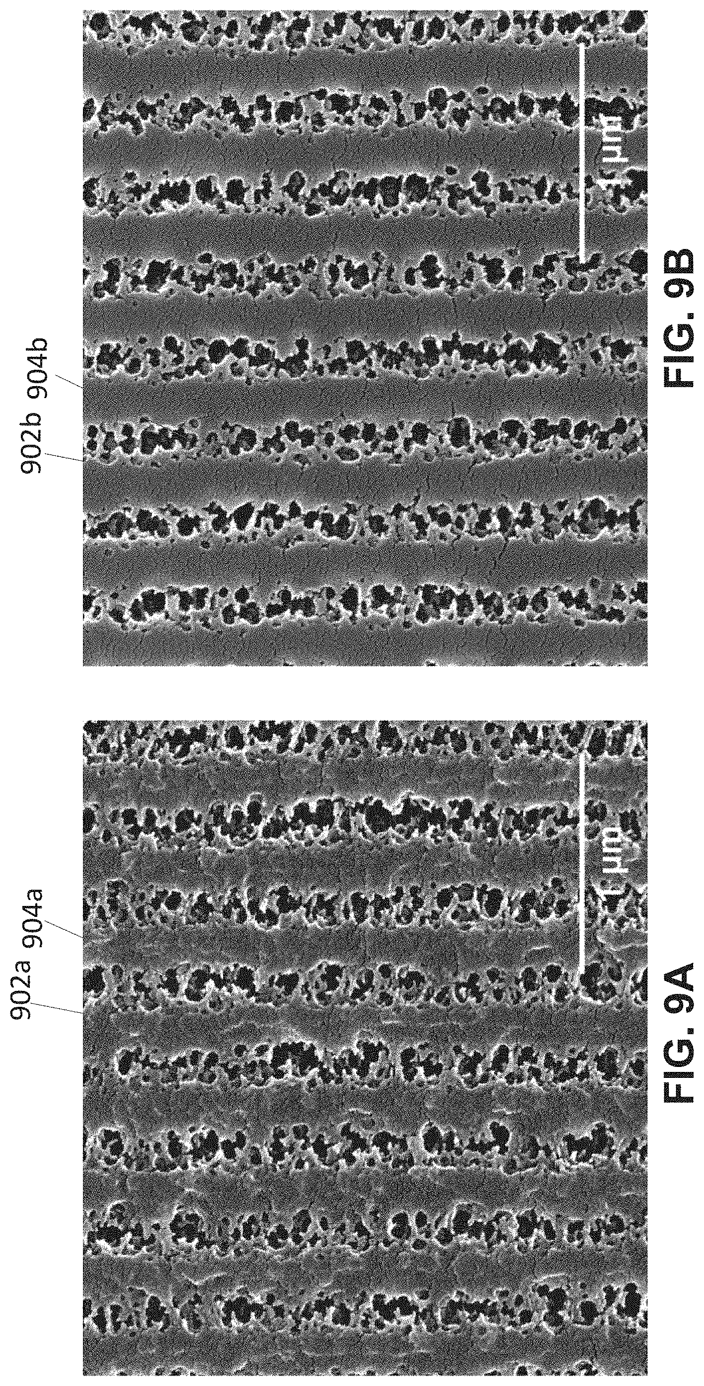
[0207] FIGS. 9A and 9B illustrate comparative scattering electron microscopy (SEM) images of example mixtures used to fabricate polymer-air SRGs. As discussed previously, the monomer within the initial mixture may be acrylate or thiolene based. It has been discovered that with some monomers such as acrylate based monomers, after holographic exposure, during washing, the solvent not only removes liquid crystal material but also polymer which is unideal. It has been discovered that a multifunctional thiol additive may solve this issue by strengthening the polymer and thus allowing it to be strong enough to withstand the solvent wash. Without limiting to any particular theory, thiol additive may improve the mechanical strength of formulations consisting of low functionality acrylate monomers which tend to form mechanically weak polymers due to reduced cross-linking. Acrylate monomer formulations may be advantageous because they may exhibit high diffraction efficiency with lower haze. Thus, adding thiol could allow Acrylate monomer formations to be a viable option in fabrication of polymer SRGs.
[0208] There may be a trade-off between phase separation, grating formation, and mechanical strength between different formulations. Grating formation may benefit from mixtures that contain low functionality monomers that react slower, form fewer cross-linkages, and allow greater diffusion of non-reactive components (e.g. LC) during holographic exposure. Conversely, mixtures consisting of high functionality monomers may exhibit better phase separation and polymer mechanical strength due to greater cross-linking, but may react so rapidly that the non-reactive components do not have sufficient time to diffuse and thus may exhibit lower diffraction efficiency as a result.
[0209] Without limitation to any particular theory, the thiol additives may get around these limitations by reacting with acrylates or isocyanate-acrylates to form a loose scaffolding prior to holographic exposure. This scaffolding may improve the mechanical strength and uniformity of the cured polymer. Thus, the mechanical strength may be tuned through slight adjustments of the thiol functionality and concentration without significantly raising the average functionality of the monomer mixture and disrupting grating formation.
[0210] FIG. 9A illustrates an initial mixture whereas FIG. 9B illustrate a comparative mixture which includes 1.5 wt % thiol. However, other weight percentages of thiol additive have been contemplated. For example, a weight percentage of thiol additive may be 1 to 4% or 1.5% to 3%. In some embodiments, the multifunctional thiol may be trimethylolpropane tris(3-mercaptopropionate). Both FIGS. 9A and 9B include polymer dense regions 902a/902b and air regions 904a/904b. As illustrated, the added thiol may produce a denser polymer structure within the polymer dense regions 902a of FIG. 9B than the polymer dense regions 902b of FIG. 9A which may increase grating performance. It has been discovered that the weight percentage of thiol additive should be balanced in order to provide stability within the polymer structure to withstand the solvent wash however not to be rigid as to not allow the liquid crystal to be released during the solvent wash.
Comparison between HPDLC Grating Performance with Polymer-Air SRG Performance
[0211] FIGS. 10A and 10B illustrates images of comparative examples of an HPDLC grating and a polymer SRG or EBG. FIG. 10A illustrates performance for an example HPDLC grating where liquid crystal has not been removed. The grating of FIG. 10A includes a 20-30% P-diffraction efficiency while exhibiting a nominal or almost 0% 5-diffraction efficiency. FIG. 10B illustrates performance of an example polymer-air SRG where the LC has been removed. The grating of FIG. 10B includes a 18-28% P-diffraction efficiency while exhibiting a S-diffraction efficiency of 51-77%. Thus, polymer-air SRGs where LC has been removed demonstrate a comparatively high S-diffraction efficiency while maintaining a comparable P-diffraction efficiency. Further, the grating of FIG. 10B includes a P-diffraction haze of 0.11-0.15% and a S-diffraction haze of 0.12-0.16%.
[0212] FIGS. 11A and 11B illustrates plots of comparative examples of an HPDLC grating where liquid crystal has not been removed and a polymer SRG or EBG where liquid crystal has been removed. FIG. 11A illustrates the P-diffraction efficiency and 5-diffraction efficiency for an HPDLC grating where liquid crystal remains. A first line 1102a corresponds to P-diffraction efficiency and a second line 1104a corresponds to S-diffraction efficiency. FIG. 11B illustrates the P-diffraction efficiency and S-diffraction efficiency for a polymer SRG or EBG where liquid crystal has been removed. A first line 1102b corresponds to P-diffraction efficiency and a second line 1104b corresponds to S diffraction efficiency. As illustrated, S-diffraction efficiency dramatically increases after liquid crystal has been removed while P-diffraction efficiency remains relatively similar.
[0213] In some embodiments, the ratio of S-diffraction efficiency to P-diffraction efficiency may be adjusted by using different grating periods, grating slant angles, and grating thicknesses.
Various Example Deep SRG Depths
[0214] FIGS. 12A and 12B illustrate various comparative examples of P-diffraction and S-diffraction efficiencies with deep SRGs of various depths. Each of these plots show diffraction efficiency vs. angle. In FIG. 12A, the deep SRG has a depth of approximately 1.1 .mu.m. The first line 1102a represents S-diffraction efficiency and the second line 1104a represents P-diffraction efficiency. As illustrated the peak S-diffraction efficiency is approximately 58% and the peak P-diffraction efficiency is 23%. It is noted that the haze for S-diffraction is 0.12% and haze for P-diffraction is 0.11% for this example. Such high diffraction efficiency with low haze may make deep SRGs with a depth of approximately 1.1 .mu.m particularly suitable for multiplexed gratings.
[0215] In FIG. 12B, the deep SRG has a depth of approximately 1.8 .mu.m. The first line 1102b represents S-diffraction efficiency and the second line 1104b represents P-diffraction efficiency. As illustrated the peak S-diffraction efficiency is approximately 92% and the peak P-diffraction efficiency is 63%. It is noted that the haze for S-diffraction is 0.34% and haze for P-diffraction is 0.40% for this example. Thus, both S-diffraction and P-diffraction efficiency increase dramatically with an increased grating depth. It is noted that haze appears to increase with the increased grating depth.
Various Example Initial LC Concentrations in Mixture
[0216] FIGS. 13A and 13B illustrate the results of a comparative study of various EBGs with various initial LC concentrations in the initial mixture. FIG. 13A illustrates S-diffraction efficiency vs. angle. FIG. 13B illustrates P-diffraction efficiency vs. angle. In FIG. 13A, a first line 1202a corresponds to 20% initial LC content, a second line 1204a corresponds to 30% initial LC content, and a third line 1206a corresponds to 40% initial LC content. In FIG. 13B, a first line 1202b corresponds to 20% initial LC content, a second line 1204b corresponds to 30% initial LC content, and a third line 1206b corresponds to 40% initial LC content. Table 1 illustrates a summary of various results of the comparative study.
TABLE-US-00001 TABLE 1 Initial LC Maximum Maximum Content in S-Diffraction P-Diffraction S-Diffraction P-Diffraction Mixture Efficiency Efficiency Haze Haze 20% .sup. 10% 5% 0.10% 0.12% 30% .gtoreq.40% 18% 0.14% 0.13% 40% .gtoreq.55% 23% 0.12% 0.11%
[0217] As is illustrated in FIGS. 13A and 13B and noted in Table 1, the maximum S-diffraction and maximum P-diffraction appear to both increase with higher initial LC content while the S-diffraction haze and P-diffraction haze stay approximately constant.
[0218] FIGS. 14A and 14B illustrate additional example S-diffraction and P-diffraction efficiencies for various initial LC concentrations. FIG. 14A illustrates S-diffraction efficiency for various example EBGs including various initial LC contents. FIG. 14B illustrate P-diffraction efficiency for various example EBGs including various LC contents. For both FIG. 14A and 14B, sequentially from top to bottom the lines represent: 32% LC content, 30% LC content, 28% LC content, 26% LC content, 24% LC content, 22% LC content, and 20% LC content. As illustrated, the S-diffraction and P-diffraction efficiencies are directly related to the amount of LC content (e.g. higher LC content yields higher S-diffraction and P-diffraction efficiencies).
[0219] Without being limited to any particular theory, the initial LC content relates to amount of phase separation between the LC and the monomer that occurs during the holographic exposure process and polymerization process. Thus, a higher LC content will increase the amount of LC rich regions which are removed to make more air regions after washing. The increased air regions make greater refractive index differences (.DELTA.n) between the air regions (formerly liquid crystal rich regions) and the polymer rich regions which increases both S-diffraction and P-diffraction efficiencies. In some embodiments, the average refractive index of the polymer SRGs may be adjusted by adjusting the initial neutral substance (e.g. LC) content, thereby either increasing or decreasing the volume of polymer after removal of the neutral substance. Further, increasing the initial neutral substance content may impact the mechanical strength. Thus, an increase or decrease in mechanical strengthener such as thiol additive may be used to balance out the increase or decrease in mechanical strength.
Embodiments Including OLED Arrays as Image Generators
[0220] There is growing interest in the use of Organic Light Emitting Diode (OLED) arrays as image generators in waveguide displays. OLEDs have many advantages in waveguide display applications. As an emissive technology, OLEDs require no light source. OLEDs can be printed cost--effectively over large areas. Non-rectangular pixel array patterns can be printed onto curved or flexible substrates. As will be discussed below, the ability to pre-distort a pixel array and create a curved focal plane adds a new design dimension that can enable compensation for guided beam wavefront distortions caused by curved waveguides and prescription lenses supported by a waveguide. OLEDs with resolutions of 4K.times.4K pixels are currently available with good prospects of higher resolution in the near term, offering a faster route to high resolution, wide FOV AR displays than can be provided by technologies such as Liquid Crystal on Silicon (LCoS) and Micro Electro Mechanical Systems (MEMS) devices such as digital light processing (DLP) devices. Another significant advantage over LCoS is that OLEDs can switch in microseconds (compared with milliseconds for LC devices).
[0221] OLEDs have certain disadvantages. In their basic form, OLEDs are Lambertian emitters, which makes efficient light collection much more challenging than with LCoS and DLP micro displays. The red, green, and blue spectral bandwidths of OLEDs are broader than those of Light Emitting Diodes (LEDs), presenting further light management problems in holographic waveguides. The most significant disadvantage of OLEDs is that in waveguides using HPDLC gratings such as Switchable Bragg Gratings (SBGs), which tend to be P-polarization selective, half of the available light from the OLED is wasted. As such, many embodiments of the invention are directed towards waveguide displays for use with emissive unpolarized image sources that can provide high light efficiency for unpolarized light and towards related methods of manufacturing such waveguide displays.
[0222] For the purposes of describing embodiments, some well-known features of optical technology known to those skilled in the art of optical design and visual displays have been omitted or simplified in order to not obscure the basic principles of the invention. Unless otherwise stated, the term "on-axis" in relation to a ray or a beam direction refers to propagation parallel to an axis normal to the surfaces of the optical components described in relation to the invention. In the following description the terms light, ray, beam, and direction may be used interchangeably and in association with each other to indicate the direction of propagation of electromagnetic radiation along rectilinear trajectories. The term light and illumination may be used in relation to the visible and infrared bands of the electromagnetic spectrum. Parts of the following description will be presented using terminology commonly employed by those skilled in the art of optical design. As used herein, the term grating may encompass a grating comprised of a set of gratings in some embodiments. For illustrative purposes, it is to be understood that the drawings are not drawn to scale unless stated otherwise.
[0223] Turning now to the drawings, methods and apparatus for providing waveguide displays using emissive input image panels in accordance with various embodiments of the invention are illustrated. FIG. 15 conceptually illustrates a waveguide display in accordance with an embodiment of the invention. As shown, the apparatus 100 includes a waveguide 101 supporting input 102 and output 103 gratings with high diffraction efficiency for P-polarized light in a first wavelength band and input 104 and output 105 gratings with high diffraction efficiency for S-polarized light in the first wavelength band.
[0224] The apparatus 100 further includes an OLED microdisplay 106 emitting unpolarized light with an emission spectral bandwidth that includes the first wavelength band and a collimation lens 107 for projecting light from the OLED microdisplay 106 into a field of view. In the illustrative embodiment, the S and P diffracting gratings 102-105 can be layered with no air gap required. In other embodiments, the grating layers can be separated by an air gap or a transparent layer. The S and P diffracting gratings 102-105 may be the deep SRGs or EBGs described above.
[0225] FIG. 16 conceptually illustrates a waveguide display in accordance with an embodiment of the invention in which the P-diffracting and S-diffracting gratings are disposed in separate air-spaced waveguide layers. As shown, the apparatus 110 comprises upper 111 and lower 112 waveguide layers (supporting the gratings 102,103 and 104,105, respectively) separated by an air gap 113. The gratings 102,103 and 104,105 may be the deep SRGs and EBGs described above.
[0226] FIG. 17 conceptually illustrates typical ray paths in a waveguide display in accordance with an embodiment of the invention. In the embodiment 120 illustrated in FIG. 17, a microdisplay 106 is configured to emit unpolarized light 121 in a first wavelength band, which is collimated and projected into a field of view by a collimator lens 107. The S-polarized emission from the microdisplay 106 can be coupled into a total internal reflection path in a waveguide 101 by an S-diffracting input grating 104 and extracted from the waveguide 101 by an S-diffracting output grating 105. P-polarized light from the microdisplay 106 can be in-coupled and extracted using P-diffracting input and output gratings 102,103 in a similar fashion. Dispersion can be corrected for both S and P light provided that the input and output gratings spatial frequencies are matched. The input and output gratings 102,103 may be the deep SRGs or EBGs described above.
[0227] Although FIGS. 15-17 show specific waveguide display configurations, various configurations including modifications to those shown can be implemented, the specific implementation of which can depend on the specific requirements of the given application. Furthermore, such displays can be manufactured using a number of different methods. For example, in many embodiments, the two grating layers are formed using an inkjet printing process.
[0228] In many embodiments, the waveguide operates in a monochrome band. In some embodiments, the waveguide operates in the green band. In several embodiments, waveguide layers operating in different spectral bands such as red, green, and blue (RGB) can be stacked to provide a three-layer waveguiding structure. In further embodiments, the layers are stacked with air gaps between the waveguide layers. In various embodiments, the waveguide layers operate in broader bands such as blue-green and green-red to provide two-waveguide layer solutions. In other embodiments, the gratings are color multiplexed to reduce the number of grating layers. Various types of gratings can be implemented. In some embodiments, at least one grating in each layer is a switchable grating.
[0229] The invention can be applied using a variety of waveguides architectures, including those disclosed in the literature. In many embodiments, the waveguide can incorporate at least one of: angle multiplexed gratings, color multiplexed gratings, fold gratings, dual interaction gratings, rolled K-vector gratings, crossed fold gratings, tessellated gratings, chirped gratings, gratings with spatially varying refractive index modulation, gratings having spatially varying grating thickness, gratings having spatially varying average refractive index, gratings with spatially varying refractive index modulation tensors, and gratings having spatially varying average refractive index tensors. In some embodiments, the waveguide can incorporate at least one of: a half wave plate, a quarter wave plate, an anti-reflection coating, a beam splitting layer, an alignment layer, a photochromic back layer for glare reduction, louvre films for glare reduction In several embodiments, the waveguide can support gratings providing separate optical paths for different polarizations. In various embodiments, the waveguide can support gratings providing separate optical paths for different spectral bandwidths. In a number of embodiments, gratings for use in the invention can be HPDLC gratings, switching gratings recorded in HPDLC (such switchable Bragg Gratings), Bragg gratings recorded in holographic photopolymer, or surface relief gratings.
[0230] In many embodiments, the waveguide display can provide an image field of view of at least 50.degree. diagonal. In further embodiments, the waveguide display can provide an image field of view of at least 70.degree. diagonal. In some embodiments, an OLED display can have a luminance greater than 4000 nits and a resolution of 4k.times.4k pixels. In several embodiments, the waveguide can have an optical efficiency greater than 10% such that a greater than 400 nit image luminance can be provided using an OLED display of luminance 4000 nits. Waveguide displays implementing P-diffracting gratings typically have a waveguide efficiency of 5%-6.2%. Providing S-diffracting gratings as discussed above can increase the efficiency of the waveguide by a factor of 2. In various embodiments, an eyebox of greater than 10 mm with an eye relief greater than 25 mm can be provided. In many embodiments, the waveguide thickness can be between 2.0-5.0 mm.
[0231] FIG. 18 conceptually illustrates a waveguide display in accordance with an embodiment of the invention in which at least one portion of at least one of the waveguide optical surfaces is curved and the effect of the curved surface portion on the guided beam wavefronts. As shown, the apparatus 130 includes a waveguide 131 supporting the curved surface portion 132. In the illustrative embodiment, the waveguide 131 supports input 102 and output 103 gratings with high diffraction efficiency for P-polarized light in a first wavelength band and input 104 and output 105 gratings with high diffraction efficiency for S-polarized light in the first wavelength band. The microdisplay 106, which displays a rectangular array of pixels 133 emits unpolarized light 134 in the first wavelength band, which is collimated and projected into a field of view by a collimator lens 107. The P-polarized emission from the microdisplay 106 can be coupled into a total internal reflection path into the waveguide by the P-diffracting input grating 102 and extracted from the waveguide by the P-diffracting output grating 103. The presence of any non-planar surface in a waveguide can distort the waterfronts of the guided light such that the output light when viewed from the eyebox exhibits defocus, geometric distortion, and other aberrations. For example, in FIG. 18, the light projected by the collimator lens 107 from a single pixel has planar wavefronts 135, which after propagating through the waveguide 131 along the TIR path 136 forms non-parallel output rays 137-139 that are normal to the curved output wavefront 139A. On the other hand, a perfect planar waveguide would instead provide parallel beam expanded light. FIG. 19 conceptually illustrates a version 140 of the waveguide in which the waveguide substrate 141 supports two overlapping upper 142 and lower 143 curved surfaces.
[0232] FIG. 20 conceptually illustrates a waveguide display in accordance with an embodiment of the invention in which the aberrations introduced by a curved surface portion can be corrected by pre-distorting the pixel pattern of the OLED microdisplay. In the illustrative embodiment, the waveguide apparatus 150 is similar to the one illustrated in FIG. 18. As shown, the apparatus 150 includes a microdisplay 151 that supports a pre-distorted pixel pattern 152. Unpolarized first wavelength light 153 emitted by the microdisplay is focused by the lens 107, which substantially collimates the beam entering the waveguide while forming wavefronts 154 that are pre-distorted by a small amount. After in-coupling and propagation 155 through the waveguide 131, the predistorted wavefronts are focused by the curved surface 132 to form parallel output rays 156-158, which are normal to the planar output wavefront 159.
[0233] FIG. 21 conceptually illustrates a waveguide display in accordance with an embodiment of the invention in which the aberrations introduced by a curved surface portion can be corrected by pre-distorting the pixel pattern of an OLED microdisplay formed on a curved substrate. The curved microdisplay substrates can help to correct focus errors field curvature, distortion, and other aberrations in association with the distorted pixel pattern. In the illustrative embodiment, the waveguide apparatus 160 is similar to the one illustrated in FIG. 18. As shown, the curved substrate microdisplay 161 supports the pre-distorted pixel pattern 164. Unpolarized first wavelength light 163 emitted by the microdisplay is focused by the lens 107 to form substantially collimated guided beams with slightly pre-distorted wavefronts 164, which, after in-coupling and propagation 165 through the waveguide 131, form parallel output rays 166-168 that are normal to the planar output wavefront 169.
[0234] Although FIGS. 18-21 show specific configurations of waveguides having curved surfaces, many other different configurations and modifications can be implemented. For example, the techniques and underlying theory illustrated in such embodiments can also be applied to waveguides supporting eye prescription optical surfaces. In many embodiments, prescription waveguide substrates can be custom-manufactured using similar processes to those used in the manufacture of eye prescription spectacles, with a standard baseline prescription being fine-tuned to individual user requirements. In some embodiments, waveguide gratings can be inkjet printed with a standard baseline prescription. In several embodiments, the OLED display can be custom-printed with a pre-distorted pixel pattern formed. In various embodiments, the OLED display can be printed onto a curved backplane substrate. In a number of embodiments, additional refractive or diffractive pre-compensation elements can be supported by the waveguide. In many embodiments, additional correction functions can be encoded in at least one of the input and output gratings. The input and output gratings may be the deep SRGs or EBGs or the hybrid gratings described above and may be manufactured in the methods described in connection with FIGS. 1-5. The input and output gratings may also have thicknesses described in connection with FIGS. 6-8.
[0235] FIG. 22 is a flow chart conceptually illustrating a method for projecting image light for view using a waveguide containing S-diffracting and P-diffracting gratings in accordance with an embodiment of the invention. As shown, the method 170 of forming an image is provided. Referring to the flow diagram, method 170 includes providing (171) an OLED array emitting light in a first wavelength range, a collimation lens, and a waveguide supporting input and output gratings with high diffraction efficiency for S-polarized light in a first wavelength band and input and output gratings with high diffraction efficiency for P-polarized light in the first wavelength band. In some embodiments, the input and output gratings may be the deep SRGs, EBGs, or hybrid gratings discussed previously. Image light emitted by the OLED array can be collimated (172) using the collimation lens. S-polarized light can be coupled (173) into a total internal reflection path in the waveguide using the S-diffracting input grating. P-polarized light can be coupled (174) into a total internal reflection path in the waveguide using the P-diffracting input grating. S-polarized light can be beam expanded and extracted (175) from the waveguide for viewing. P-polarized light can be beam expanded and extracted (176) from the waveguide for viewing.
[0236] FIG. 23 is a flow chart conceptually illustrating a method for projecting image light for view using a waveguide supporting an optical prescription surface and containing S-diffracting and P-diffracting gratings in accordance with an embodiment of the invention. As shown, the method 180 of forming an image is provided. Referring to the flow diagram, method 180 includes providing (181) an OLED array with a predistorted pixel pattern emitting light in a first wavelength range, a collimation lens, and a waveguide supporting input and output gratings with high diffraction efficiency for S-polarized light into a first wavelength band and input and output gratings with high diffraction efficiency for P-polarized light in the first wavelength band and further providing (182) a prescription optical surface supported by the waveguide. In some embodiments, the input and output gratings may be the deep SRGs, EBGs, or hybrid gratings discussed previously. Image light emitted by the OLED array can be collimated (183) using the collimation lens. S-polarized light can be coupled (184) into a total internal reflection path in the waveguide using the S-diffracting input grating. P-polarized light can be coupled (185) into a total internal reflection path in the waveguide using the P-diffracting input grating. The pre-distorted wavefront can be reflected (186) at the prescription surface. A planar wavefront can be formed (187) from the pre-distorted wavefront using the optical power of the prescription surface. S-polarized light can be beam expanded and extracted (188) from the waveguide for viewing. P-polarized light can be beam expanded and extracted (189) from the waveguide for viewing.
Discussion of Embodiments Including Varied Pixel Geometries
[0237] The various apparatus discussed in this disclosure can be applied using emissive displays with input pixel arrays of many different geometries that are limited only by geometrical constraints and the practical issues in implementing the arrays. In many embodiments, the pixel array can include pixels that are aperiodic (non-repeating). In such embodiments, the asymmetry in the geometry and the distribution of the pixels can be used to produce uniformity in the output illumination from the waveguide. The optimal pixel sizes and geometries can be determined using reverse vector raytracing from the eyebox though the output and input gratings (and fold gratings, if used) onto the pixel array. A variety of asymmetric pixel patterns can be used in the invention. For example, FIG. 24A conceptually illustrates a portion 230 of a pixel pattern comprising rectangular elements 230A-230F of differing size and aspect ratios for use in an emissive display panel in accordance with an embodiment of the invention. In some embodiments, the pixels array can be based a non-repeating pattern based on a finite set of polygonal base elements. For example, FIG. 24B conceptually illustrates a portion 240 of a pixel pattern having Penrose tiles 240A-240J for use in an emissive display panel in accordance with an embodiment of the invention. The tiles can be based on the principles disclosed in U.S. Pat. No. 4,133,152 by Penrose entitled "Set of tiles for covering a surface". Patterns occurring in nature, of which honeycombs are well known examples, can also be used in many embodiments.
[0238] In many embodiments, the pixels can include arrays of identical regular polygons. For example, FIG. 24C conceptually illustrates a portion 250 of a pixel pattern having hexagonal elements in accordance with an embodiment of the invention. FIG. 24D conceptually illustrates a portion 260 of a pixel pattern having square elements 250A-250C in accordance with an embodiment of the invention. FIG. 24E conceptually illustrates a portion 270 of a pixel pattern having diamond-shaped elements 270A-270D in accordance with an embodiment of the invention. FIG. 24F conceptually illustrates a portion 280 of a pixel pattern having isosceles triangle elements 280A-280H in accordance with an embodiment of the invention.
[0239] In many embodiments, the pixels have vertically or horizontally biased aspect ratios. FIG. 24G conceptually illustrates a portion 290 of a pixel pattern having hexagonal elements 290A-290C of horizontally biased aspect ratio. FIG. 24H conceptually illustrates a portion 300 of a pixel pattern having rectangular elements 300A-300D of horizontally biased aspect ratio in accordance with an embodiment of the invention. FIG. 24I conceptually illustrates a portion 310 of a pixel pattern having diamond shaped elements 310A-310D of horizontally biased aspect ratio in accordance with an embodiment of the invention. FIG. 24J conceptually illustrates a portion 320 of a pixel pattern having triangular elements 320A-320H of horizontally biased aspect ratio in accordance with an embodiment of the invention.
[0240] In many embodiments, OLEDs can be fabricated with cavity shapes and multi-layer structures for shaping the spectral emission characteristics of the OLED. In some embodiments microcavity OLEDs optimized to provide narrow spectral bandwidths can be used. In some embodiments, the spectral bandwidth can be less than 40 nm. In some embodiments, spectral bandwidth of 20 nm or less can be provided. In some embodiments, OLEDs can be made from materials that provide electroluminescent emission in a relatively narrow band centered near selected spectral regions which correspond to one of the three primary colors. FIG. 25 conceptually illustrates a pixel pattern in which different pixels may have different emission characteristics. In some embodiments, pixels may have differing spectral emission characteristics according to their position in the pixel array. In some embodiments, pixels may have differing angular emission characteristics according to their position in the pixel array. In some embodiments the pixels can have both spectral and angular emission characteristics that vary spatially across the pixel array. The pixel pattern can be based on any of the patterns illustrated in FIGS. 24A-24J. In many embodiments, pixels of different sizes and geometries can be arranged to provide a spatial emission variation for controlling uniformity in the final image.
[0241] In many embodiments, OLEDs can have cavity structures designed for transforming a given light distribution into a customized form. This is typically achieved by secondary optical elements, which can be bulky for wearable display application. Such designs also suffer from the problem that they limit the final light source to a single permanent operational mode, which can only be overcome by employing mechanically adjustable optical elements. In some embodiments, OLEDs can enable real-time regulation of a beam shape without relying on secondary optical elements and without using any mechanical adjustment. In some embodiments, an OLED can be continuously tuned between forward and off axis principal emission directions while maintaining high quantum efficiency in any setting as disclosed in an article by Fries (Fries F. et al, "Real-time beam shaping without additional optical elements", Light Science & Applications, 7(1), 18, (2018)).
[0242] An important OLED development, the "microcavity OLED", may offer potential for more controlled spectral bandwidths and emission angles in some embodiments. However, microcavity OLEDs are not yet ready for commercial exploitation. In one embodiment (corresponding to a 2-micron grating with index modulation 0.1, an average index 1.65 and an incident angle in the waveguide of 45 degrees) the diffraction efficiency of an SBG is greater than 75% over the OLED emission spectrum (between 25%-of-peak points). Narrower bandwidth OLEDs using deeper cavity structures will reduce bandwidths down 40 nm. and below.
[0243] Advantageously, the invention can use OLEDs optimized for use in the blue at 460 nm., which provides better blue contrast in daylight AR display applications than the more commonly used 440 nm OLED as well as better reliability and lifetime.
[0244] In some embodiments, the emissive display can be an OLED full color silicon backplane microdisplay similar to one developed by Kopin Corporation (Westborough, M A). The Kopin microdisplay provides an image diagonal of 0.99 inch and a pixel density of 2490 pixels per inch. The microdisplay uses Kopin's patented Pantile.TM. magnifying lenses to enable a compact form factor.
[0245] Although the invention has been discussed in terms of embodiments using OLED microdisplays as an input image source, in many other embodiments, the invention can be applied with any other type of emissive microdisplay technology. In some embodiment the emissive microdisplay can be a micro LED. Micro-LEDs benefit from reduced power consumption and can operate efficiently at higher brightness than that of an OLED display. However, microLEDs are inherently monochrome Phosphors typically used for converting color in LEDs do not scale well to small size, leading to more complicated device architectures which are difficult to scale down to microdisplay applications.
[0246] Although polymer grating structures have been discussed in terms of use within OLED array based waveguide displays, polymer grating structures have advantageous synergetic applications with other classes of displays. Examples of these displays include image generators using a non-emissive display technology such as LCoS and MEMS based displays. While LCoS based displays typically emit polarized light which may make the polarization based advantages of polymer grating structures less applicable, polymer grating structures may provide an advantageous efficiency and manufacturing cost savings over conventional imprinted gratings. Further, polymer grating structures may be applicable in various other non-display waveguide-based implementations such as waveguide sensors and/or waveguide illumination devices.
Doctrine of Equivalents
[0247] While the above description contains many specific embodiments of the invention, these should not be construed as limitations on the scope of the invention, but rather as an example of one embodiment thereof. It is therefore to be understood that the present invention may be practiced in ways other than specifically described, without departing from the scope and spirit of the present invention. Thus, embodiments of the present invention should be considered in all respects as illustrative and not restrictive. Accordingly, the scope of the invention should be determined not by the embodiments illustrated, but by the appended claims and their equivalents.
* * * * *
D00000
D00001
D00002
D00003
D00004
D00005
D00006
D00007
D00008
D00009
D00010
D00011
D00012
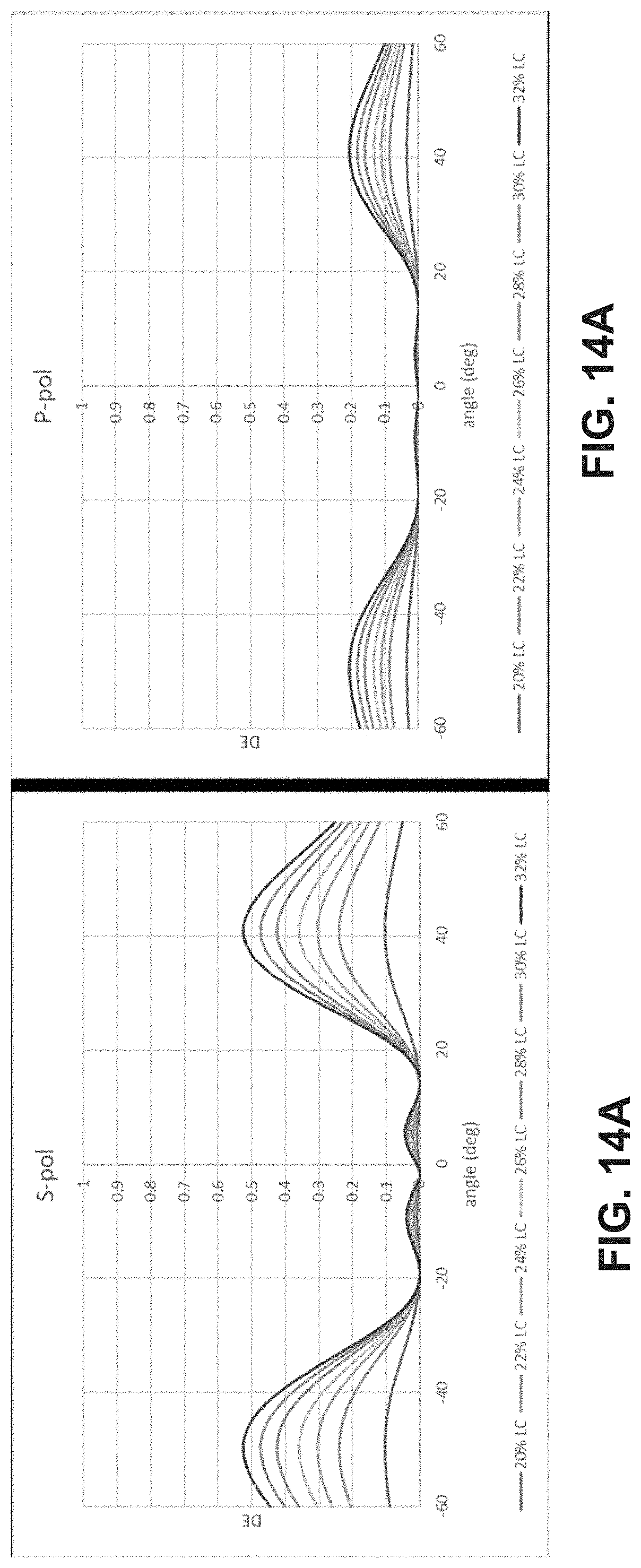
D00013
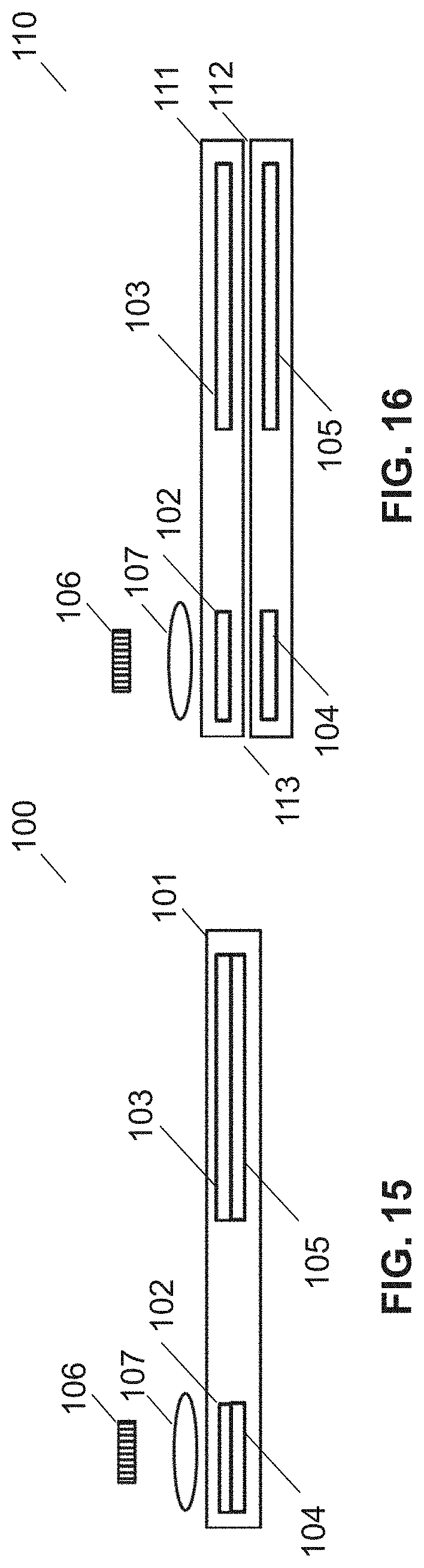
D00014

D00015
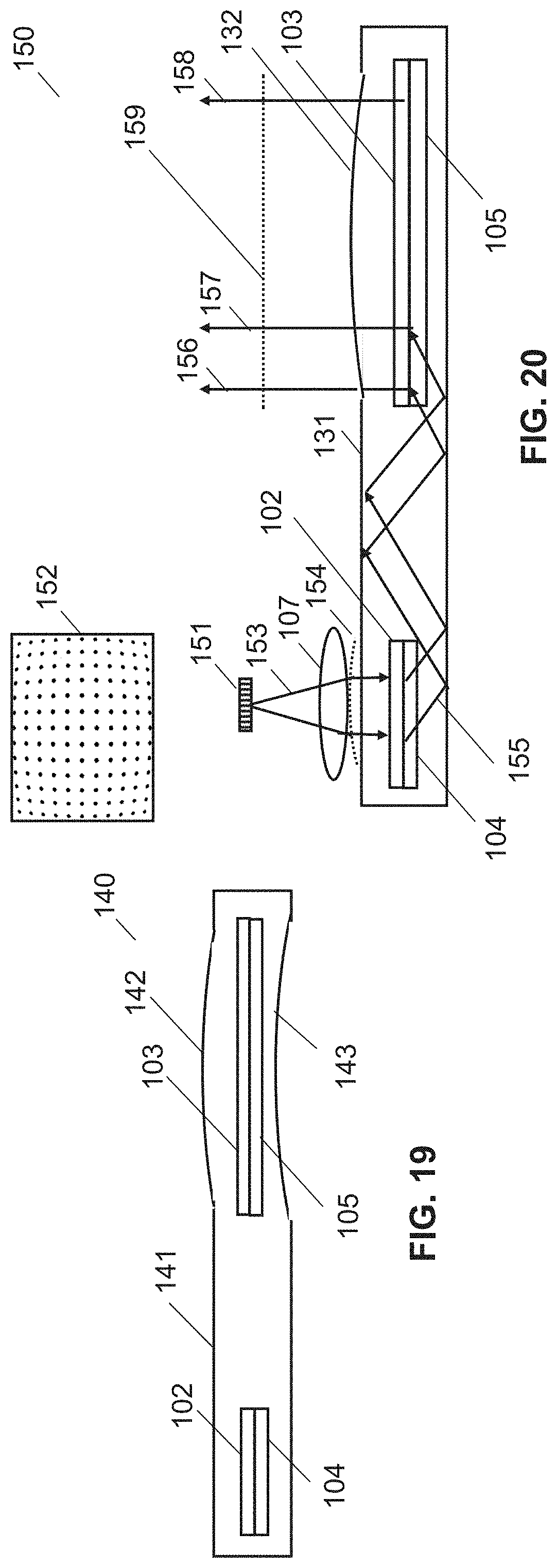
D00016
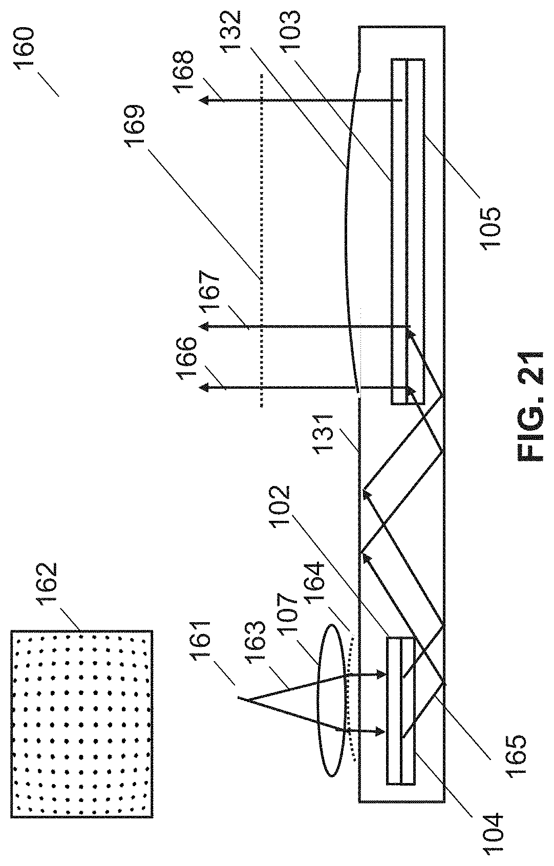
D00017

D00018

D00019
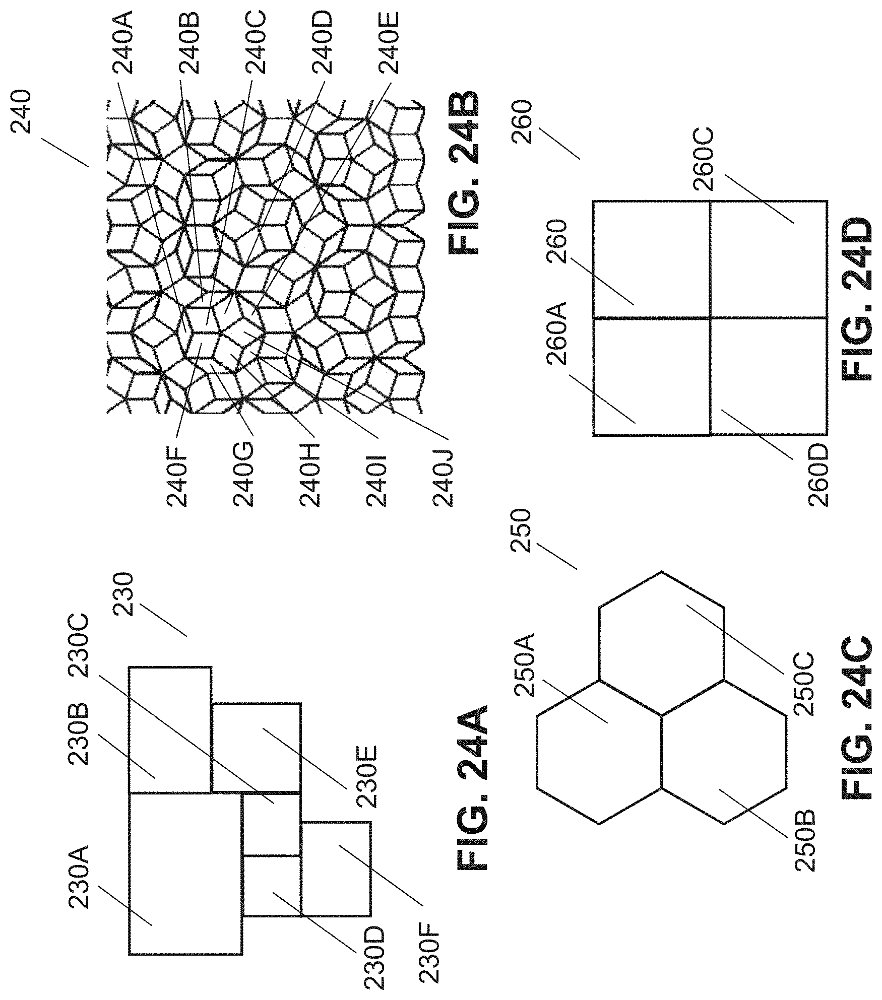
D00020

D00021
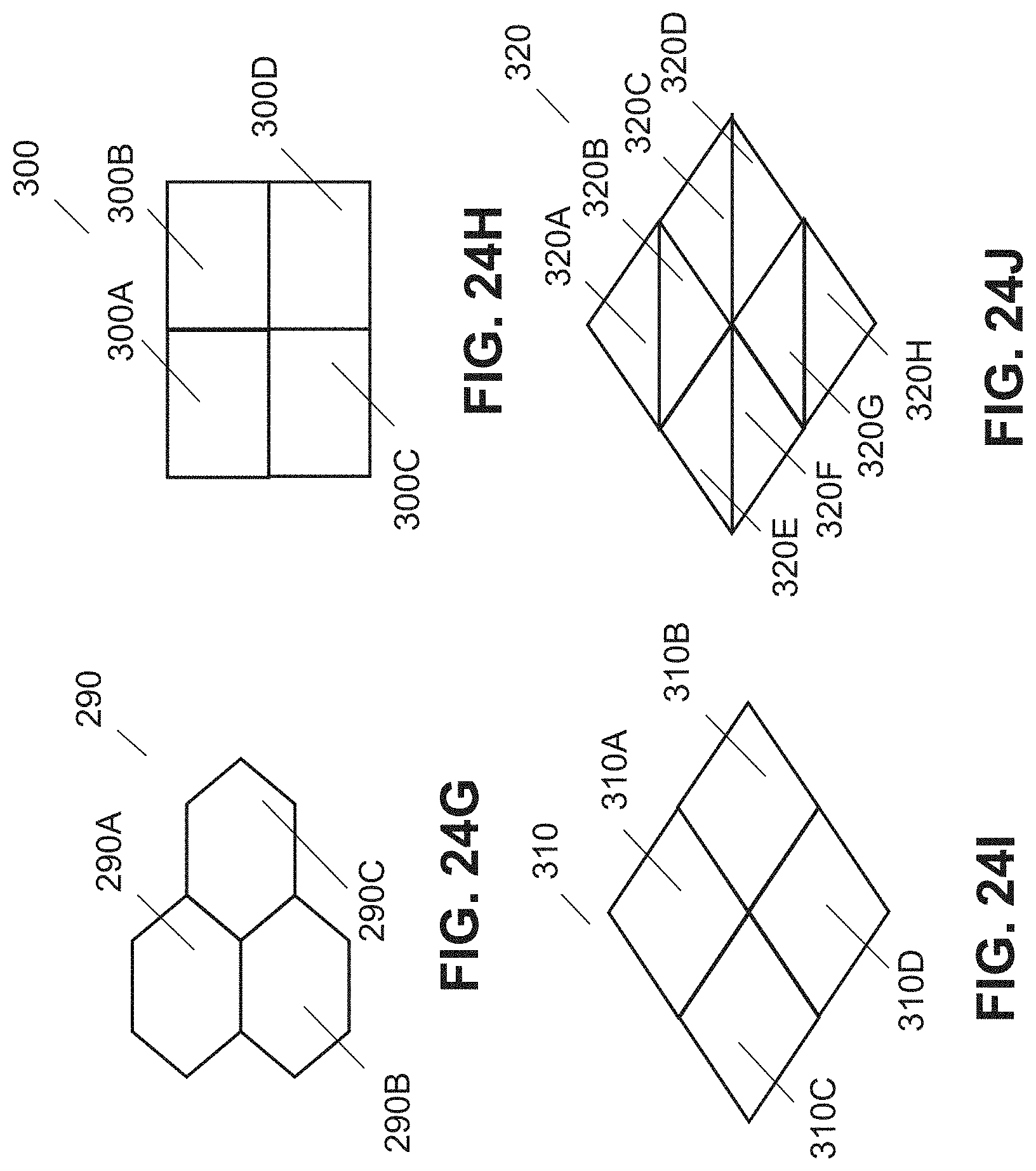
D00022
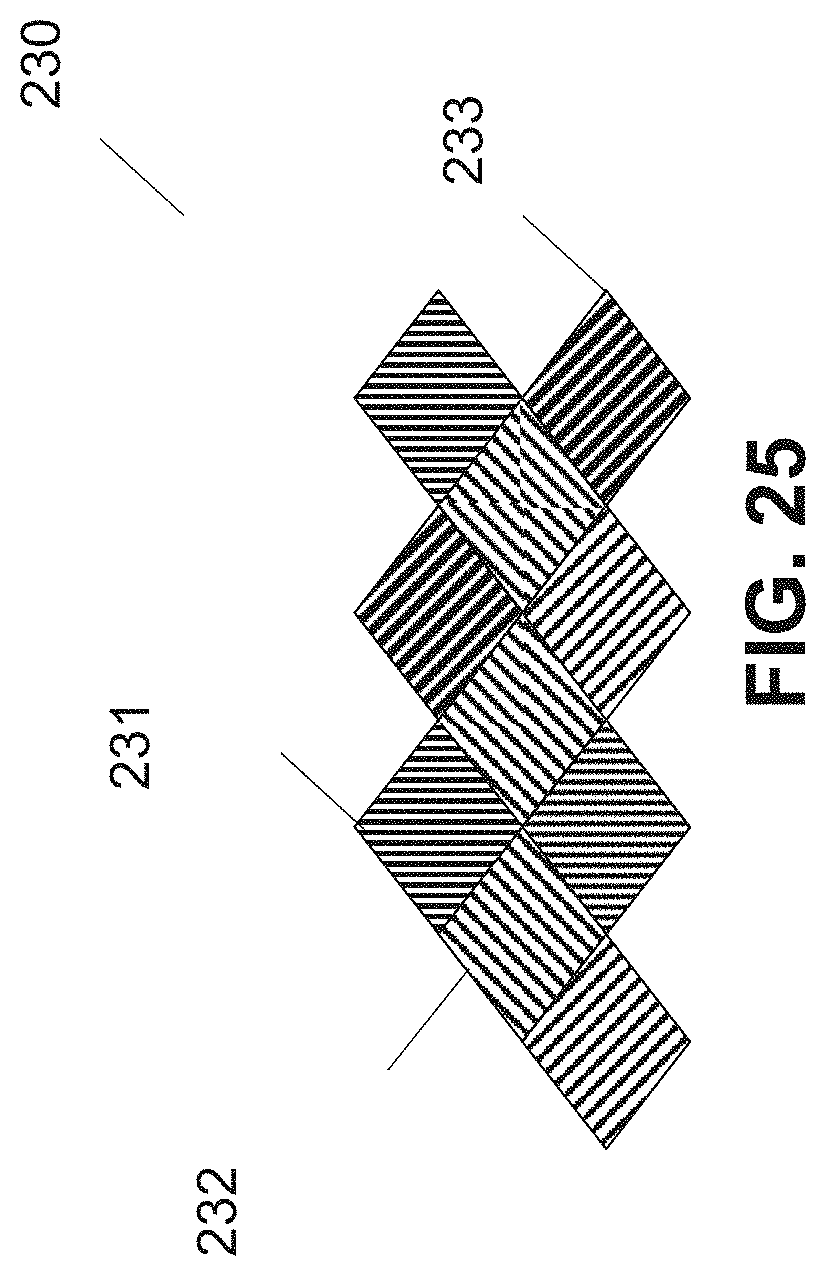
XML
uspto.report is an independent third-party trademark research tool that is not affiliated, endorsed, or sponsored by the United States Patent and Trademark Office (USPTO) or any other governmental organization. The information provided by uspto.report is based on publicly available data at the time of writing and is intended for informational purposes only.
While we strive to provide accurate and up-to-date information, we do not guarantee the accuracy, completeness, reliability, or suitability of the information displayed on this site. The use of this site is at your own risk. Any reliance you place on such information is therefore strictly at your own risk.
All official trademark data, including owner information, should be verified by visiting the official USPTO website at www.uspto.gov. This site is not intended to replace professional legal advice and should not be used as a substitute for consulting with a legal professional who is knowledgeable about trademark law.