Method For Preparing Ohmic Contact Electrode Of Gallium Nitride-based Device
TAN; Yongliang ; et al.
U.S. patent application number 16/968977 was filed with the patent office on 2021-02-25 for method for preparing ohmic contact electrode of gallium nitride-based device. The applicant listed for this patent is THE 13TH RESEARCH INSTITUTE OF CHINA ELECTRONICS TECHNOLOGY GROUP CORPORATION. Invention is credited to Yuxing CUI, Xingchang FU, Xingzhong FU, Zexian HU, Xiangwu LiU, Yongliang TAN, Lijiang ZHANG.
| Application Number | 20210057221 16/968977 |
| Document ID | / |
| Family ID | 1000005236133 |
| Filed Date | 2021-02-25 |


| United States Patent Application | 20210057221 |
| Kind Code | A1 |
| TAN; Yongliang ; et al. | February 25, 2021 |
METHOD FOR PREPARING OHMIC CONTACT ELECTRODE OF GALLIUM NITRIDE-BASED DEVICE
Abstract
A method for preparing an ohmic contact electrode of a GaN-based device. Said method comprises the following steps: growing a first dielectric layer (203) on an upper surface of a device (51); implanting silicon ions and/or indium ions in a region of the first dielectric layer (203) corresponding to an ohmic contact electrode region, and in the ohmic contact electrode region of the device (S2); growing a second dielectric layer (206) on an upper surface of the first dielectric layer (203) (S3); activating the silicon ions and/or the indium ions by means of a high temperature annealing process, so as to form an N-type heavy doping (S4); respectively removing portions, corresponding to the ohmic contact electrode region, of the first dielectric layer (203) and the second dielectric layer (206) (S5); growing a metal layer (208) on the upper surface of the ohmic contact electrode region of the device, so as to form an ohmic contact electrode (S6). The ohmic contact electrode prepared by the method can ensure that the metal layer (208) has flat surfaces, smooth and regular edges, and said electrode has stable device breakdown voltage, and is reliable and has a long service life.
| Inventors: | TAN; Yongliang; (Shijiazhuang, CN) ; FU; Xingzhong; (Shijiazhuang, CN) ; HU; Zexian; (Shijiazhuang, CN) ; LiU; Xiangwu; (Shijiazhuang, CN) ; ZHANG; Lijiang; (Shijiazhuang, CN) ; CUI; Yuxing; (Shijiazhuang, CN) ; FU; Xingchang; (Shijiazhuang, CN) | ||||||||||
| Applicant: |
|
||||||||||
|---|---|---|---|---|---|---|---|---|---|---|---|
| Family ID: | 1000005236133 | ||||||||||
| Appl. No.: | 16/968977 | ||||||||||
| Filed: | February 27, 2019 | ||||||||||
| PCT Filed: | February 27, 2019 | ||||||||||
| PCT NO: | PCT/CN2019/076323 | ||||||||||
| 371 Date: | August 11, 2020 |
| Current U.S. Class: | 1/1 |
| Current CPC Class: | H01L 21/31155 20130101; H01L 29/452 20130101; H01L 21/2258 20130101; H01L 21/31116 20130101; H01L 21/28575 20130101 |
| International Class: | H01L 21/225 20060101 H01L021/225; H01L 21/3115 20060101 H01L021/3115; H01L 21/285 20060101 H01L021/285 |
Foreign Application Data
| Date | Code | Application Number |
|---|---|---|
| Feb 28, 2018 | CN | 201810166841.8 |
Claims
1. A method for preparing an ohmic contact electrode of a gallium nitride (GaN)-based device, comprising following steps: step S1: growing a first dielectric layer on an upper surface of the device; step S2: implanting silicon ions and/or indium ions into a region of the first dielectric layer corresponding to an ohmic contact electrode region of the device and into the ohmic contact electrode region; step S3: growing a second dielectric layer on an upper surface of the first dielectric layer; step S4: activating the silicon ions and/or the indium ions using a high temperature annealing process, so as to form an N-type highly doped region; step S5: respectively removing portions, corresponding to the ohmic contact electrode region, of the first dielectric layer and the second dielectric layer; and step S6: growing a metal layer on an upper surface of the ohmic contact electrode region of the device, so as to form the ohmic contact electrode.
2. The method for preparing an ohmic contact electrode of a GaN-based device according to claim 1, wherein the step S2 comprises: step S21: applying a first photoresist layer to an upper surface of a portion of the first dielectric layer corresponding to a first region of the device, wherein the first region is a region other than the ohmic contact electrode region of the device; step S22: implanting the silicon ions and/or indium ions using ion implantation; and step S23: removing the first photoresist layer.
3. The method for preparing an ohmic contact electrode of a GaN-based device according to claim 1, wherein the S3 and the S4 comprising the following steps: step S31: applying a second photoresist layer to an upper surface of a portion of the second dielectric layer corresponding to the first region; step S32: removing portions of the first dielectric layer and the second dielectric layer corresponding to the ohmic contact electrode region respectively using a dry etching process; step 33: evaporation deposition of the metal layer on an upper surface of the device using an electron beam evaporation process; and step 34: removing the second photoresist layer.
4. The method for preparing an ohmic contact electrode of a GaN-based device according to claim 1, wherein the first dielectric layer is an SiN layer or an SiO.sub.2 layer, and the first dielectric layer has a thickness of 10 to 50 nanometers.
5. The method for preparing an ohmic contact electrode of a GaN-based device according to claim 1, wherein the second dielectric layer is an SiN layer or an AIN layer, and the second dielectric layer has a thickness of 10 to 200 nanometers.
6. The method for preparing an ohmic contact electrode of a GaN-based device according to claim 1, wherein the silicon ions have an implantation energy of 30 to 200 keV and an implantation dose of 10.sup.14cm.sup.-2 to 10.sup.16cm.sup.-2; and wherein the indium ions have an implantation energy of 30 to 200 keV and an implantation dose of 10.sup.13cm.sup.-2 to 10.sup.16cm.sup.-2.
7. The method for preparing an ohmic contact electrode of a GaN-based device according to claim 1, wherein the metal layer comprises a Ti/Au layer, a Ti/Pt/Au layer, a Ti/AI layer or a Ti/Al/Ni/Au layer.
8. The method for preparing an ohmic contact electrode of a GaN-based device according to claim 1, wherein the silicon ions and/or the indium ions have an implantation depth of 80 to 120 nanometers.
9. The method for preparing an ohmic contact electrode of a GaN-based device according to claim 1, wherein a process condition of the high temperature annealing process comprises: an annealing temperature of 850 to 1400.degree. C. and an annealing duration of 10 to 60 minutes.
10. The method for preparing an ohmic contact electrode of a GaN-based device according to claim 2, wherein a process condition of the high temperature annealing process comprises: an annealing temperature of 850 to 1400.degree. C. and an annealing duration of 10 to 60 minutes.
11. The method for preparing an ohmic contact electrode of a GaN-based device according to claim 3, wherein a process condition of the high temperature annealing process comprises: an annealing temperature of 850 to 1400.degree. C. and an annealing duration of 10 to 60 minutes.
12. The method for preparing an ohmic contact electrode of a GaN-based device according to claim 4, wherein a process condition of the high temperature annealing process comprises: an annealing temperature of 850 to 1400.degree. C. and an annealing duration of 10 to 60 minutes.
13. The method for preparing an ohmic contact electrode of a GaN-based device according to claim 5, wherein a process condition of the high temperature annealing process comprises: an annealing temperature of 850 to 1400.degree. C. and an annealing duration of 10 to 60 minutes.
14. The method for preparing an ohmic contact electrode of a GaN-based device according to claim 6, wherein a process condition of the high temperature annealing process comprises: an annealing temperature of 850 to 1400.degree. C. and an annealing duration of 10 to 60 minutes.
15. The method for preparing an ohmic contact electrode of a GaN-based device according to claim 7, wherein a process condition of the high temperature annealing process comprises: an annealing temperature of 850 to 1400.degree. C. and an annealing duration of 10 to 60 minutes.
16. The method for preparing an ohmic contact electrode of a GaN-based device according to claim 8, wherein a process condition of the high temperature annealing process comprises: an annealing temperature of 850 to 1400.degree. C. and an annealing duration of 10 to 60 minutes.
Description
[0001] The present application is filed based upon and claims priority to Chinese Patent Application No. 201810166841.8, filed on Feb. 28, 2018 and entitled "METHOD FOR PREPARING OHMIC CONTACT ELECTRODE OF GALLIUM NITRIDE-BASED DEVICE", the contents of which are hereby incorporated by reference in its entirety.
TECHNICAL FIELD
[0002] The disclosure relates to the field of semiconductor technology, and particularly to a method for preparing an ohmic contact electrode of a gallium nitride (GaN)-based device.
BACKGROUND
[0003] As a wide band gap semiconductor, GaN has some advantages such as wide band gap, high density two-dimensional electron gas when combined with AlGaN, high breakdown field strength and high saturated electron drift velocity, and it has great potential in the field of manufacturing of high temperature microwave power devices and high-speed power electronic devices. In a GaN-based device, a state-of-the-art ohmic contact electrode can not only improve the performance of the device but also prolong the working life of the device. A conventional method manufactures an ohmic contact electrode by performing a fast thermal annealing process on a metal layer in a temperature higher than 800.degree. C. But the ohmic contact electrode formed by the conventional method is low in quality, it has disadvantages such as rough metal surface topography and uneven metal edges, which may cause problems such as a high possibility of an electric breakdown in the devices and a decrease in the reliability and the life expectancy of the devices.
SUMMARY
Technical Problem
[0004] In view of the above, the embodiments of the disclosure provide a method for preparing an ohmic contact electrode of a GaN-based device to solve a problem that ohmic contact electrodes produced by current technologies are low in quality.
Technical Solutions
[0005] The embodiments of the disclosure provide a method for preparing an ohmic contact electrode of a GaN-based device and the method includes following steps:
[0006] step S1: a first dielectric layer is grown on an upper surface of the device;
[0007] step S2: silicon ions and/or indium ions are implanted into a region of the first dielectric layer corresponding to an ohmic contact electrode region of the device and into the ohmic contact electrode region;
[0008] step S3: a second dielectric layer is grown on an upper surface of the first dielectric layer;
[0009] step S4: the silicon ions and/or the indium ions are activated using a high temperature annealing process, so as to form an N-type highly doped region;
[0010] step S5: portions, corresponding to the ohmic contact electrode region, of the first dielectric layer and the second dielectric layer are respectively removed; and
[0011] step S6: a metal layer is formed on an upper surface of the ohmic contact electrode region of the device, so as to form the ohmic contact electrode.
[0012] According to an embodiment of the disclosure, the step S2 may specifically include following steps:
[0013] step S21: a first photoresist layer is applied to an upper surface of a portion of the first dielectric layer corresponding to a first region of the device, and the first region is a region other than the ohmic contact electrode region of the device;
[0014] step S22: the silicon ions and/or indium ions are implanted using ion implantation; and
[0015] step S23: the first photoresist layer is removed.
[0016] According to an embodiment of the disclosure, S3 and S4 may specifically include following steps:
[0017] step S31: a second photoresist layer is applied to an upper surface of a portion of the second dielectric layer corresponding to the first region;
[0018] step S32: portions of the first dielectric layer and the second dielectric layer corresponding to the ohmic contact electrode region respectively are removed using a dry etching process;
[0019] step S33: evaporation deposition of the metal layer on an upper surface of the device is performed using an electron beam evaporation process; and
[0020] step 34: the second photoresist layer is removed.
[0021] According to an embodiment of the disclosure, the first dielectric layer may be an SiN layer or an SiO.sub.2 layer, and the first dielectric layer may have a thickness of 10 to 50 nanometers.
[0022] According to an embodiment of the disclosure, the second dielectric layer may be an SiN layer or an MN layer, and the second dielectric layer may have a thickness of 10 to 200 nanometers.
[0023] According to an embodiment of the disclosure, the silicon ions may have an implantation energy of 30 to 200 keV and an implantation dose of 10.sup.14cm.sup.-2 to 10.sup.16cm.sup.2 and the indium ions may have an implantation energy of 30 to 200 keV and an implantation dose of 10.sup.13cm.sup.-2 to 10.sup.16cm.sup.-2;
[0024] According to an embodiment of the disclosure, the metal layer may include a Ti/Au layer, a Ti/Pt/Au layer, a Ti/Al layer or a Ti/Al/Ni/Au layer.
[0025] According to an embodiment of the disclosure, the silicon ions and/or the indium ions may have an implantation depth of 80 to 120 nanometers.
[0026] According to an embodiment of the disclosure, a process condition of the high temperature annealing process may include: an annealing temperature of 850 to 1400.degree. C. and an annealing duration of 10 to 60 minutes
Beneficial Effects
[0027] In the embodiments of the disclosure, a first dielectric layer is grown on an upper surface of a device as an ion implantation scattering layer, silicon ions and/or indium ions are implanted into an ohmic contact electrode region of the device and into a region of the first dielectric layer corresponding to the ohmic contact electrode region, a second dielectric layer is grown on an upper surface of the first dielectric layer as a protective layer, the silicon ions and/or the indium ions are activated using a high temperature annealing process, so as to form an N-type highly doped region, finally portions, corresponding to the ohmic contact electrode region, of the first dielectric layer and the second dielectric layer are removed so that the ohmic contact electrode region is exposed, and a metal layer is formed on an upper surface of the ohmic contact electrode region of the device, so as to form the ohmic contact electrode. Because the metal layer does not need to undergo the high temperature annealing process, the ohmic contact electrodes with good quality can be manufactured, which can guarantee that the metal layer has an smooth surface and edges, and the device has a steady breakdown voltage, good reliability and long life expectancy.
BRIEF DESCRIPTION OF THE DRAWINGS
[0028] FIG. 1 is a schematic diagram illustrating an implementation flow of a method for preparing an ohmic contact electrode of a GaN-based device according to an embodiment of the disclosure;
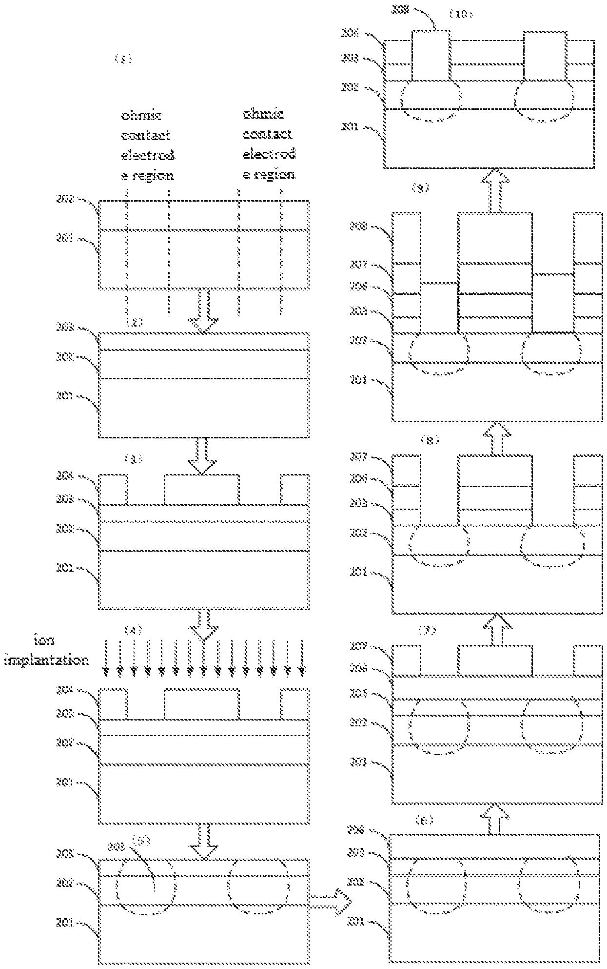
[0029] FIG. 2 is a schematic diagram illustrating structures obtained during an implementation flow of the method for preparing an ohmic contact electrode of a GaN-based device according to an embodiment of the disclosure.
DETAILED DESCRIPTION
[0030] The technical solution in the disclosure will be described as follows in combination with the embodiments of the disclosure.
[0031] Referring to FIG. 1, the method for preparing an ohmic contact electrode of a GaN-based device includes the following steps S1 to S6.
[0032] In step S1, a first dielectric layer is grown on an upper surface of the device.
[0033] In an embodiment of the disclosure, the first dielectric layer is an SiN layer or an SiO2 layer, has a thickness of 10 to 50 nanometers and can be used as an ion implantation scattering layer in subsequent processes.
[0034] Referring to FIG. 2 (1), the GaN-based device in the embodiment of the disclosure includes a GaN substrate 201 and an AlGaN layer 202, and the GaN-based device includes ohmic contact electrode regions and a first region. The first region is a region other than the ohmic contact electrode regions of the device, and the ohmic contact electrodes are prepared in the ohmic contact electrode regions of the GaN-based device. Referring to FIG. 2 (2), a first dielectric layer 203 is deposited on an upper surface of the AlGaN layer 202 as an ion implantation scattering layer using chemical vapor deposition.
[0035] In step S2, silicon ions and/or indium ions are implanted into a region of the first dielectric layer corresponding to an ohmic contact electrode region of the device and into the ohmic contact electrode region.
[0036] In the embodiment of the disclosure, the silicon ions have an implantation energy of 30 to 200 keV and an implantation dose of 10.sup.14cm.sup.-2 to 10.sup.16cm.sup.-2 and the indium ions have an implantation energy of 30 to 200 keV and an implantation dose of 10.sup.13cm.sup.-2 to 10.sup.16cm.sup.-2.
[0037] According to an embodiment of the disclosure, a specific implementation of the step S2 is: a first photoresist layer is applied to an upper surface of a portion of the first dielectric layer corresponding to a first region of the device, and the first region is a region other than the ohmic contact electrode regions of the device; the silicon ions and/or indium ions are implanted using ion implantation; and the first photoresist layer is removed.
[0038] Referring to FIG. 2 (3) to FIG. 2(5), the upper surface of the portion of the first dielectric layer corresponding to the first region is covered with the first photoresist layer 204 by using processes of photoresist application, exposure, development and hardening so that portions of the first dielectric layer corresponding to the ohmic contact electrode regions are exposed. The first photoresist layer 204 has a thickness of 2 to 5 micrometers. Then silicon ions and/or indium ions are implanted using ion implantation and the ions are merely implanted into the exposed portions of first dielectric layer 204 corresponding to the ohmic contact electrode regions and into the ohmic contact electrode regions of the device, i.e., the dotted regions designated 205 in FIG. 2 (5); and the ions will not be implanted into other portions because the other portions are protected by the first photoresist layer 204; finally the first photoresist layer 204 is removed.
[0039] In step S3, a second dielectric layer is grown on an upper surface of the first dielectric layer.
[0040] In the embodiment of the disclosure, referring to FIG. 2 (6); the second dielectric layer 206 includes an SiN layer or an MN layer, and the second dielectric layer 206 has a thickness of 10 to 200 nanometers. The second dielectric layer is used as a protective layer in the subsequent high temperature annealing process.
[0041] In step S4, the silicon ions and/or the indium ions are activated using a high temperature annealing process, so as to form an N-type highly doped region.
[0042] In the embodiment of the disclosure, the annealing temperature is 850 to 1400.degree. C. and the annealing lasts 10 to 60 minutes. The implanted silicon ions and/or indiums ions activated by the high temperature annealing process enables the formation of N-type highly doped regions.
[0043] In step S5, portions, corresponding to the ohmic contact electrode region, of the first dielectric layer and the second dielectric layer are respectively removed.
[0044] In step S6, a metal layer is grown on an upper surface of the ohmic contact electrode region of the device, so as to form the ohmic contact electrode.
[0045] In the embodiment of the disclosure, the metal layer is a Ti/Au layer, a Ti/Pt/Au layer, a Ti/Al layer or a Ti/Al/Ni/Au layer.
[0046] Referring to FIG. 2 (7) to FIG. 2 (10), a specific implementation of the step S5 and the step S6 is: the second photoresist layer 207 is applied to the upper surface of the portion of the second dielectric layer 206 corresponding to the first region; the portions of the first dielectric layer 203 and the second dielectric layer 206 corresponding to the ohmic contact electrode regions are removed respectively using the dry etching process; the evaporation deposition of the metal layer 208 on an upper surface of the device is performed using the electron beam evaporation process; and the second photoresist layer 207 is removed.
[0047] In the embodiment of the disclosure, the upper surface of the portion of the second dielectric layer 206 corresponding to the first region is covered with the second photoresist layer 207 by using processes of photoresist application, exposure, development and hardening to expose the portions of the second dielectric layer 206 corresponding to the ohmic contact electrode regions. The second photoresist layer 207 has a thickness of 1 to 2 micrometers. The portions of the first dielectric layer 203 and the second dielectric layer 206 corresponding to the ohmic contact electrode regions are removed using the dry etching process to expose the ohmic contact regions of the device. The metal layer 208 is subjected to the evaporation deposition using the electron beam evaporation process and finally the second photoresist layer 207 is removed. The metal layer 208 contacts the N-type highly doped AlGaN layer 202 and forms an ohmic contact.
[0048] In the embodiments of the disclosure, the first dielectric layer 203 is grown on the upper surface of the device as the ion implantation scattering layer, silicon ions and/or indium ions are implanted into the ohmic contact electrode region of the device and into the region of the first dielectric layer 203 corresponding to the ohmic contact electrode region, the second dielectric layer 206 is grown on the upper surface of the first dielectric layer as the protective layer, the silicon ions and/or the indium ions are activated using the high temperature annealing process, so as to form the N-type highly doped region, finally portions, corresponding to the ohmic contact electrode region, of the first dielectric layer 203 and the second dielectric layer 206 are removed so that the ohmic contact electrode region is exposed, and the metal layer 208 is grown on the upper surface of the ohmic contact electrode region of the device, so as to form the ohmic contact electrode. Because the metal layer does not need to undergo the high temperature annealing process, the ohmic contact electrodes of with good quality can be manufactured, which can guarantee that the metal layer has an even surface and smooth and clean edges, and the device has a steady breakdown voltage, good reliability and long life expectancy.
[0049] It can be understood that the numbers of all the steps in the above embodiments of the disclosure do not necessarily stand for their implementation order, and the implementation order of each process should be determined by its function and inner logic, thus the sequence indicated by the numbers of all the steps is not intended to limit an implementation process of the embodiments of the disclosure.
[0050] The above-mentioned embodiments of the disclosure are merely used to describe rather than limit the technical solutions of the disclosure. Although the disclosure is described in detail according to the above-mentioned embodiments of the disclosure, those skilled in the art should understand that the technical solutions recited in respective above-mentioned embodiments of the disclosure can be modified or parts of technical features in the technical solutions can be substituted by technically equivalent elements. The modifications or substitutions without departing from the spirit and the scope of the technical solutions of the embodiments of the disclosure all fall within the scope of protection of the disclosure.
* * * * *
D00000
D00001
D00002
XML
uspto.report is an independent third-party trademark research tool that is not affiliated, endorsed, or sponsored by the United States Patent and Trademark Office (USPTO) or any other governmental organization. The information provided by uspto.report is based on publicly available data at the time of writing and is intended for informational purposes only.
While we strive to provide accurate and up-to-date information, we do not guarantee the accuracy, completeness, reliability, or suitability of the information displayed on this site. The use of this site is at your own risk. Any reliance you place on such information is therefore strictly at your own risk.
All official trademark data, including owner information, should be verified by visiting the official USPTO website at www.uspto.gov. This site is not intended to replace professional legal advice and should not be used as a substitute for consulting with a legal professional who is knowledgeable about trademark law.