Semiconductor Power Device And Method For Manufacture
LIU; Mingjiao
U.S. patent application number 16/667631 was filed with the patent office on 2021-02-18 for semiconductor power device and method for manufacture. This patent application is currently assigned to SEMICONDUCTOR COMPONENTS INDUSTRIES, LLC. The applicant listed for this patent is SEMICONDUCTOR COMPONENTS INDUSTRIES, LLC. Invention is credited to Mingjiao LIU.
| Application Number | 20210050458 16/667631 |
| Document ID | / |
| Family ID | 1000004525078 |
| Filed Date | 2021-02-18 |


View All Diagrams
| United States Patent Application | 20210050458 |
| Kind Code | A1 |
| LIU; Mingjiao | February 18, 2021 |
SEMICONDUCTOR POWER DEVICE AND METHOD FOR MANUFACTURE
Abstract
A device includes a first doped semiconductor region and a second oppositely doped semiconductor region that are separated by an undoped or lightly-doped semiconductor drift region. The device further includes a first electrode structure making an ohmic contact with the first doped semiconductor region, and a second electrode structure making a universal contact with the second doped semiconductor region. The universal contact of the second electrode structure allows flow of both electrons and holes into, and out of, the device.
| Inventors: | LIU; Mingjiao; (Gilbert, AZ) | ||||||||||
| Applicant: |
|
||||||||||
|---|---|---|---|---|---|---|---|---|---|---|---|
| Assignee: | SEMICONDUCTOR COMPONENTS
INDUSTRIES, LLC Phoenix AZ |
||||||||||
| Family ID: | 1000004525078 | ||||||||||
| Appl. No.: | 16/667631 | ||||||||||
| Filed: | October 29, 2019 |
Related U.S. Patent Documents
| Application Number | Filing Date | Patent Number | ||
|---|---|---|---|---|
| 62887759 | Aug 16, 2019 | |||
| Current U.S. Class: | 1/1 |
| Current CPC Class: | H01L 29/868 20130101; H01L 29/47 20130101; H01L 29/6609 20130101 |
| International Class: | H01L 29/868 20060101 H01L029/868; H01L 29/47 20060101 H01L029/47; H01L 29/66 20060101 H01L029/66 |
Claims
1. A device comprising: a first doped semiconductor region and a second oppositely doped semiconductor region that are separated by an undoped or lightly-doped semiconductor drift region; a first electrode structure making an ohmic contact with the first doped semiconductor region; a second electrode structure making a universal contact with the second doped semiconductor region, the universal contact allowing flow of both electrons and holes.
2. The device of claim 1, wherein the second electrode structure includes at least one P+ doped semiconductor region and at least one N+ doped semiconductor region in contact with the second doped semiconductor region.
3. The device of claim 2, wherein the second electrode structure includes a metal or metal alloy layer, and at least one P+ doped semiconductor region and the at least one N+ doped semiconductor region are disposed between the metal or metal alloy layer and the second doped semiconductor region.
4. The device of claim 3, wherein the second electrode structure further includes an oxide layer disposed between the at least one P+ doped semiconductor region and the metal or metal alloy layer.
5. The device of claim 3, wherein the second electrode structure includes a plurality of P+ doped semiconductor regions alternating with a plurality of N+ doped semiconductor regions disposed between the metal or metal alloy layer and the second doped semiconductor region.
6. The device of claim 1, wherein the at least one P+ doped semiconductor region has a first area of contact with the second doped semiconductor region, and the at least one N+ doped semiconductor region has a second area of contact with the second doped semiconductor region, a ratio of the first area and the second area forming a p-to-n areal ratio of the universal contact.
7. The device of claim 6, wherein the p-to-n areal ratio determines a reverse current recovery time of the device.
8. The device of claim 6, wherein the p-to-n areal ratio determines a forward current of the device.
9. The device of claim 6, wherein the p-to-n areal ratio is between 0.2:1 and 5:1.
10. The device of claim 1, wherein the first doped semiconductor region is a p doped semiconductor region, the second doped semiconductor region is an N-type semiconductor substrate region having a resistivity in a range of 0.001 to 50 .OMEGA.-cm, and the undoped or lightly-doped semiconductor drift region is an n-type epitaxial semiconductor region having a resistivity in a range of 20 to 200 .OMEGA.-cm.
11. The device of claim 9, wherein first electrode structure includes a P+ layer formed on a top surface of the n-type epitaxial layer and a metal layer deposited on the P+ layer.
12. A device comprising: a first doped semiconductor region and a second oppositely doped semiconductor region that are separated by an undoped or lightly-doped semiconductor drift region; a first electrode structure making an ohmic contact with the first doped semiconductor region; a second electrode structure including an alternating array of P+ doped semiconductor regions and N+ doped semiconductor regions in contact with second doped semiconductor region, the second electrode structure including an oxide layer disposed between a metal layer and the P+ doped semiconductor regions and the N+ doped semiconductor regions of the alternating array.
13. The device of claim 12, wherein the oxide layer covers the P+ doped semiconductor regions and extends partially over the N+ doped semiconductor regions of the alternating array.
14. A method comprising: growing an n-type epitaxial layer on a N-type semiconductor substrate; forming an anode structure on a top surface of the n-type epitaxial layer; back grinding the N-type semiconductor substrate to reduce its thickness; and forming a cathode structure including: forming a universal contact structure on a back surface of the back-ground semiconductor substrate; and depositing a back metal on a back surface of universal contact structure.
15. The method of claim 14, wherein forming the universal contact structure includes: implanting a n-dopant into the back surface of the back-ground semiconductor substrate; implanting a p-dopant into the back surface of the back-ground semiconductor substrate; photolithographic patterning to delineate P+ regions and the N+ regions of the universal contact structure; implanting an n-dopant to form the N+ regions of the universal contact structure; and laser annealing to activate the implanted p-dopant and n-dopant to form the P+ regions and the N+ regions of the universal contact structure.
16. The method of claim 15, wherein forming the universal contact structure further includes: patterning and depositing an oxide layer over the P+ regions and partially over the N+ regions of the universal contact structure.
17. The method of claim 16 further comprising: depositing the back metal over the oxide layer.
18. The method of claim 17, wherein the N-type semiconductor substrate has a resistivity in a range of 0.01 to 10 .OMEGA.-cm, and the n-type epitaxial layer has a resistivity in a range of 20 to 200 .OMEGA.-cm.
19. The method of claim 18, wherein forming the anode structure includes forming a P+ layer on a top surface of the n-type epitaxial layer and depositing a metal layer on the P+ layer.
20. The method of claim 19, wherein forming the P+ layer includes thermal diffusion, and/or implantation, of p dopant species into the top surface of the n-type epitaxial layer.
Description
TECHNICAL FIELD
[0001] The present disclosure relates to devices for power electronics such as a free-wheeling or flyback diode that can be connected across an inductor and used to eliminate flyback, which is the sudden voltage spike seen across an inductive load when its supply current is suddenly reduced or interrupted.
BACKGROUND
[0002] A free-wheeling or flyback diode (also called fast recovery diode (FRD) herein) is used to prevent damage to circuits that typically include a load that has an inductor and a switching potential. An inductor cannot change current immediately. Attempting to change the current rapidly such as when a switch opens after an inductor has built up energy, will cause the inductor to generate large electromotive forces (EMFs). A free wheeling diode placed anti-parallel to the inductor provides a short circuit path for a flow of inductor decay current and hence dissipation of the energy stored in the inductor.
[0003] In power electronic circuits for many switching applications (e.g., industrial and automotive inverter applications) semiconductor devices (e.g., a metal oxide semiconductor field effect transistor (MOSFET), an insulated-gate bipolar transistor (IGBT), etc.) are used as switches to apply power to inductive loads. In the power electronic circuits, a free-wheeling diode is placed anti parallel to the switch (e.g., IGBT) to provide a return path for inductor discharge currents. An FRD can contribute to significant power loss in a switching circuit (e.g., in the power inverter application of an IGBT). It is important that the FRD is designed for a stable operation without oscillation, and for low electromagnetic interference (EMI) in the switching circuit. A desirable FRD may have low loss, fast switching, and soft reverse current recovery characteristics. Attaining these FRD characteristics can involve a trade-off between diode parameters such as low forward voltage (VF), low reverse recovery charge (Qrr), and between high operating voltage and soft reverse current recovery.
SUMMARY
[0004] In a general aspect, a device includes a first doped semiconductor region and a second oppositely doped semiconductor region that are separated by an undoped or lightly-doped semiconductor drift region. The device further includes a first electrode structure making an ohmic contact with the first doped semiconductor region, and a second electrode structure making a universal contact with the second doped semiconductor region. The universal contact of the second electrode structure allows flow of both electrons and holes into, and out of, the device.
[0005] In an aspect, an alternating array of P+ doped semiconductor regions and N+ doped semiconductor regions in the second electrode structure make the universal contact with the second doped semiconductor region.
[0006] In a general aspect, a device includes a first doped semiconductor region and a second oppositely doped semiconductor region that are separated by an undoped or lightly-doped semiconductor drift region. The device further includes a first electrode structure making an ohmic contact with the first doped semiconductor region, and a second electrode structure including an alternating array of P+ doped semiconductor regions and N+ doped semiconductor regions in contact with second doped semiconductor region. The second electrode structure includes an oxide layer disposed between a metal layer and the P+ doped semiconductor regions and the N+ doped semiconductor regions of the alternating array.
[0007] In an aspect, the oxide layer covers the P+ doped semiconductor regions and extends partially over the N+ doped semiconductor regions of the alternating array, in the second electrode structure.
[0008] In a general aspect, a method includes growing an n-type epitaxial layer on a N-type semiconductor substrate, forming an anode structure on a top surface of the n-type epitaxial layer, back grinding the N-type semiconductor substrate to reduce its thickness, and forming a cathode structure on a back surface of the back-ground N-type semiconductor substrate. Forming the cathode structure includes forming a universal contact structure on the back surface of the back-ground semiconductor substrate and depositing a back metal on the back surface of universal contact structure.
BRIEF DESCRIPTION OF THE DRAWINGS
[0009] FIGS. 1A and 1B are diagrams that illustrate electrode structures of a p-i-n diode, consistent with the present disclosure.
[0010] FIG. 2 illustrates a reverse recovery current of the p-i-n diode of FIG. 1A, consistent with the present disclosure.
[0011] FIG. 3 illustrates a diode with an example cathode structure including a universal contact to a diode, consistent with the present disclosure.
[0012] FIG. 4 is an illustration of example method for fabricating a diode with soft recovery characteristics, consistent with the present disclosure.
[0013] FIGS. 5A through 5F schematically illustrate a cross-sectional view of portions of a semiconductor substrate as it is being processed at different stages or steps of the method of FIG. 4 to make a diode.
[0014] FIGS. 6A and 6B illustrate example dopant concentrations in a rectangular cross section of an example diode not having a universal contact in its cathode structure.
[0015] FIGS. 7A and 7B illustrate example dopant concentrations in a rectangular cross section of an example diode having a universal contact in its cathode structure.
[0016] FIG. 8 is a graph illustrating simulated reverse recovery currents and voltages for an example diode without a backside p-n junction, and an example diode having a backside p-n junction in its cathode structure.
[0017] FIG. 9A is a graph illustrating simulated reverse recovery currents for a set of diodes having different p-to-n areal ratios in the universal contacts of the diodes.
[0018] FIG. 9B is an exploded view of a portion of the graph of FIG. 9A.
[0019] FIG. 10 is a graph illustrating simulated forward currents (IF) as a function of forward voltage (VF) for a set of diodes having different p-to-n areal ratios in the universal contacts of the diodes.
[0020] FIG. 11 is a graph illustrating simulated reverse load currents (IR) as a function of load voltage (VR) for the same set of diodes as FIG. 10.
[0021] FIG. 12 is a graph illustrating simulated reverse recovery currents for a diode with no oxide layer included in its universal contact and a diode with an oxide layer covering the p-regions of its universal contact.
[0022] FIG. 13 is a graph illustrating simulated forward currents for the diodes of FIG. 12.
DETAILED DESCRIPTION
[0023] A p-i-n diode includes two oppositely doped semiconductor regions that are separated by an undoped or lightly-doped semiconductor drift region. Each of the two oppositely doped semiconductor regions is in electrical contact (ohmic contact) with a respective electrode (i.e., an anode or a cathode) of the device which allows flow of charge carriers (i.e., holes or electrons) into, and out of, the respective doped semiconductor region of the diode.
[0024] In accordance with the principles of the present disclosure, at least one of the electrodes is configured as a universal contact that allows flow of both holes and electrons) into, and out of, the respective doped semiconductor region of the diode.
[0025] The universal contact to a doped semiconductor region of the diode may have a structure that includes both P-doped semiconductor regions and N-doped semiconductor regions in contact with the respective doped semiconductor region of the diode. The P-doped semiconductor regions and N-doped semiconductor regions may be present in different areas of the universal contact. A p-to-n areal ratio can be used as a figure of merit to describe a ratio of an area of the universal contact occupied by P-doped semiconductor regions and an area of the universal contact occupied by N-doped semiconductor regions. The p-to-n areal ratio is selected in consideration of the reverse current recovery time of the device, and in consideration of the forward current of the device.
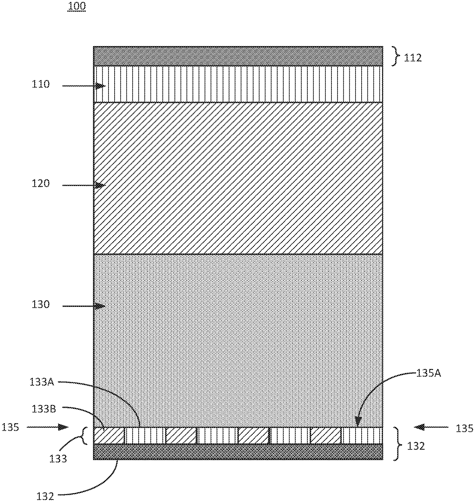
[0026] FIG. 1A illustrates an example structure of an example free wheeling diode (e.g., FRD 100), in accordance with the principles of the present disclosure. FRD 100 may have soft recovery characteristics for use in power switching circuits.
[0027] With reference to FIG. 1A, FRD 100 which may have a p-i-n diode-like structure that includes two oppositely doped semiconductor regions (110, 130) that are separated by a semiconductor drift region 120. Semiconductor region 110 may, for example, be a p-doped semiconductor region, and semiconductor region 130 may be an n-doped semiconductor region. Semiconductor drift region 120 may, for example, be a semiconductor region that is undoped or is lightly doped compared to the two oppositely doped semiconductor regions 110, 130. The two oppositely doped semiconductor regions 110, 130 may be heavily doped because they are used for making electrode structures (e.g., anode structure 112 and cathode structure 132, respectively) of FRD 100.
[0028] Anode structure 112 may, for example, be a metal or metal alloy layer that makes ohmic contact with semiconductor region 110 (e.g., a p-doped semiconductor region) allowing transport of holes into semiconductor region 110.
[0029] Further, in accordance with the principles of the present disclosure, a device electrode structure (e.g., cathode structure 132) may include a universal contact structure 133 interposed between a metal or metal alloy layer 134 and semiconductor region 130 (e.g., n-doped semiconductor region). Universal contact structure 133 may include a semiconductor region (e.g., semiconductor region 133A of opposite polarity to that of semiconductor region 130) forming a p-n junction 135A along at least a part of an interface 135 between universal contact structure 133 and semiconductor region 130. In example implementations, universal contact structure 133 may include at least one pair of semiconductor regions (133A, 133B) that alternate in a lateral direction (along interface 135 between universal contact structure 133 and semiconductor region 130). Semiconductor region 133A may for example, be a heavily P+ doped semiconductor region, while semiconductor region 133B may for example, be a heavily N+ doped semiconductor region. Semiconductor region 133A (a backside p doped region) forms a p-n junction 135A (a backside p-n junction) with a part of a lateral area or extent of semiconductor region 130 along interface 135.
[0030] In example implementations, the semiconductor regions (133A, 133B) of the universal contact structure 133 may occupy different areas along interface 135.
[0031] FIG. 1B (which is an exploded partial cross-sectional view of FRD 100 shown in FIG. 1A) shows, for example, semiconductor region 133A as being present along a length L1 of interface 135, while semiconductor regions 133B as being present along a different length L2 of interface 135. Thus, in the example shown in FIG. 1B, semiconductor region 133A and semiconductor region 133B of universal contact structure 133 are present (assuming a same depth of the semiconductor regions perpendicular to the plane of FIG. 1B) in an areal ratio of L1:L2 along interface 135. The areal ratio of semiconductor region 133A and semiconductor region 133B along interface 135 may be referred to hereinafter as the p-to-n areal ratio of the universal contact structure 133.
[0032] Universal contact structure 133 may make a contact with semiconductor region 130 that allows transport of both holes and electrons into semiconductor region 130. The holes may be transported into semiconductor region 130, for example, via P+ doped semiconductor regions 133A, and the electrons may be transported into semiconductor region 130, for example, via N+ doped semiconductor regions 133B.
[0033] When switching from a conducting to a blocking state, FRD 100 has stored charge (e.g., reverse recovery charge (Qrr)) in, for example, semiconductor drift region 120, that must first be discharged before FRD 100 blocks reverse current. This discharge takes a finite amount of time known as the reverse recovery time, or t.sub.rr. Cathode structure 132 by allowing transport of holes into FRD 100 via P+ doped semiconductor regions 133A (in addition to the transport of holes into semiconductor region 110 via the ohmic contact made by anode structure 112) would increase the reverse recovery time of FRD 100 over that of a conventional p-i-n diode structure (not shown) with conventional ohmic anode and cathode contacts (i.e., non-universal contacts) by increasing the tail of reverse recovery current.
[0034] The increased reverse recovery time t.sub.rr of FRD 100 can contribute to a soft recovery characteristic of FRD 100. FIG. 2 shows schematically a reverse recovery current 210 of FRD 100, which has a reverse recovery time t.sub.rr. FIG. 2 also shows schematically, for comparison, a reverse recovery current 220 of a conventional p-i-n diode, which has a comparable reverse recovery time t.sub.rr.
[0035] As shown in FIG. 2, reverse recovery current 210 of FRD 100 has a smooth profile gradually returning to a zero value and hence may be characterized as being a "soft" recovery. In contrast, reverse recovery current 220 of the conventional p-i-n diode has a noisy (i.e., snappy, not smooth) return to a zero value and hence may be characterized as being a "hard" recovery.
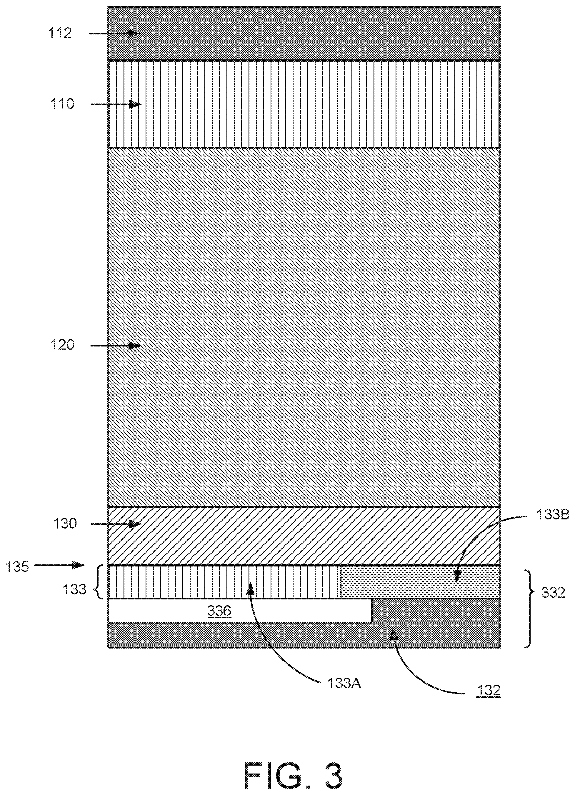
[0036] FIG. 3 illustrates FRD 100 with another example cathode structure for a universal contact to a diode, in accordance with the principles of the present disclosure. As shown in FIG. 3, FRD 100 can include a different cathode structure 332 other than cathode structure 132 shown in FIG. 1A.
[0037] Cathode structure 332 while generally similar to cathode structure 132 of FRD 100 (shown in FIG. 1A), further includes an oxide layer 336 interposed between universal contact structure 133 and metal layer 134. In example implementations, oxide layer 336 may overlay P+ semiconductor region 133A and may extend partially over N+ semiconductor region 133B. Oxide layer 336 overlaying P+ semiconductor region 133A may act as a barrier to the flow of holes, prevent leakage of holes out of FRD 100 through cathode 332, and further improves the characteristics of the diode.
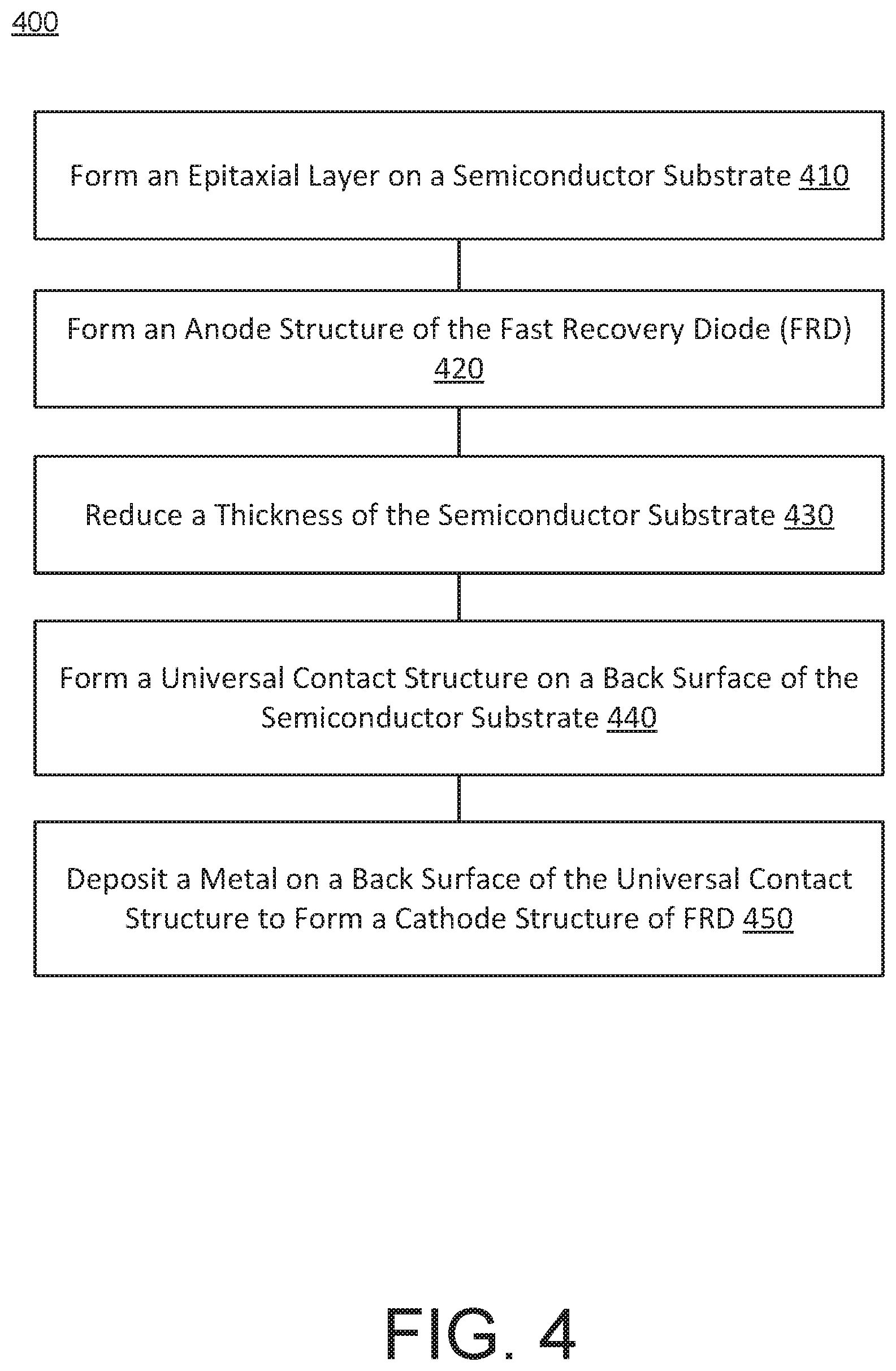
[0038] FIG. 4 illustrates a method 400 for fabricating an FRD (e.g., FRD 100) with soft recovery characteristics. FIGS. 5A-5F, which may be viewed in conjunction with FIGS. 1A and 1B (and FIG. 3), schematically illustrate a cross-sectional view of portions of a semiconductor substrate as it is being processed at different stages or steps of method 400 to make FRD 100.
[0039] As shown in FIG. 4, method 400 includes growing an n-type epitaxial layer on a N-type semiconductor substrate (e.g., an N+ doped silicon substrate) (410). The n-type epitaxial layer (which forms a drift region, e.g., semiconductor region 120 of FRD 100) may be undoped or lightly doped at a concentration lower than that of the N-type semiconductor substrate
[0040] Method 400 further includes forming an anode structure of the FRD (420). Forming the anode structure may include forming a P+ layer on a top surface of the n-type epitaxial layer and depositing a metal layer on the P+ layer to form an anode structure of FRD 100. The P+ layer may be formed by thermal diffusion, and/or implantation, of p dopant species into the top surface of the n-type epitaxial layer.
[0041] Method 400 further includes back grinding the semiconductor substrate to reduce its thickness (430). The reduced thickness of the back-ground semiconductor substrate may correspond to a thickness of a buffer layer of FRD 100.
[0042] Method 400 further includes forming a universal contact (e.g., universal contact structure 133) on a back surface of the back-ground semiconductor substrate (440). Forming the universal contact may involve a buffer implantation (e.g., of an n dopant such as phosphorus), followed by a p dopant (e.g., boron) implantation into the back surface of the back-ground semiconductor substrate. Forming the universal contact may further involve a photolithographic patterning step to delineate the P+ regions 134A and the N+ regions 134B of universal contact structure 133, followed by n dopant (e.g., phosphorus) implantation to form the N+ regions 134B. A laser annealing step may be carried out to activate the foregoing dopants in universal contact structure 133.
[0043] Method 400 further includes depositing a back metal on a back surface of universal contact structure 133 to form a cathode structure of FRD 100 (450).
[0044] In example implementations, where FRD 100 includes cathode structure 332 (shown in FIG. 3), forming a universal contact on a back surface of the back-ground semiconductor substrate 440 in method 400 may include patterning and depositing an oxide layer (e.g., oxide layer 336) over P+ region 134A and partially over N+ regions 134B. The oxide layer may be deposited before depositing the back metal on the back surface of universal contact structure 133.
[0045] As previously noted, FIGS. 5A-5F, schematically illustrate a cross-sectional view of portions of a semiconductor substrate as it is being processed at different stages or steps of method 400 to make FRD 100.
[0046] FIG. 5A shows, for example, a portion of a semiconductor substrate 510 that is being processed by method 400 to make FRD 100. In example implementations, semiconductor substrate 510 may be an N+ silicon wafer with resistivity in the range of about 0.001-50 .OMEGA.cm.
[0047] FIG. 5B shows, for example, at step 410 of method 400, an epitaxial layer 520 grown on semiconductor substrate 510. In example implementations, epitaxial layer 520 may be a undoped or lightly doped epitaxial layer with a resistivity, for example, in the range of 20-200 .OMEGA.cm and have a thickness, for example, in a range of about 10-100 .mu.m.
[0048] FIG. 5C shows, for example, at step 420 of method 400, formation of an anode structure 530 of FRD 100. Anode structure 530 may, for example, include a P+ layer 532 on a top surface of epitaxial layer 520 and a metal layer 534 deposited on the P+ layer 532.
[0049] FIG. 5D shows, for example, semiconductor substrate 510 with a reduced thickness T after it has been back ground at step 430 of method 400,
[0050] FIG. 5E shows, for example, at step 440 of method 400, formation of a universal contact 533 (having alternating P doped and N doped regions) on a backside of semiconductor substrate 510 with reduced thickness T.
[0051] FIG. 5F shows, for example, at step 450 of method 400, a back metal 535 deposited on a back surface of universal contact 533 to form a cathode structure 537 of FRD 100 (450).
[0052] FIG. 6A is a X-Y plot of a cross-section of diode 610 with a trace line C1 extending from a top of diode 610 to a bottom of diode 610. An example diode 610 may have a vertical die thickness t of about 0.114 millimeters and a lateral die area (e.g., in a plane perpendicular to FIG. 6A, not shown) of about 11 square millimeters. Diode 610 has a conventional cathode structure (i.e. without a backside p-n-junction). FIG. 6B is a X-Y plot illustrating dopant concentrations in diode 610 along trace line C1.
[0053] FIG. 7A is a X-Y plot of a cross-section of diode 710 with a trace line C1 extending from a top of diode 710 to a bottom of diode 710. An example diode 710 may have a universal contact including a N+ semiconductor region 712A and a P+ semiconductor region 722 forming a backside p-n junction 732. Diode 710 may have a vertical die thickness t of about 0.114 millimeters and a lateral die area (e.g., in a plane perpendicular to FIG. 7A, not shown) of about 11 square millimeters. FIG. 7B is a X-Y plot illustrating dopant concentrations in the universal contact region of diode 710 along trace line C1.
[0054] FIG. 8 is a graph illustrating simulated reverse recovery current 810 and voltage 830 for diode 610 (without a backside p-n junction), and reverse recovery current 820 and voltage 840 for diode 710 (with universal contact including a backside p-n junction in its cathode structure). The simulations were carried out using a Technology Computer-Aided Design (TCAD) tool with the diodes placed in an inductor-resistor circuit with the following parameters: diode area 11 mm2; die thickness 0.114 mms; reverse voltage (VR)=800 V; and forward current (IF)=40 A.
[0055] As seen in FIG. 8, on comparing reverse recovery current 820 and reverse recovery current 810, diode 710 (with a universal contact including a backside p-junction) exhibits a softer recovery than diode 610 (without a universal contact).
[0056] FIG. 9A shows simulated reverse recovery currents for a set of diodes having different p-to-n areal ratios in the universal contacts of the diodes. Reverse recovery current 910 corresponds to a diode having a universal contact p-to-n areal ratio of zero:200 (i.e., a diode without a universal contact); reverse recovery current 920 corresponds to a diode having a universal contact p-to-n areal ratio of 50:100; reverse recovery current 930 corresponds to a diode having a universal contact p-to-n areal ratio of 100:100; and reverse recovery current 940 corresponds to a diode having a universal contact p-to-n areal ratio of 150:100.
[0057] A portion of FIG. 9A is enclosed in dashed line rectangular box 97. FIG. 9B shows an exploded view of the portion of FIG. 9A is enclosed in the dashed line rectangular box 97.
[0058] In FIGS. 9A and 9B, an arrow 91 is overlaid across the reverse recovery current curves as a visual aid to indicate a direction of increasing p-to-n areal ratios (i.e., (zero:100 to 150:100) in the universal contacts of the diodes.
[0059] A length of a tail of the reverse current curve approaching zero is a measure of the softness of the reverse current recovery of the diode. As seen in FIGS. 9A and 9B, a tail 93 of the reverse recovery currents increases in length as the p-to-n areal ratios in the universal contacts of the diodes increase. Thus, increasing the p-to-n areal ratio in the universal contact of a diode is likely to increase softness of the reverse current recovery of the diode.
[0060] FIG. 10 shows simulated forward currents (IF) as a function of forward voltage (VF) for a set of diodes having different p-to-n areal ratios in the universal contacts of the diodes. Forward current 1010 corresponds to a diode having no universal contact (i.e., a diode without a universal contact); forward current 1020 corresponds to a diode having a universal contact p-to-n areal ratio of 50:150 (i.e., 0.33:1); forward current 1030 corresponds to a diode having a universal contact p-to-n areal ratio of 100:100 (i.e., 1:1); and forward current 1040 corresponds to a diode having a universal contact p-to-n areal ratio of 150:100 (i.e., 1.5:1).
[0061] FIG. 11 shows simulated reverse load currents (IR) as a function of load voltage (VR) for the same set of diodes as FIG. 10. Reverse load current 1110 corresponds to a diode having no universal contact p-to-n areal ratio (i.e., a diode without a universal contact); reverse load current 1120 corresponds to a diode having a universal contact p-to-n areal ratio of 50:150 (i.e., 0.33:1); reverse recovery current 1130 corresponds to a diode having a universal contact p-to-n areal ratio of 100:100 (i.e., 1:1); and reverse recovery current 1140 corresponds to a diode having a universal contact p-to-n areal ratio of 150:100 (i.e., 1.5:1).
[0062] An arrow 92 is overlaid across the forward current curves in FIG. 10 (and the reverse load current curves in FIG. 11) as a visual aid to indicate a direction of increasing p-to-n areal ratios (i.e., zero:200 to 150:100) in the universal contacts of the diodes.
[0063] As seen in FIG. 10, the forward voltages of the diodes increase as the p-to-n areal ratio in the universal contacts of the diode increases (e.g., from zero:200 to 150:50). However, as seen in FIG. 11, the reverse load current curves (1110, 1120, 1130, and 1140) for different p-to-n areal ratios are bunched up together and substantially overlap each over a voltage range of 1500V to 170V. Increases of the p-to-n areal ratios in the universal contacts of the diodes appear to have no effect on the breakdown voltages (Vbr) of the diodes (in other words, the breakdown voltages Vbr of the diodes do not appear to depend on the p-to-n areal ratios).
[0064] As noted previously (with reference to FIG. 3) the characteristics of the diodes can be further improved by including an oxide layer in the universal contacts. FIG. 12 shows a simulated reverse recovery current 1210 for a diode with no oxide layer included in its universal contact (which, e.g., has a p-to-n areal ratio of 75:25 (i.e., 3:1)). For comparison, FIG. 12 also shows a simulated reverse recovery current 1220 for a diode with an oxide layer covering the p-regions of its universal contact (which, e.g., has a p-to-n areal ratio of 50:50 (i.e., 1:1)).
[0065] FIG. 13 shows a simulated forward current 1310 for the diode with no oxide layer included in its universal contact (which, e.g., has a p-to-n areal ratio of 75:25 (i.e., 3:1)). For comparison, FIG. 13 also shows a simulated forward current 1320 for the diode with an oxide layer cover the p-regions of its universal contact (which, e.g., has a p-to-n areal ratio of 50:50 (i.e., 1:1)).
[0066] As seen in FIG. 12 (on comparison of current 1210 and current 1220), introducing the oxide layer in the universal contact results in a softer reverse current recovery in the diode. As seen in FIG. 13 (on comparison of current 1310 and current 1320), introducing the oxide layer in the universal contact results in a smaller forward current in the diode.
[0067] The simulated currents and voltages described above with reference to FIG. 6A through FIG. 13 demonstrate that incorporating a universal contact including a backside p-n junction in the cathode structure improves the soft reverse current recovery characteristics of the diode. Including an oxide layer over P-regions of the universal contact additionally improves reverse current recovery of the diode.
[0068] It will also be understood that when an element, such as a transistor or resistor, is referred to as being on, connected to, electrically connected to, coupled to, or electrically coupled to another element, it may be directly on, connected or coupled to the other element, or one or more intervening elements may be present. In contrast, when an element is referred to as being directly on, directly connected to or directly coupled to another element or layer, there are no intervening elements or layers present. Although the terms directly on, directly connected to, or directly coupled to may not be used throughout the detailed description, elements that are shown as being directly on, directly connected or directly coupled can be referred to as such. The claims of the application (if included) may be amended to recite exemplary relationships described in the specification or shown in the figures.
[0069] As used in this specification, a singular form may, unless definitely indicating a particular case in terms of the context, include a plural form. Spatially relative terms (e.g., over, above, upper, under, beneath, below, lower, and so forth) are intended to encompass different orientations of the device in use or operation in addition to the orientation depicted in the figures. In some implementations, the relative terms above and below can, respectively, include vertically above and vertically below. In some implementations, the term adjacent can include laterally adjacent to or horizontally adjacent to.
[0070] Implementations of the various techniques described herein may be implemented in (e.g., included in) digital electronic circuitry, or in computer hardware, firmware, software, or in combinations of them. Portions of methods also may be performed by, and an apparatus may be implemented as, special purpose logic circuitry, e.g., an FPGA (field programmable gate array) or an ASIC (application-specific integrated circuit).
[0071] Implementations may be implemented in a computing system that includes an industrial motor driver, a solar inverter, ballast, a general-purpose half-bridge topology, an auxiliary and/or traction motor inverter driver, a switching mode power supply, an on-board charger, an uninterruptible power supply (UPS), a back-end component, e.g., as a data server, or that includes a middleware component, e.g., an application server, or that includes a front-end component, e.g., a client computer having a graphical user interface or a Web browser through which a user can interact with an implementation, or any combination of such back-end, middleware, or front-end components. Components may be interconnected by any form or medium of digital data communication, e.g., a communication network. Examples of communication networks include a local area network (LAN) and a wide area network (WAN), e.g., the Internet.
[0072] While certain features of the described implementations have been illustrated as described herein, many modifications, substitutions, changes and equivalents will now occur to those skilled in the art. It is, therefore, to be understood that the appended claims are intended to cover all such modifications and changes as fall within the scope of the implementations. It should be understood that they have been presented by way of example only, not limitation, and various changes in form and details may be made. Any portion of the apparatus and/or methods described herein may be combined in any combination, except mutually exclusive combinations. The implementations described herein can include various combinations and/or sub-combinations of the functions, components and/or features of the different implementations described.
* * * * *
D00000
D00001
D00002
D00003
D00004
D00005
D00006
D00007
D00008
D00009
D00010
D00011
D00012

D00013

XML
uspto.report is an independent third-party trademark research tool that is not affiliated, endorsed, or sponsored by the United States Patent and Trademark Office (USPTO) or any other governmental organization. The information provided by uspto.report is based on publicly available data at the time of writing and is intended for informational purposes only.
While we strive to provide accurate and up-to-date information, we do not guarantee the accuracy, completeness, reliability, or suitability of the information displayed on this site. The use of this site is at your own risk. Any reliance you place on such information is therefore strictly at your own risk.
All official trademark data, including owner information, should be verified by visiting the official USPTO website at www.uspto.gov. This site is not intended to replace professional legal advice and should not be used as a substitute for consulting with a legal professional who is knowledgeable about trademark law.