Display Module, Display Panel, And Display Apparatus
OH; Pil Yong ; et al.
U.S. patent application number 16/935420 was filed with the patent office on 2021-02-11 for display module, display panel, and display apparatus. This patent application is currently assigned to SAMSUNG ELECTRONICS CO., LTD.. The applicant listed for this patent is SAMSUNG ELECTRONICS CO., LTD.. Invention is credited to Jeong In HAN, Sung Soo JUNG, Kwang Jae LEE, Pil Yong OH.
| Application Number | 20210043812 16/935420 |
| Document ID | / |
| Family ID | 1000004987124 |
| Filed Date | 2021-02-11 |


| United States Patent Application | 20210043812 |
| Kind Code | A1 |
| OH; Pil Yong ; et al. | February 11, 2021 |
DISPLAY MODULE, DISPLAY PANEL, AND DISPLAY APPARATUS
Abstract
The display panel includes: a panel cover; an adhesive layer positioned below the panel cover; and a plurality of display modules detachably attached to the panel cover by the adhesive layer. The adhesive layer includes: a first adhesive layer positioned on the plurality of display modules, and a second adhesive layer positioned on the first adhesive layer. A peel strength of the second adhesive layer is greater than a peel strength of the first adhesive layer.
| Inventors: | OH; Pil Yong; (Suwon-si, KR) ; LEE; Kwang Jae; (Suwon-si, KR) ; JUNG; Sung Soo; (Suwon-si, KR) ; HAN; Jeong In; (Suwon-si, KR) | ||||||||||
| Applicant: |
|
||||||||||
|---|---|---|---|---|---|---|---|---|---|---|---|
| Assignee: | SAMSUNG ELECTRONICS CO.,
LTD. Suwon-si KR |
||||||||||
| Family ID: | 1000004987124 | ||||||||||
| Appl. No.: | 16/935420 | ||||||||||
| Filed: | July 22, 2020 |
| Current U.S. Class: | 1/1 |
| Current CPC Class: | H01L 33/56 20130101; H01L 33/58 20130101; H01L 25/0753 20130101; G02B 1/14 20150115 |
| International Class: | H01L 33/56 20060101 H01L033/56; H01L 25/075 20060101 H01L025/075; H01L 33/58 20060101 H01L033/58; G02B 1/14 20060101 G02B001/14 |
Foreign Application Data
| Date | Code | Application Number |
|---|---|---|
| Aug 8, 2019 | KR | 10-2019-0096908 |
Claims
1. A display panel comprising: a panel cover; an adhesive layer provided below the panel cover; and a plurality of display modules detachably attached to the panel cover by the adhesive layer, wherein the adhesive layer comprises: a first adhesive layer provided on the plurality of display modules, and a second adhesive layer provided on the first adhesive layer, wherein a peel strength of the second adhesive layer is greater than a peel strength of the first adhesive layer.
2. The display panel according to claim 1, wherein the first adhesive layer is formed of one of silicon, acryl, polyvinyl alcohol, urethane, rubber, or any combination thereof.
3. The display panel according to claim 1, wherein the second adhesive layer is formed of one of silicon, acryl, polyvinyl alcohol, urethane, rubber, or any combination thereof.
4. The display panel according to claim 1, further comprising abase layer provided between the first adhesive layer and the second adhesive layer.
5. The display panel according to claim 4, wherein the base layer is formed of one of acryl, polyimide, or ultra-thin glass.
6. The display panel according to claim 1, further comprising an optical film provided on the panel cover.
7. The display panel according to claim 6, wherein a relationship of a thickness of the first adhesive layer and the second adhesive layer and a retardation satisfy a following inequality: a (nm)*.DELTA.n.ltoreq.b=10 nm, where a is the thickness of the first adhesive layer and the second adhesive layer, b is the retardation, and .DELTA.n represents a difference between a refractive index in a traveling direction of light and a refractive index in a direction that is perpendicular to the traveling direction of light.
8. The display panel according to claim 6, wherein a reflectivity of light transmitted through the adhesive layer is smaller than 0.5%.
9. The display panel according to claim 1, wherein the peel strength between each of the plurality of display modules and the first adhesive layer is in a range of 10 g/inch to 100 g/inch, and the peel strength between the panel cover and the second adhesive layer is in a range of 500 g/inch to 2,000 g/inch.
10. The display panel according to claim 1, wherein a thickness of the first adhesive layer and the second adhesive layer is in a range of 20 .mu.m to 200 .mu.m.
11. A display apparatus comprising: a frame; and a display panel installed in the frame, and comprising: a panel cover, a plurality of display modules detachably attached to the panel cover, and an adhesive layer, wherein the adhesive layer comprises: a first adhesive layer provided on the plurality of display modules, and a second adhesive layer provided on the first adhesive layer, wherein a peel strength of the second adhesive layer is greater than a peel strength of the first adhesive layer.
12. The display apparatus according to claim 11, wherein the first adhesive layer is formed of one of silicon, acryl, polyvinyl alcohol, urethane, rubber, or any combination thereof, and the second adhesive layer is formed of one of silicon, acryl, polyvinyl alcohol, urethane, rubber, or any combination thereof.
13. The display apparatus according to claim 11, wherein the peel strength between each of the plurality of display modules and the first adhesive layer is in a range of 10 g/inch to 100 g/inch, and the peel strength between the panel cover and the second adhesive layer is in a range of 500 g/inch to 2,000 g/inch.
14. The display apparatus according to claim 11, further comprising an optical film provided on the panel cover.
15. The display apparatus according to claim 11, further comprising: a rear cover covering a rear side of the frame; and a device board provided between the frame and the rear cover; and a panel board provided between the device board and the panel cover and electrically connected to the device board and the plurality of display modules.
16. The display apparatus according to claim 11, wherein the frame comprises: a frame body covering a rear side of the display panel; and an edge cover covering edges of the display panel.
17. A display module comprising: a substrate; a plurality of inorganic light emitting devices (ILEDs) mounted on an installation surface of the substrate; a first adhesive layer provided on each of the plurality of ILEDs; and a second adhesive layer provided on the first adhesive layer, wherein a peel strength of the second adhesive layer is greater than a peel strength of the first adhesive layer.
18. The display module according to claim 17, wherein the first adhesive layer is formed of one of silicon, acryl, polyvinyl alcohol, urethane, rubber, or any combination thereof.
19. The display module according to claim 17, wherein the second adhesive layer is formed of one of silicon, acryl, polyvinyl alcohol, urethane, rubber, or any combination thereof.
20. The display module according to claim 17, further comprising a base layer provided between the first adhesive layer and the second adhesive layer.
Description
CROSS-REFERENCE TO RELATED APPLICATION(S)
[0001] This application is based on and claims priority under 35 U.S.C. .sctn. 119 to Korean Patent Application No. 10-2019-0096908, filed on Aug. 8, 2019 in the Korean Intellectual Property Office, the disclosure of which is incorporated by reference herein in its entirety.
BACKGROUND
1. Field
[0002] The disclosure relates to a display module, a display panel, and a display apparatus, and more particularly, to a display apparatus having a display panel including a plurality of display modules on which a plurality of inorganic light emitting devices (ILEDs) are mounted.
2. Description of Related Art
[0003] A display apparatus visually displays images and data information, such as characters, figures, etc.
[0004] As a display apparatus, a liquid crystal panel, or an organic LED (OLED) panel formed by depositing OLEDs on a substrate has been widely used. However, the liquid crystal panel has a slow response time and high power consumption, and requires a backlight because the liquid crystal panel itself does not emit light. Accordingly, it is difficult to make a compact liquid crystal panel. Also, the OLED panel has a short life and a low mass production yield. For these reasons, as a new panel for replacing the light crystal panel and the OLED panel, a micro LED panel in which ILEDs are mounted on a substrate and the ILEDs themselves are used as pixels is being studied.
[0005] Because the micro LED panel does not require a backlight and minimizes a bezel, the micro LED panel may be reduced in size and thickness and is excellent in view of brightness, resolution, consumption power, and durability.
[0006] Also, because the micro LED panel does not require other complicated processes except for a process of picking up ILEDs from a wafer and transferring the ILEDs to a substrate, the micro LED panel may be manufactured to various resolutions and sizes according to consumers' orders and easily implemented as a large-size screen by assembling unit panel modules.
SUMMARY
[0007] Provided is a bezel-free display apparatus.
[0008] Also, provided are a display panel and a display apparatus capable of minimizing steps and/or gaps between a plurality of display modules.
[0009] Also, provided are a display panel and a display apparatus capable of easily replacing a display module of a plurality of display modules.
[0010] Additional aspects will be set forth in part in the description which follows and, in part, will be apparent from the description, or may be learned by practice of the presented embodiments.
[0011] In accordance with an aspect of the disclosure, a display panel includes: a panel cover; an adhesive layer positioned below the panel cover; and a plurality of display modules detachably attached to the panel cover by the adhesive layer, wherein the adhesive layer includes: a first adhesive layer positioned on the plurality of display modules; and a second adhesive layer positioned on the first adhesive layer, wherein peel strength of the second adhesive layer is greater than peel strength of the first adhesive layer.
[0012] The first adhesive layer may be formed of one of silicon, acryl, polyvinyl alcohol, urethane, rubber, and a combination thereof.
[0013] The second adhesive layer may be formed of one of silicon, acryl, polyvinyl alcohol, urethane, rubber, and a combination thereof.
[0014] The display panel may further include a base layer positioned between the first adhesive layer and the second adhesive layer.
[0015] The base layer may be formed of one of acryl, polyimide (PI), and ultra-thin glass (UTG).
[0016] The display panel may further include an optical film positioned on the panel cover.
[0017] The first adhesive layer and the second adhesive layer satisfy inequality (1): thickness of each adhesive layer (nm) *.rarw.n.ltoreq.10 nm, where .DELTA.n represents a difference between a refractive index in a traveling direction of light and a refractive index in a direction that is perpendicular to the traveling direction of light.
[0018] Reflectivity of light transmitting through the adhesive layer may be smaller than 0.5%.
[0019] Peel strength between the plurality of display modules and the first adhesive layer may be 10 g/inch to 100 g/inch, and peel strength between the panel cover and the second adhesive layer may be 500 g/inch to 2,000 g/inch.
[0020] A thickness of the first adhesive layer and the second adhesive layer may be 20 .mu.m to 200 .mu.m.
[0021] In accordance with an aspect of the disclosure, a display apparatus includes: a frame; and a display panel installed in the frame, and including a panel cover, a plurality of display modules detachably attached to the panel cover, and an adhesive layer, wherein the adhesive layer includes: a first adhesive layer positioned on the plurality of display modules; and a second adhesive layer positioned on the first adhesive layer, wherein peel strength of the second adhesive layer is greater than peel strength of the first adhesive layer.
[0022] The first adhesive layer may be formed of one of silicon, acryl, polyvinyl alcohol, urethane, rubber, and a combination thereof, and the second adhesive layer is formed of one of silicon, acryl, polyvinyl alcohol, urethane, rubber, and a combination thereof.
[0023] Peel strength between the plurality of display modules and the first adhesive layer may be 10 g/inch to 100 g/inch, and peel strength between the panel cover and the second adhesive layer may be 500 g/inch to 2,000 g/inch.
[0024] The display apparatus may further include an optical film positioned on the panel cover.
[0025] The display apparatus may further include: a rear cover covering a rear side of the frame; and a device board positioned between the frame and the rear cover, and electrically connected to a panel board.
[0026] The frame may include: a frame body covering a rear side of the display panel; and an edge cover covering edges of the display panel.
[0027] In accordance with an aspect of the disclosure, a display module includes: a substrate; a plurality of ILEDs mounted on an installation surface of the substrate; a first adhesive portion positioned on each of the plurality of ILEDs; and a second adhesive portion positioned on the first adhesive portion, wherein peel strength of the second adhesive portion is greater than peel strength of the first adhesive portion.
[0028] The first adhesive layer may be formed of one of silicon, acryl, polyvinyl alcohol, urethane, rubber, and a combination thereof.
[0029] The second adhesive portion may be formed of one of silicon, acryl, polyvinyl alcohol, urethane, rubber, and a combination thereof.
[0030] The display module may further include a base portion positioned between the first adhesive portion and the second adhesive portion.
BRIEF DESCRIPTION OF THE DRAWINGS
[0031] These and other aspects, features, and advantages of certain embodiments of the present disclosure will be more apparent from the following description taken in conjunction with the accompanying drawings, in which:
[0032] FIG. 1 shows an outer appearance of a display apparatus according to an embodiment;
[0033] FIG. 2 is an exploded perspective view showing main components of the display apparatus shown in FIG. 1;
[0034] FIG. 3 is a side cross-sectional view of a display module according to an embodiment;
[0035] FIG. 4 shows a portion of a cross section taken along line A-A' of FIG. 1;
[0036] FIG. 5 is an enlarged view of an adhesive layer of a display panel according to an embodiment;
[0037] FIG. 6 is an enlarged view of an adhesive layer of a display panel according to an embodiment;
[0038] FIG. 7 is a graph showing a relationship between retardation and reflectivity of an adhesive layer according to an embodiment; and
[0039] FIGS. 8A and 8B show examples of an assembly method and a rework method of a display panel according to an embodiment.
DETAILED DESCRIPTION
[0040] Embodiments described herein are only the examples, and embodiments may be implemented in several forms and may be variously modified.
[0041] It is to be understood that the singular forms "a," "an," and "the" include plural referents unless the context clearly dictates otherwise. In the drawings, for easy understanding, the shapes, sizes, etc. of components are more or less exaggeratedly shown.
[0042] It will be understood that when the terms "includes," "comprises," "including," and/or "comprising," when used in this specification, specify the presence of stated features, figures, steps, operations, components, members, or combinations thereof, but do not preclude the presence or addition of one or more other features, figures, steps, operations, components, members, or combinations thereof.
[0043] Throughout the disclosure, the expression "at least one of a, b or c" indicates only a, only b, only c, both a and b, both a and c, both b and c, all of a, b, and c, or variations thereof.
[0044] Hereinafter, the embodiments of the disclosure will be described in detail with reference to the accompanying drawings.
[0045] FIG. 1 shows an outer appearance of a display apparatus according to an embodiment. FIG. 2 is an exploded perspective view showing main components of the display apparatus shown in FIG. 1.
[0046] Referring to FIGS. 1 and 2, a display apparatus 1, which is an apparatus for displaying information and data as characters, figures, graphs, images, etc., may be a television (TV), a personal computer (PC), a mobile device, a digital signage, etc. The display apparatus 1 may be installed on a ground by a stand or on a wall.
[0047] According to an embodiment, the display apparatus 1 may include a display panel 100 for displaying images, a frame 20 supporting the display panel 100, and a rear cover 10 accommodating the display panel 100 and the frame 20. The display panel 100 installed in the frame 20 may implement a screen of the display apparatus 1.
[0048] The rear cover 10 may form a portion of the outer appearance of the display apparatus 1. The rear cover 10 may form an outer appearance of a rear side of the display apparatus 1. The rear cover 10 may cover a rear side of the frame 20.
[0049] The frame 20 may be made of a metal or a resin material to have stiffness. The frame 20 may have a nearly rectangular shape. The frame 20 may include a frame body 21 covering a rear side of the display panel 100, and an edge cover 22 formed at edges of the frame body 21. The edge cover 22 may extend toward a front direction of the display apparatus 1. The edge cover 22 may form upper, lower, and side outer appearances of the display apparatus 1. The display panel 100 may be accommodated in the frame 20 and supported by the frame 20.
[0050] The display apparatus 1 may include a device board 30 positioned between the frame 20 and the rear cover 10. The device board 30 may include a switching mode power supply for supplying power required for driving the display apparatus 1. The device board 30 may include a printed circuit board (PCB) for controlling images that are displayed on the display panel 100. The device board 30 may include a timing controller for adjusting an amount of data that is transmitted to a panel board 40 and improving image quality. The device board 30 may include a signal processing board for data processing.
[0051] The display apparatus 1 may include the panel board 40 positioned between the frame 20 and the display panel 100. The panel board 40 may control a plurality of display modules 110. The panel board 40 may be electrically connected to the plurality of display modules 110. In an embodiment, 8 panel boards 40 are provided, and the panel boards 40 are electrically connected to 8 display modules 110, respectively. However, an electrical connection structure of the panel board 40 and the plurality of display modules 110 is not limited to this. The panel board 40 may be electrically connected to the device board 30. The panel board 40 may receive power or data from the device board 30.
[0052] The display panel 100 may include the display modules 110, and a panel cover 120 positioned in front of the display modules 110. The display panel 100 may tile the display modules 110 on the panel cover 120 to implement a large screen. Details about coupling of the display modules 110 to the panel cover 120 will be described later.
[0053] Referring to FIG. 2, the display modules 110 may be arranged as an M*N matrix in up, down, left, and right directions to be adjacent to each other. In an embodiment, 64 display modules 110 may be arranged in as an 8.times.8 matrix on the frame 20. However, the number or arrangement of the display modules 110 are not limited to an embodiment, and may be set variously. The display modules 110 may have a flat shape or a curved shape. Also, the display modules 110 may have a variable curvature.
[0054] The display modules 110 may have the same configuration. Accordingly, descriptions about one display module 110 provided below may be applied to the other display modules 110.
[0055] The display module 110 according to an aspect of the disclosure may include a substrate 111, and one or more ILEDs 119 mounted on a front surface of the substrate 111. The front surface on which the ILEDs are mounted is also referred to as an installation surface 111a.
[0056] The substrate 111 may include a material, such as PI, FR4, glass, and the like. On the installation surface 111a of the substrate 111 on which the ILEDs are mounted, a pixel electrode, and a driving layer including a thin film transistor (TFT) may be formed. The substrate 111 may be a glass substrate. The substrate 111 may be a chip on class (COG) type substrate.
[0057] For example, the ILEDs 119a, 119b, and 119c may be formed of an inorganic material, such as silicon (Si), Sapphire, and/or gallium nitride (GaN). Because the ILEDs 119a, 119b, and 119c are more resistant to oxygen and water than OLEDs formed of an organic material, the ILEDs 119a, 119b, and 119c have a long life and excellent power efficiency.
[0058] The ILEDs 119a, 119b, and 119c may be picked up from a source wafer and mounted directly on the substrate 111. The ILEDs 119a, 119b, and 119c may be picked up and transferred through an electrostatic method using an electrostatic head, an adhesive method using an elastic polymer material, such as polydimethylsiloxane (PDMS) or silicon, as a head, laser ablation, Laser Lift Off (LLO), etc. A horizontal length, a vertical length, and a height of each of the ILEDs 119a, 119b, and 119c may be several micro meters (um) to several hundreds of micro meters.
[0059] Each of the ILEDs 119a, 119b, and 119c may include a p-n diode and a pair of element electrodes 113, and may be in a form of a flip chip in which the pair of element electrodes 113 are arranged toward the same direction. The pair of element electrodes 113 of the ILEDs 119a, 119b, and 119c may be connected to a pair of substrate electrodes 114 through soldering. However, the ILEDs 119a, 119b, and 119c may be a lateral or vertical type, and may be connected to the substrate electrodes 114 through wires.
[0060] Referring to FIG. 2, the ILEDs 119a, 119b, and 119c may include a red ILED 119a emitting red light, a green ILED 119b emitting green light, and a blue ILED 119c emitting blue light.
[0061] A red ILED 119a, a green ILED 119b, and a blue ILED 119c may form an ILED group. The group of ILEDs 119 may form a pixel. That is, the red ILED 119a, the green ILED 119b, and the blue ILED 119c may respectively form a red sub pixel, a green sub pixel, and a blue sub pixel, which together form one pixel.
[0062] In FIG. 2, an example in which the red ILED 119a, the green ILED 119b, and the blue ILED 119c are arranged in a line is shown. However, the red ILED 119a, the green ILED 119b, and the blue ILED 119c may be arranged to form a triangle shape or any other shapes.
[0063] A plurality of ILED groups may be arranged at regular intervals. An interval between the ILED groups may be set variously according to a resolution and size of the display apparatus 1.
[0064] On the substrate 111, a black layer may be formed to absorb light between the ILEDs 119a, 119b, and 119c. On the substrate 111, an encapsulation layer may be formed to protect the ILEDs 119a, 119b, and 119c. The encapsulation layer may be formed on the substrate 111 to cover the ILEDs 119a, 119b, and 119c. The encapsulation layer may be formed of a resin, such as silicon, urethane, epoxy, acryl, and the like, or may be formed of optically clear adhesive (OCA), optically clear resin (OCR), etc. The encapsulation layer may include a viscoelastic material of which viscoelasticity and stiffness change according to a change of temperature or pressure, to physically sufficiently protect the ILEDs 119a, 119b, and 119c and improve image quality. The viscoelastic material may include at least one of silicon, urethane, epoxy, or an acrylic compound.
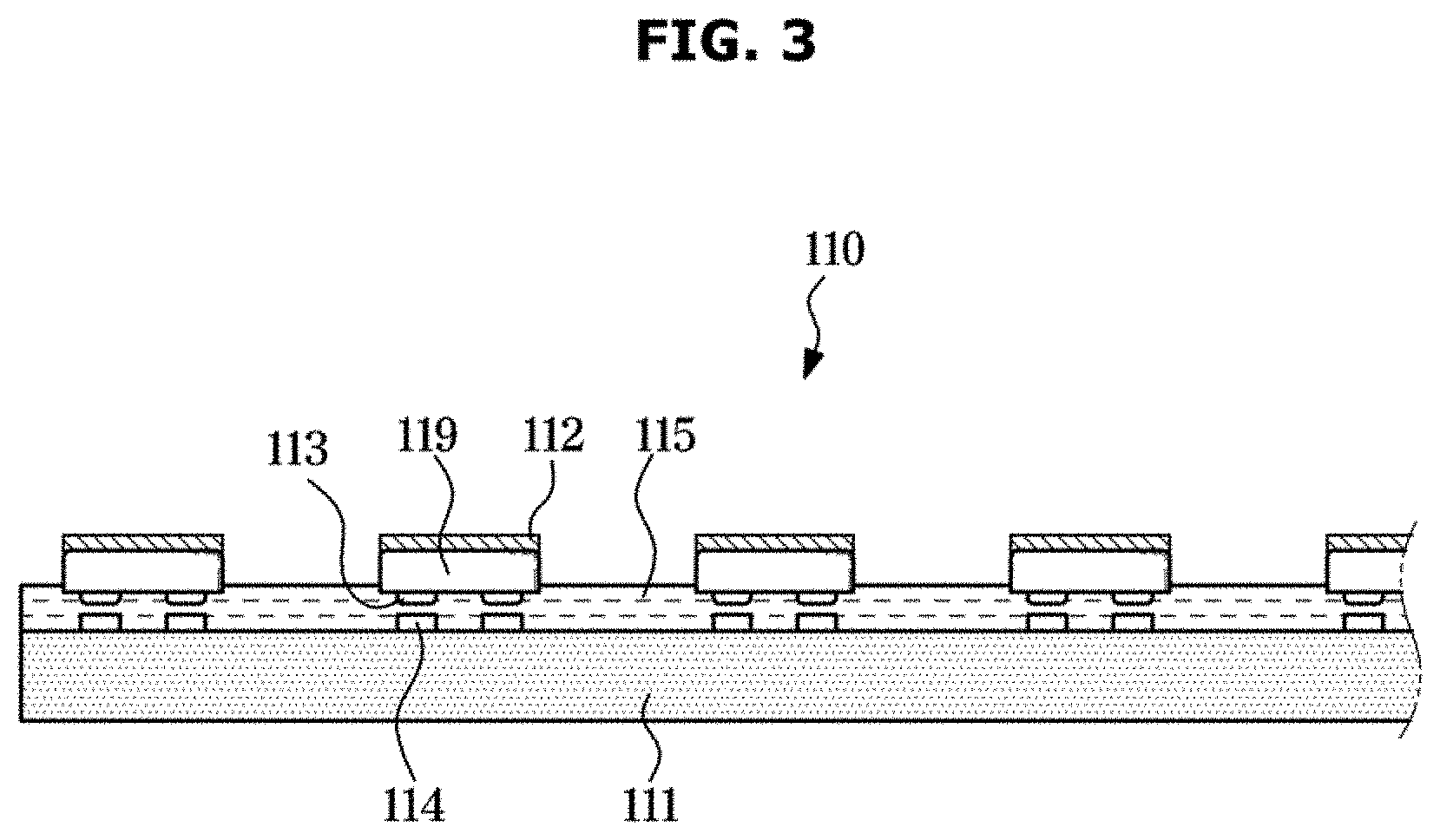
[0065] FIG. 3 is a side cross-sectional view of the display module 110 according to an embodiment.
[0066] Referring to FIG. 3, on the substrate 111, the pair of substrate electrodes 114 electrically connected to the pair of element electrodes 113 may be provided.
[0067] To electrically connect the ILEDs 119 to the substrate 111, a conductive bonding layer 115 may be formed on the substrate 111. The conductive bonding layer 115 may be formed on the entire area of the substrate 111. The conductive bonding layer 115 may enable electrical connections between the pair of element electrodes 113 and the pair of substrate electrodes 114.
[0068] As such, by electrically connecting the element electrodes 113 of the ILEDs 119 to the substrate electrodes 114 of the substrate 111 by using the conductive bonding layer 115, the ILEDs 119 may be prevented from being damaged during a bonding process, reliability of bonding may be improved, and a bonding process may be simplified.
[0069] According to an embodiment, the display module 110 may further include an adhesive portion 112 of a transparent material formed on each of the ILEDs 119.
[0070] In the related art, a display panel is attached to a panel cover by using an OCA which is a single layer. However, it is difficult to separate the display panel from the panel cover due to a strong adhesive force of the OCA when a display apparatus needs to be reworked due to a panel defect after the display apparatus is manufactured and assembled.
[0071] According to an embodiment, by applying the adhesive portion 112 of the transparent material on the ILEDs 119 of the display module 110, that is, in a light-emitting direction, the display panel 100 may be adhered to the panel cover 120 with a level of an adhesive force by which the display panel 100 is separable from the panel cover 120. More specifically, because the adhesive portion 112 has a relatively strong adhesive force with respect to the panel cover 120 and a relatively weak adhesive force with respect to the ILEDs 119, reworking may be allowed and a separation force may be significantly reduced, resulting in high reworking efficiency.
[0072] According to an embodiment, the adhesive portion 112 may include a first adhesive portion provided on each of the ILEDs 119, and a second adhesive portion provided on the first adhesive portion and having greater peel strength than that of the first adhesive portion. That is, the adhesive portion 112 may be configured with the first adhesive portion and the second adhesive portion and attached to the ILED 119 of the display module 110. The first adhesive portion and the second adhesive portion may have a shape corresponding to that of the ILED 119.
[0073] The first adhesive portion may be formed on the ILED 119 of the display module 110. The first adhesive portion may be formed of an optically isotropic material which is any one of silicon, acryl, polyvinyl alcohol, urethane, rubber, and a combination thereof.
[0074] The second adhesive portion may be provided on the first adhesive portion. The second adhesive portion may be formed of a material having relatively greater peel strength than the first adhesive portion. For example, the second adhesive portion may be formed of an optically isotropic material which is any one of silicon, acryl, polyvinyl alcohol, urethane, rubber, and a combination thereof.
[0075] The first adhesive portion and the second adhesive portion may have a thickness of 10 .mu.m to 60 .mu.m. When the thickness of the adhesive portion 112 is too thick, it may be difficult to ensure a viewing angle when surface treatment such as printing a black pattern is performed on the panel cover 120 as necessary, and also it may be difficult to ensure price competitiveness. Also, when the thickness of the adhesive portion 112 is too thin, it may be difficult to ensure strength so that the adhesive portion 112 may be easily torn.
[0076] A method of attaching the first adhesive portion and the second adhesive portion to the ILEDs 119 of the display module 110 may be implemented by forming a film, a molding, etc. having adhesion on the display module 110, although not limited thereto. However, the method may be performed by using any method known to those skilled in the art.
[0077] The adhesive portion 112 of the transparent material configured with the first adhesive portion and the second adhesive portion described above may be formed on some of the ILEDs 119 in consideration of an adhesive force with the display module 110.
[0078] The display module 110 according to an embodiment may further include a base portion between the first adhesive portion and the second adhesive portion. The base portion may have a shape corresponding to the first adhesive portion and the second adhesive portion.
[0079] By applying the base portion between the first adhesive portion and the second adhesive portion, a relatively strong adhesive force with respect to the panel cover 120 and a relatively weak adhesive force with respect to the ILEDs 119 may be achieved.
[0080] The base portion may be formed of an optically isotropic material which is any one of acryl, PI and UTG. A thickness of the base portion may be 40 .mu.m or more in consideration of an adhesive force and stability with the first adhesive portion and the second adhesive portion.
[0081] For example, by performing surface treatment on both surfaces of an adhesive layer, the second adhesive portion may be formed on the base portion and the first adhesive portion may be formed below the base portion.
[0082] The surface treatment for forming the first adhesive portion and the second adhesive portion on both surfaces of the base portion is not limited, and may be chemical treatment or mechanical etching known to those skilled in the art. For example, the chemical treatment may be primer treatment using urethane, silicon, etc., and the mechanical etching may be corona discharge treatment or gas plasma treatment using oxygen, argon, ozone, etc.
[0083] The display panel 100 according to an embodiment may include the panel cover 120, and the plurality of display modules 110 detachably attached to the panel cover 120.
[0084] FIG. 4 shows a portion of a cross section taken along line A-A' of FIG. 1.
[0085] Referring to FIG. 4, the panel cover 120 for protecting and supporting the plurality of display modules 110 may be attached to the front surfaces of the display modules 110. The panel cover 120 may include glass. An adhesive layer 130 of a transparent material may be provided between the display modules 110 and the panel cover 120 and may be similar to the adhesive portion 112. Accordingly, the display modules 110 may be detachably attached to the panel cover 120.
[0086] According to an embodiment, by applying the adhesive layer 130 to the display modules 110, the display panel 100 may be adhered to the panel cover 120 with a level of an adhesive force by which the display panel 100 is separable from the panel cover 120.
[0087] More specifically, because the adhesive layer 130 has a relatively strong adhesive force with respect to the panel cover 120 and a relatively weak adhesive force with respect to the display modules 110, reworking may be allowed and a separation force may be significantly reduced, resulting in high reworking efficiency.
[0088] Accordingly, an adhesive force between the adhesive layer 130 and the panel cover 120 may be greater than an adhesive force between the adhesive layer 130 and the display module 110, which gives an effect of satisfying a separation force upon reworking while maintaining a coupling force between the display modules 110 and the panel cover 120.
[0089] FIG. 5 is an enlarged view of the adhesive layer 130 of the display panel 100 according to an embodiment.
[0090] According to an embodiment, the adhesive layer 130 of the transparent material may include a first adhesive layer 131 formed on the display modules 110, and a second adhesive layer 132 formed on the first adhesive layer 131 and having greater peel strength than the first adhesive layer 131. That is, the adhesive layer 130 may be configured with the first adhesive layer 131 and the second adhesive layer 132 and attached to the display modules 110. The first adhesive layer 131 and the second adhesive layer 132 may have a shape corresponding to that of the panel cover 120. For example, the first adhesive layer 131 and the second adhesive layer 132 may be a film, a molding, etc., although not limited thereto.
[0091] Also, the adhesive layer 130 may have a relatively weak adhesive force with respect to the panel cover 120 and a relatively strong adhesive force with respect to the display modules 110.
[0092] The first adhesive layer 131 may be formed on the display modules 110. The first adhesive layer 131 may be formed of an optically isotropic material which is any one of silicon, acryl, polyvinyl alcohol, urethane, rubber, and a combination thereof.
[0093] The second adhesive layer 132 may be formed on the first adhesive layer 131 of a material having greater peel strength than the first adhesive layer 131. For example, the second adhesive layer 132 may be formed of an optically isotropic material which is any one of silicon, acryl, polyvinyl alcohol, urethane, rubber, and a combination thereof.
[0094] The first adhesive layer 131 and the second adhesive layer 132 may have a thickness a of 20 .mu.m or more. For example, the first adhesive layer 131 and the second adhesive layer 132 may have a thickness a of 20 .mu.m to 200 .mu.m. The thickness of the first adhesive layer 131 and the second adhesive layer 132 may be selected according to strength of the display modules 110. When the thickness of the first adhesive layer 131 and the second adhesive layer 132 increases, it may be possible to increase the radius of curvature in a reworking process, which improves workability. However, when the thickness of the first adhesive layer 131 and the second adhesive layer 132 is too thin, it may be difficult to ensure strength, so that the first adhesive layer 131 and the second adhesive layer 132 may be easily torn.
[0095] FIG. 6 is an enlarged view of an adhesive layer of a display panel according to another embodiment.
[0096] The display panel 100 according to an embodiment may further include a base layer 133 between the first adhesive layer 131 and the second adhesive layer 132. The base layer 133 may have a shape corresponding to that of the first adhesive layer 131 and the second adhesive layer 132.
[0097] By applying the base layer 133 between the first adhesive layer 131 and the second adhesive layer 132, a relatively strong adhesive force with respect to the panel cover 120 and a relatively weak adhesive force with respect to the display modules 110 may be achieved.
[0098] The base layer 133 may be formed of an optically isotropic material which is any one of acryl, PI, and UTG. A thickness of the base layer 133 may be 40 .mu.m or more in consideration of an adhesive force and stability with the first adhesive layer 131 and the second adhesive layer 132.
[0099] For example, by performing surface treatment on both surfaces of the base layer 133, the second adhesive layer 132 may be formed on the base layer 133 and the first adhesive layer 131 may be formed below the base layer 133.
[0100] The surface treatment for forming the first adhesive layer 131 and the second adhesive layer 132 on both surfaces of the base layer 133 is not limited, and may be chemical treatment or mechanical etching known to those skilled in the art. For example, the chemical treatment may be primer treatment using urethane, silicon, etc., and the mechanical etching may be corona discharge treatment or gas plasma treatment using oxygen, argon, ozone, etc.
[0101] When the panel cover 120 is formed of glass, peel strength between the display modules 110 and the first adhesive layer 131 may be 10 g/inch to 100 g/inch, and peel strength between the panel cover 120 and the second adhesive layer 132 may be 500 g/inch to 2,000 g/inch.
[0102] The peel strength is the measure of the average force to part two bonded materials. For example, the strength may be calculated during a peel test at a constant speed rate and measured as the average load per unit.
[0103] Referring to FIGS. 5 and 6, by applying the adhesive layer 130 having different adhesive forces with respect to the display modules 110 and the panel cover 120, a coupling force between the display modules 110 and the panel cover 120 may be maintained uniform over the entire area of the display modules 110, and the panel cover 120 may be easily separated in an up-down direction from the display modules 110 upon reworking, thereby preventing a quality defect that the display panel 100 lifts.
[0104] According to an embodiment, the display panel 100 may further include an optical film formed on the panel cover 120 to improve optical performance. As the optical film, a circular polarizing film, a linear polarizing film, a retardation film, an antiglare (AG) film, a low-reflection (LR) film, an antireflective (AR) film, a hard-coating (HC) film, a neural density (ND) film, any combination thereof, etc. may be used alone or in combination through stacking of two or more films, to improve image quality. Also, surface treatment such as printing a black pattern may be performed on the panel cover 120.
[0105] For example, polyethylene terephthalate (PET), which is the base layer 133 used in the adhesive layer 130 for adhesion between the panel cover 120 and the display modules 110, may have optical anisotropy by a stretching process.
[0106] When the adhesive layer 130 applied between the display modules 110 and the panel cover 120 has optical anisotropy, retardation may occur in light passing through the adhesive layer 130. For example, when light having a wavelength of 550 nm is transmitted through a PET film having a thickness of 10 .mu.m, a path difference corresponding to 3.6 .lamda. (wavelength) may be generated. Accordingly, light distortion may occur, which disables the adhesive layer 130 to function as an optical film.
[0107] Inventors of the present disclosure have deduced retardation b that is expressed by the following inequality (1), by providing the adhesive layer 130 formed of the isotropic material (i.e., the isotropic adhesive layer) and considering the thickness of the adhesive layer 130 and a visible light wavelength range of 400 nm to 700 nm. The isotropic adhesive layer 130 may be a film in which a refractive index in a fast axis direction, a reflective index in a slow axis direction, and a reflective index in a thickness direction are in a substantially equivalent range.
[0108] According to an embodiment, the first adhesive layer 131 and the second adhesive layer 132 constituting the adhesive layer 130 of the display panel 100 may satisfy inequality (1) below.
[0109] Inequality (1): a (nm)*.DELTA.n.ltoreq.b=10 nm,
[0110] where a is an overall thickness of the adhesive layer,
[0111] b is a retardation to be equal to or less than 10 nm, and
[0112] .DELTA.n represents a difference between a refractive index in a traveling direction of light and a refractive index in a direction that is perpendicular to the traveling direction of light.
[0113] FIG. 7 is a graph showing a relationship between retardation and reflectivity of the adhesive layer 130 according to an embodiment.
[0114] Referring to FIG. 7, when retardation of light transmitted through the adhesive layer 130 is controlled to be smaller than or equal to 10 nm, reflectivity that is smaller than 0.5% is deduced. Accordingly, it is confirmed that the adhesive layer 130 functions as an optical film.
[0115] To control the retardation of light to be smaller than or equal to 10 nm, the adhesive layer 130 may be formed of an isotropic material which is any one of silicon, acryl, polyvinyl alcohol, urethane, rubber, and a combination thereof. For example, the first adhesive layer 131 and the second adhesive layer 132 may be formed of any one of colorless and transparent PI (CPI), pressure sensitive adhesive (PSA) acryl, polyester, poly carbonate, cyclo olefin polymer (COP), casting polypropylene (CPP), and glass.
[0116] According to an embodiment, because the display panel 100 includes the adhesive layer 130 formed as the isotropic adhesive layer, retardation of light transmitted through the adhesive layer 130 may be reduced. For example, light transmitted through the adhesive layer 130 may have retardation of about 10 nm or less.
[0117] Accordingly, the display panel 100 according to an embodiment does not cause performance deterioration such as light distortion even when an optical film is further formed on the panel cover 120.
[0118] FIGS. 8A and 8B show examples of an assembly method and a rework method of the display panel 100 according to an embodiment.
[0119] Referring to FIG. 8A, by attaching the panel cover 120 including the adhesive layer 130 to the plurality of display modules 110, the display panel 100 may be assembled.
[0120] The display apparatus 1 according to an embodiment may be configured to allow, when a display module of the plurality of display modules 110 needs to be replaced, easy replacement of the display module.
[0121] More specifically, referring to FIG. 8B, when a defect is generated in a display module of the plurality of display modules 110 so that reworking is needed, a worker may first separate the panel cover 120 of the display apparatus 1 from the display modules 110.
[0122] Because an adhesive force between the adhesive layer 130 and the display modules 110 is weaker than an adhesive force between the adhesive layer 130 and the panel cover 120, the worker may separate the panel cover 120 from the display modules 110 in a state in which the adhesive force between the adhesive layer 130 and the panel cover 120 is maintained, thereby increasing reworking efficiency of the display apparatus 1 having a small area.
[0123] Because the display apparatus 1 according to an embodiment includes the display panel 100 in which the plurality of display modules 110 are installed on the panel cover 120, a front chassis for supporting the display modules 110 may be omitted. That is, because the panel cover 120 supporting the display modules 110 is supported by the frame 20, the display apparatus 1 according to an embodiment may minimize a bezel. That is, the display apparatus 1 according to an embodiment may be implemented as a bezel-free type.
[0124] In addition, because the display apparatus 1 according to an embodiment adopts a front side direct attachment method in which the display modules 110 are installed on the panel cover 120, the display apparatus 1 may minimize steps between modules.
[0125] According to an embodiment, because the display apparatus attaches the plurality of display modules to the panel cover, a bezel for assembling and/or holding the display modules may be omitted.
[0126] According to an embodiment, because the display panel and the display apparatus integrate the display panel by attaching the plurality of display modules to the panel cover, steps and/or gaps between the display modules may be reduced.
[0127] According to an embodiment, because the display panel and the display apparatus allow easy separation in up-down direction of the display modules and the panel cover, reworking efficiency may increase.
[0128] While embodiments have been particularly shown and described with reference to the drawings, the embodiments are provided for the purposes of illustration and it will be understood by one of ordinary skill in the art that various modifications and equivalent other embodiments may be made from the disclosure. Accordingly, the true technical scope of the disclosure is defined by the technical spirit of the appended claims.
* * * * *
D00000
D00001
D00002
D00003
D00004
D00005
D00006
D00007
D00008
D00009
XML
uspto.report is an independent third-party trademark research tool that is not affiliated, endorsed, or sponsored by the United States Patent and Trademark Office (USPTO) or any other governmental organization. The information provided by uspto.report is based on publicly available data at the time of writing and is intended for informational purposes only.
While we strive to provide accurate and up-to-date information, we do not guarantee the accuracy, completeness, reliability, or suitability of the information displayed on this site. The use of this site is at your own risk. Any reliance you place on such information is therefore strictly at your own risk.
All official trademark data, including owner information, should be verified by visiting the official USPTO website at www.uspto.gov. This site is not intended to replace professional legal advice and should not be used as a substitute for consulting with a legal professional who is knowledgeable about trademark law.