Transition From A Stripline To A Waveguide
TRUMMER; Stefan
U.S. patent application number 16/640782 was filed with the patent office on 2021-02-04 for transition from a stripline to a waveguide. The applicant listed for this patent is ASTYX GmbH. Invention is credited to Stefan TRUMMER.
| Application Number | 20210036394 16/640782 |
| Document ID | / |
| Family ID | 1000005194595 |
| Filed Date | 2021-02-04 |


| United States Patent Application | 20210036394 |
| Kind Code | A1 |
| TRUMMER; Stefan | February 4, 2021 |
TRANSITION FROM A STRIPLINE TO A WAVEGUIDE
Abstract
The invention relates to a transition from a stripline to a waveguide, wherein: the stripline, preferably a microstrip line, is located on a substrate; an upper side of the substrate has a metallised surface and the lower side of the substrate has a metal layer, preferably a high-frequency ground-potential layer; the upper side and the lower side are connected to vias; and at least part of the metallised surface on the upper side of the substrate acts as a waveguide wall.
| Inventors: | TRUMMER; Stefan; (Oberhaching, DE) | ||||||||||
| Applicant: |
|
||||||||||
|---|---|---|---|---|---|---|---|---|---|---|---|
| Family ID: | 1000005194595 | ||||||||||
| Appl. No.: | 16/640782 | ||||||||||
| Filed: | August 20, 2018 | ||||||||||
| PCT Filed: | August 20, 2018 | ||||||||||
| PCT NO: | PCT/EP2018/072450 | ||||||||||
| 371 Date: | February 21, 2020 |
| Current U.S. Class: | 1/1 |
| Current CPC Class: | H01P 3/08 20130101; H01P 5/08 20130101; H05K 1/0237 20130101; H01P 3/12 20130101; H05K 1/115 20130101 |
| International Class: | H01P 5/08 20060101 H01P005/08; H01P 3/08 20060101 H01P003/08; H01P 3/12 20060101 H01P003/12; H05K 1/02 20060101 H05K001/02; H05K 1/11 20060101 H05K001/11 |
Foreign Application Data
| Date | Code | Application Number |
|---|---|---|
| Aug 24, 2017 | DE | 10 2017 214 871.3 |
Claims
1. A device comprising: a stripline situated on a substrate; a waveguide; and a transition from the stripline to the waveguide, wherein a top side of the substrate has a metallized surface and an underside of the substrate has a metal layer, wherein the top side and the underside are connected to vias, and wherein the waveguide comprises a wall at least partly formed by the metallized surface on the top side of the substrate.
2. The device as claimed in claim 1, wherein the stripline is contacted by a steplike structure connected to the waveguide.
3. The device as claimed in claim 2, wherein the steplike structure is situated within a block that comprises of metal or is metallized, and the block comprises a plurality of waveguide structures, and wherein at least a plurality of vias contact the block in a transition region.
4. The device as claimed in claim 3, wherein the block comprises a rectangular waveguide configured to propagate an electrical wave, and wherein the device is configured, during operation, to guide the electrical wave further within the block through a 90.degree. bend, wherein the wall of the waveguide is disposed only in the transition region.
5. The device as claimed in claim 4, wherein the 90.degree. bend is situated perpendicular to the substrate.
6. The device as claimed in claim 3, wherein the block comprises a plurality of milled layers 3D printed layers, and/or plastic injection-molded layers.
7. The device as claimed in claim 1, wherein the metal layer comprises a radio frequency ground potential layer.
8. The device as claimed in claim 2, wherein stripline is contacted by the steplike structure connected to the waveguide in a vicinity of the metallized surface on the top side of the substrate.
9. The device as claimed in claim 3, wherein at least the plurality of vias directly contact the block in the transition region.
Description
[0001] The present invention relates to a transition from a stripline to a waveguide. The transition is implemented by virtue of the fact that the stripline is situated on a substrate, wherein a top side of the substrate has a metallized surface and the underside of the substrate has a metal layer, wherein the top side and the underside are connected to vias, wherein the metallized surface on the top side of the substrate at least partly functions as a waveguide wall.
[0002] Increased requirements made of sensor technology as provided in the field of radar, for example, owing to the objective of autonomous driving are giving rise to new challenges in sensor development. These increased demands have to be taken into account here primarily in the case of the antennas of the sensors, since these have a crucial influence on the overall system. In this case, planar antennas situated on printed circuit boards, these antennas frequently being used at the present time, are often no longer able to provide the necessary power. Therefore, waveguide antennas are increasingly being used. Since other sensor components, such as receiver and transmission chips, for example, are still situated on printed circuit boards, suitable transitions between waveguiding elements on printed circuit boards and waveguiding elements in a waveguide are crucial components of many new sensor systems.
[0003] The document DE 196 36 890 C1 describes a method that includes contacting a stripline with a web situated in the waveguide. In this case, the contacting of the waveguide walls is effected both above and below the substrate. However, this principle has the serious disadvantage that such transitions can be situated only at the edge of a substrate.
[0004] On account of the increased requirements made of the sensor systems, in the future it will be necessary to distribute transitions on the substrate.
[0005] It is therefore an object of the present invention to provide a transition from a stripline to a waveguide which eliminates or reduces the disadvantages present in the prior art and realizes required line routing.
[0006] The stated object is achieved in accordance with the features of independent patent claim 1 in that the stripline is situated on a substrate, wherein a top side of the substrate has a metallized surface and the underside of the substrate has a metal layer, wherein the top side and the underside are connected to vias, wherein the metallized surface on the top side of the substrate at least partly functions as a waveguide wall.
[0007] One advantage here is that the transitions can be realized flexibly at any desired locations on a substrate, with the result that required line routings are achieved. A further advantage is that an optimized construction and an improved power are realized.
[0008] Preferred or advantageous embodiments of the invention are evident from the dependent claims, the following description and also the accompanying figures.
[0009] Preferably, the stripline is contacted by a steplike structure connected to the waveguide, preferably in the vicinity of the metallized surface on the top side of the substrate.
[0010] Preferably, the structure is situated within a block that consists of metal or is metallized, and the block has a plurality of waveguide structures, wherein at least a plurality of vias, preferably directly, contact the block in a transition region.
[0011] Preferably, the block has a rectangular waveguide in which an electrical wave propagates, wherein the waveguide wave is guided further within the block by means of a 90.degree. bend, such that the metallized surface on the top side of the substrate functions as a waveguide wall only in the transition region.
[0012] The 90.degree. bend is preferably situated perpendicular to the substrate.
[0013] Preferably, the block has a plurality of layers produced by means of milling technology and/or 3D printing technology and/or plastic injection-molding methods. Furthermore, a transition can be produced by means of an embossing or diecasting or cold flow process with subsequent metallization.
[0014] Preferably, the stripline ends at the location at which it is contacted by the structure connected to the waveguide.
[0015] The block usually consists of metal or of some other material which is metallized, and can be produced in different layers connected to one another. The necessary design criteria such as adding radii and drafts or possible design criteria can be provided without any problems for the block. Furthermore, the steplike contact structure can also be embodied in the form of one or more chamfers.
[0016] Further features, advantages and effects of the invention are evident from the following description of exemplary embodiments and the accompanying figures, in which:
[0017] FIG. 1 shows a basic construction of a transition;
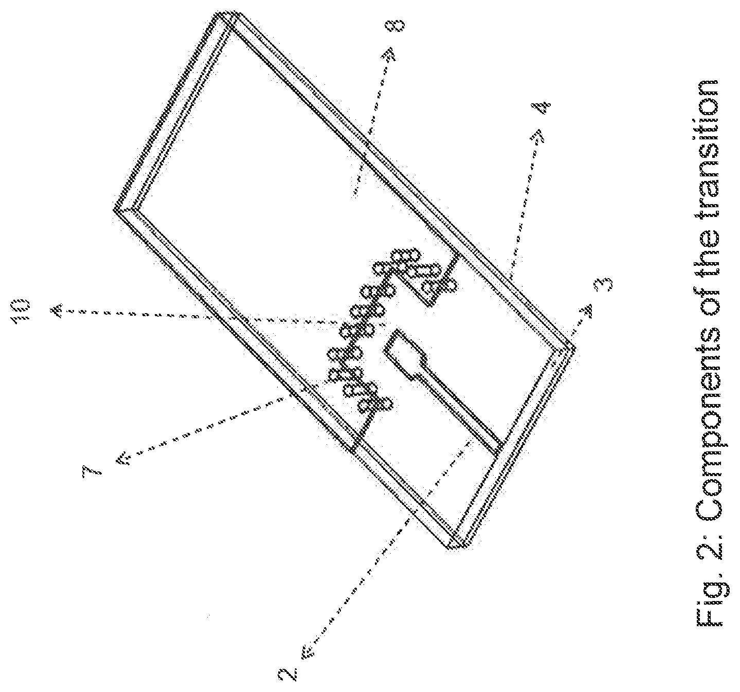
[0018] FIG. 2 shows components of a transition which are situated directly at a substrate;
[0019] FIG. 3 shows components of a transition which are situated within a block;
[0020] FIG. 4 shows exemplary further guidance of the waveguide wave in a block; and
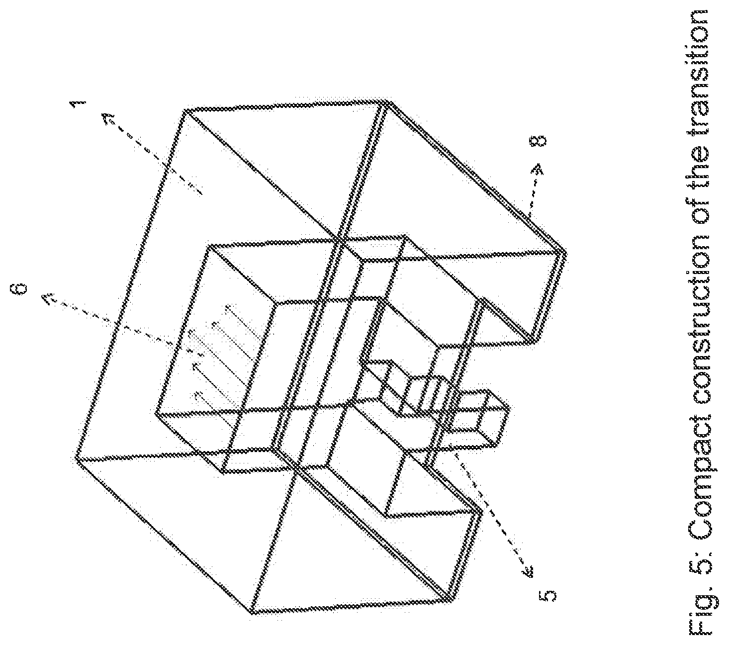
[0021] FIG. 5 shows a compact embodiment of a transition, illustrating exclusively a block with a waveguide structure and a ground surface on a substrate.
[0022] FIG. 1 shows a basic construction of a transition, consisting of a microstrip line. The microstrip line 2 is situated on a substrate 3. A layer 4 at radio-frequency ground potential is situated below the substrate. The known fundamental mode of the microstrip line 2, a so-called quasi-transverse electromagnetic (quasi-TEM) mode, thus forms. The microstrip line 2 is then contacted by a steplike structure 5. The microstrip line mode is thus transformed to an H10 rectangular waveguide mode 6. The steplike contact structure 5 is situated within a block 1 that includes all the waveguide structures. The contact structure 5 is connected to a waveguide wall. The transition in accordance with FIG. 1 thus consists of:
[0023] a block 1 having waveguide structures,
[0024] a rectangular waveguide 6 with H10 wave,
[0025] a metallized surface 8 on the substrate,
[0026] vias 7,
[0027] a layer 4 at ground potential,
[0028] a substrate 3,
[0029] a microstrip line 2 with wave in the fundamental mode, and
[0030] a steplike structure 5 that contacts the microstrip line.
[0031] The radio-frequency ground potential required for the microstrip line mode is transferred from a metal layer on the underside of the substrate to the metallized surface on the top side of the substrate by virtue of the fact that both surfaces are connected to vias in the region of the steplike contact structure. In this case, the metallized surface on the substrate partly functions as a wall of the waveguide. The other waveguide walls are situated in the block. They obtain their radio-frequency ground potential by virtue of the fact that some vias that transfer the ground potential directly contact the block in the transition region. This construction ensures that transitions can be realized flexibly at any desired locations on the substrate.
[0032] FIG. 2 shows the components of a transition which are situated directly at the substrate 3. Said components are the microstrip line 2, a metallized surface 8 on the substrate, and a layer 4 at ground potential below the substrate 3. In this case, the microstrip line 2 has a widened portion at its end. The metallized surface 8 on the substrate begins shortly before the end of the microstrip line, wherein a surface having no metallization is situated between the metallized surface and the end of the microstrip line. This region is referred to as a cutout 10 of the metallized surface. Along said cutout 10, the metallized surface 8 on the substrate 3 is connected to a layer 4 at ground potential situated below the substrate 3, by means of vias 7.
[0033] FIG. 3 shows a block 1 having a waveguide structure, said block being situated above the substrate. Said block has a rectangular, downwardly open cutout 11, in the transverse center of which the steplike contact structure 5 is situated at the beginning of the cutout. Said contact structure consists of preferably three steps, wherein the structure increases in length to an upper waveguide wall of the rectangular waveguide in the longitudinal direction of the waveguide. In this case, the bottommost of the three steps contacts the microstrip line 2. Regions of the block which contact the vias on the metallized surface on the substrate are furthermore identified. The steplike contact structure consists of preferably three steps, but it can also consist of any desired number of steps.
[0034] In the rear region of the block or on the remote side of the contact structure, a rectangular waveguide is obtained in the rectangular cutout 11, in which a transverse electrical wave, a TE10 wave, propagates. The rectangular waveguide is bounded from three sides by the cutout and from the bottom by the metallized surface on the substrate. Since the transition is intended to occupy only a small space on the substrate, it is necessary for the waveguide wave to be guided further completely within the block.
[0035] FIG. 4 shows exemplary further guidance of the waveguide wave in a block. By means of a 90.degree. bend of the waveguide having a step 9, the wave can be guided exclusively in a block. On the remote side of the step in the waveguide, a metallized surface is no longer required on the substrate. Before the step in the waveguide, however, there is a metallized surface 8 on the substrate. FIG. 4 thus illustrates the further guidance of the waveguide wave in the block by means of rectangular waveguide 6 with H10 wave in the front and rear regions of the block, wherein the front region of the block has a metallized surface 8 on the substrate, and a step in the waveguide 9 leads to the rear region.
[0036] FIG. 5 shows a very compact embodiment of a transition, illustrating a block 1 having a waveguide structure, a metallized surface 8 on the substrate 3, a steplike contact structure, and a rectangular waveguide with H10 wave. In this case, the other components of the transition, such as the microstrip line 2, the vias 7, the substrate 3 and the ground potential 4 below the substrate, are maintained in their arrangement in accordance with FIG. 1. The compact variant is distinguished by the fact that the 90.degree. bend is situated in the rear region of the block or directly on the remote side of the steplike contact structure 5. The step in the waveguide 9 as shown in FIG. 4 is not necessarily essential in the case of the compact construction in accordance with FIG. 5.
LIST OF REFERENCE SIGNS
[0037] 1 Block having waveguide structures [0038] 2 Microstrip line with wave in the fundamental mode [0039] 3 Substrate [0040] 4 Layer at ground potential [0041] 5 Steplike contact structure [0042] 6 Rectangular waveguide with H10 wave [0043] 7 Vias [0044] 8 Metallized surface on the substrate [0045] 9 Step in the waveguide [0046] 10 Cutout of the metallized surface [0047] 11 Rectangular cutout
* * * * *
D00000
D00001
D00002
D00003
D00004
D00005
XML
uspto.report is an independent third-party trademark research tool that is not affiliated, endorsed, or sponsored by the United States Patent and Trademark Office (USPTO) or any other governmental organization. The information provided by uspto.report is based on publicly available data at the time of writing and is intended for informational purposes only.
While we strive to provide accurate and up-to-date information, we do not guarantee the accuracy, completeness, reliability, or suitability of the information displayed on this site. The use of this site is at your own risk. Any reliance you place on such information is therefore strictly at your own risk.
All official trademark data, including owner information, should be verified by visiting the official USPTO website at www.uspto.gov. This site is not intended to replace professional legal advice and should not be used as a substitute for consulting with a legal professional who is knowledgeable about trademark law.