Method For Transmitting And Receiving Signal By Terminal Supporting Dual Connectivity Between E-utra And Nr And Terminal For Performing Same Method
LIM; Suhwan ; et al.
U.S. patent application number 17/040958 was filed with the patent office on 2021-01-28 for method for transmitting and receiving signal by terminal supporting dual connectivity between e-utra and nr and terminal for performing same method. This patent application is currently assigned to LG ELECTRONICS INC.. The applicant listed for this patent is LG ELECTRONICS INC.. Invention is credited to Jaehyuk JANG, Manyoung JUNG, Sangwook LEE, Suhwan LIM.
| Application Number | 20210029698 17/040958 |
| Document ID | / |
| Family ID | 1000005150061 |
| Filed Date | 2021-01-28 |


View All Diagrams
| United States Patent Application | 20210029698 |
| Kind Code | A1 |
| LIM; Suhwan ; et al. | January 28, 2021 |
METHOD FOR TRANSMITTING AND RECEIVING SIGNAL BY TERMINAL SUPPORTING DUAL CONNECTIVITY BETWEEN E-UTRA AND NR AND TERMINAL FOR PERFORMING SAME METHOD
Abstract
One disclosure of the present specification provides a terminal for transmitting and receiving a signal, the terminal supporting dual connectivity between E-UTRA and NR. The terminal comprises: a transceiver for transmitting an uplink signal and receiving a downlink signal by using the dual connectivity; and a processor for controlling the transceiver, wherein the transceiver is configured to use two of E-UTRA operating bands 1, 3, 18, 21, 28, 41, and 42 and NR operating band n79, and when an uplink center frequency of a first operating band among the E-UTRA operating bands and the NR operating band n79 is a first value and a downlink center frequency of the first operating band is a second value, an MSD is preset, and on the basis of a dual uplink operation, the MSD may be applied to reference sensitivity used for receiving the downlink signal.
| Inventors: | LIM; Suhwan; (Seoul, KR) ; LEE; Sangwook; (Seoul, KR) ; JANG; Jaehyuk; (Seoul, KR) ; JUNG; Manyoung; (Seoul, KR) | ||||||||||
| Applicant: |
|
||||||||||
|---|---|---|---|---|---|---|---|---|---|---|---|
| Assignee: | LG ELECTRONICS INC. Seoul KR |
||||||||||
| Family ID: | 1000005150061 | ||||||||||
| Appl. No.: | 17/040958 | ||||||||||
| Filed: | April 23, 2019 | ||||||||||
| PCT Filed: | April 23, 2019 | ||||||||||
| PCT NO: | PCT/KR2019/004880 | ||||||||||
| 371 Date: | September 23, 2020 |
| Current U.S. Class: | 1/1 |
| Current CPC Class: | H04W 76/15 20180201; H04W 72/0453 20130101 |
| International Class: | H04W 72/04 20060101 H04W072/04; H04W 76/15 20060101 H04W076/15 |
Foreign Application Data
| Date | Code | Application Number |
|---|---|---|
| May 11, 2018 | KR | 10-2018-0054477 |
Claims
1. A method for transmitting and receiving a signal by a user equipment (UE) supporting dual-connectivity with evolved universal terrestrial radio access (E-UTRA) and new radio (NR), the method comprising: transmitting an uplink signal using dual-connectivity with the E-UTRA and the NR; and receiving a downlink signal using the dual-connectivity, wherein, when the UE is configured to use two of E-UTRA operating bands 1, 3, 18, 21, 28, 41, and 42 and an NR operating band n79, an uplink center frequency of a first operating band, among the E-UTRA operating bands and the NR operating band n79, is a first value, and a downlink center frequency of the first operating band is a second value, MSD (maximum sensitivity degradation) is preset and the MSD is applied to reference sensitivity used for reception of the downlink signal, based on a dual uplink operation, and, wherein, when the UE is configured to use the E-UTRA operating bands 1 and 41, the first operating band is the E-UTRA operating band 41, the first value is 2530 MHz, and the second value is 2530 MHz, the MSD value is 29.4 dB.
2. A user equipment (UE) supporting dual connectivity with Evolved Universal Terrestrial Radio Access (E-UTRA) and New Radio (NR), the UE comprising: a transceiver configured to transmit uplink signal and receive downlink signal by using the dual connectivity; and a processor configured to control the transceiver, wherein the transceiver is configured to use two of E-UTRA operating bands 1, 3, 18, 21, 28, 41 and 42, and NR operating band n79, wherein when a uplink center frequency of a first operating band among the E-UTRA operating bands and the NR operating band n79 is a first value and a downlink center frequency of the first operating band is a second value, MSD (Maximum Sensitivity Degradation) is pre-configured, and wherein based on dual uplink operation, the MSD is applied to a reference sensitivity used for reception of the downlink signal.
3. The UE of claim 2, wherein when the transceiver is configured to use the E-UTRA operating bands 1 and 41, the first operating band is the E-UTRA operating band 41, the first value is 2530 MHz, and the second value is 2530 MHz, the MSD is 29.4 dB.
4. The UE of claim 2, wherein when the transceiver is configured to use the E-UTRA operating bands 1 and 41, the first operating band is the E-UTRA operating band 41, the first value is 2687.5 MHz, and the second value is 2687.5 MHz, the MSD is 0.0 dB.
5. The UE of claim 2, wherein when the transceiver is configured to use the E-UTRA operating bands 1 and 42, the first operating band is the E-UTRA operating band 42, the first value is 3490 MHz, and the second value is 3490 MHz, the MSD is 4.8 dB.
6. The UE of claim 2, wherein when the transceiver is configured to use the E-UTRA operating bands 1 and 42, the first operating band is the E-UTRA operating band 1, the first value is 1975 MHz, and the second value is 2165 MHz, the MSD is 15.5 dB.
7. The UE of claim 2, wherein when the transceiver is configured to use the E-UTRA operating bands 1 and 42, the first operating band is the E-UTRA operating band 1, the first value is 1950 MHz, and the second value is 2140 MHz, the MSD is 9.3 dB.
8. The UE of claim 2, wherein when the transceiver is configured to use the E-UTRA operating bands 1 and 18, the first operating band is the E-UTRA operating band 18, the first value is 820 MHz, and the second value is 865 MHz, the MSD is 8.9 dB.
9. The UE of claim 2, wherein when the transceiver is configured to use the E-UTRA operating bands 1 and 28, the first operating band is the E-UTRA operating band 28, the first value is 733 MHz, and the second value is 788 MHz, the MSD is 15.2 dB.
10. The UE of claim 2, wherein when the transceiver is configured to use the E-UTRA operating bands 1 and 28, the first operating band is the E-UTRA operating band 28, the first value is 740 MHz, and the second value is 795 MHz, the MSD is 10.0 dB.
11. The UE of claim 2, wherein when the transceiver is configured to use the E-UTRA operating bands 1 and 28, the first operating band is the E-UTRA operating band 1, the first value is 1977.5 MHz, and the second value is 2167.5 MHz, the MSD is 1.2 dB.
12. The UE of claim 2, wherein when the transceiver is configured to use the E-UTRA operating bands 1 and 28, the first operating band is the E-UTRA operating band 1, the first value is 1935 MHz, and the second value is 2125 MHz, the MSD is 4.5 dB.
13. The UE of claim 2, wherein when the transceiver is configured to use the E-UTRA operating bands 3 and 28, the first operating band is the E-UTRA operating band 28, the first value is 725 MHz, and the second value is 780 MHz, the MSD is 10.3 dB.
14. The UE of claim 2, wherein when the transceiver is configured to use the E-UTRA operating bands 21 and 28, the first operating band is the E-UTRA operating band 21, the first value is 1450 MHz, and the second value is 1498 MHz, the MSD is 5.2 dB.
15. The UE of claim 2, wherein when the transceiver is configured to use the E-UTRA operating bands 28 and 42, the first operating band is the E-UTRA operating band 42, the first value is 3420 MHz, and the second value is 3420 MHz, the MSD is 15.3 dB.
Description
BACKGROUND OF THE DISCLOSURE
Field of the disclosure
[0001] The present disclosure relates to a next-generation mobile communication.
Related Art
[0002] With the success of long term evolution (LTE)/LTE-A (LTE-Advanced) for the 4th generation mobile communication, more interest is rising to the next generation, i.e., 5th generation (also known as 5G) mobile communication and extensive research and development are being carried out accordingly.
[0003] The 5th generation mobile telecommunications defined by the International Telecommunication Union (ITU) refers to communication providing a data transmission rate of up to 20 Gbps and an actual minimum transmission rate of at least 100 Mbps anywhere. The official name of the 5th generation mobile telecommunications is `IMT-2020` and ITU's goal is to commercialize the `IMT-2020` worldwide by 2020.
[0004] The ITU proposes three usage scenarios, for example, enhanced Mobile Broadband (eMBB), massive Machine Type Communication (mMTC) and Ultra Reliable and Low Latency Communications (URLLC).
[0005] First, the URLLC relates to a usage scenario requiring high reliability and low latency. For example, services such as automatic driving, factory automation, augmented reality require high reliability and low latency (e.g., a delay time of less than 1 ms). The delay time of current 4G (LTE) is statistically 21 to 43 ms (best 10%) and 33 to 75 ms (median). This is insufficient to support a service requiring a delay time of 1 ms or less.
[0006] Next, the eMBB usage scenario relates to a usage scenario requiring mobile ultra-wideband. It seems difficult for this ultra-wideband high-speed service to be accommodated by the core network designed for legacy LTE/LTE-A. Therefore, in the so-called fifth generation mobile communication, a redesign of the core network is urgently required.
[0007] Meanwhile, in the 5th generation mobile communication, a scheme (EN-DC) of dually connecting LTE and NR is underway to ensure communication stability. However, in a state in which a downlink carrier using LTE and a downlink carrier using NR are aggregated, transmission of an uplink signal may cause a harmonic component and an intermodulation distortion (IMD) component to affect a downlink band of a terminal itself.
SUMMARY
[0008] Accordingly, in an effort to solve the aforementioned problem, one disclosure of the present specification provides a method for transmitting and receiving a signal by a user equipment (UE) supporting dual-connectivity between evolved universal terrestrial radio access (E-UTRA) and new radio (NR). The method may comprise: transmitting an uplink signal using dual-connectivity between the E-UTRA and the NR; and receiving a downlink signal using the dual-connectivity, wherein, when the UE is configured to use two of E-UTRA operating bands 1, 3, 18, 21, 28, 41, and 42 and an NR operating band n79, an uplink center frequency of a first operating band, among the E-UTRA operating bands and the NR operating band n79, is a first value, and a downlink center frequency of the first operating band is a second value, MSD (maximum sensitivity degradation) may be preset and the MSD may be applied to reference sensitivity used for reception of the downlink signal, based on a dual uplink operation, and, wherein, when the UE is configured to use the E-UTRA operating bands 1 and 41, the first operating band is the E-UTRA operating band 41, the first value is 2530 MHz, and the second value is 2530 MHz, the MSD value may be 29.4 dB.
[0009] Accordingly, in an effort to solve the aforementioned problem, a disclosure of the present disclosure provides a user equipment (UE) supporting dual connectivity with Evolved Universal Terrestrial Radio Access (E-UTRA) and New Radio (NR). The UE may comprise: a transceiver configured to transmit uplink signal and receive downlink signal by using the dual connectivity; and a processor configured to control the transceiver. The transceiver may be configured to use two of E-UTRA operating bands 1, 3, 18, 21, 28, 41 and 42, and NR operating band n79. When a uplink center frequency of a first operating band among the E-UTRA operating bands and the NR operating band n79 is a first value and a downlink center frequency of the first operating band is a second value, MSD (Maximum Sensitivity Degradation) may be pre-configured. Based on dual uplink operation, the MSD may be applied to a reference sensitivity used for reception of the downlink signal.
[0010] When the transceiver is configured to use the E-UTRA operating bands 1 and 41, the first operating band may be the E-UTRA operating band 41, the first value is 2530 MHz, and the second value is 2530 MHz, the MSD is 29.4 dB.
[0011] When the transceiver is configured to use the E-UTRA operating bands 1 and 41, the first operating band is the E-UTRA operating band 41, the first value may be 2687.5 MHz, and the second value is 2687.5 MHz, the MSD is 0.0 dB.
[0012] When the transceiver is configured to use the E-UTRA operating bands 1 and 42, the first operating band is the E-UTRA operating band 42, the first value is 3490 MHz, and the second value is 3490 MHz, the MSD may be 4.8 dB.
[0013] When the transceiver is configured to use the E-UTRA operating bands 1 and 42, the first operating band is the E-UTRA operating band 1, the first value is 1975 MHz, and the second value is 2165 MHz, the MSD may be 15.5 dB.
[0014] When the transceiver is configured to use the E-UTRA operating bands 1 and 42, the first operating band is the E-UTRA operating band 1, the first value is 1950 MHz, and the second value is 2140 MHz, the MSD may be 9.3 dB.
[0015] When the transceiver is configured to use the E-UTRA operating bands 1 and 18, the first operating band is the E-UTRA operating band 18, the first value is 820 MHz, and the second value is 865 MHz, the MSD may be 8.9 dB.
[0016] When the transceiver is configured to use the E-UTRA operating bands 1 and 28, the first operating band is the E-UTRA operating band 28, the first value is 733 MHz, and the second value is 788 MHz, the MSD may be 15.2 dB.
[0017] When the transceiver is configured to use the E-UTRA operating bands 1 and 28, the first operating band is the E-UTRA operating band 28, the first value is 740 MHz, and the second value is 795 MHz, the MSD may be 10.0 dB.
[0018] When the transceiver is configured to use the E-UTRA operating bands 1 and 28, the first operating band is the E-UTRA operating band 1, the first value is 1977.5 MHz, and the second value is 2167.5 MHz, the MSD may be 1.2 dB.
[0019] When the transceiver is configured to use the E-UTRA operating bands 1 and 28, the first operating band is the E-UTRA operating band 1, the first value is 1935 MHz, and the second value is 2125 MHz, the MSD may be 4.5 dB.
[0020] When the transceiver is configured to use the E-UTRA operating bands 3 and 28, the first operating band is the E-UTRA operating band 28, the first value is 725 MHz, and the second value is 780 MHz, the MSD may be 10.3 dB.
[0021] When the transceiver is configured to use the E-UTRA operating bands 21 and 28, the first operating band is the E-UTRA operating band 21, the first value is 1450 MHz, and the second value is 1498 MHz, the MSD may be 5.2 dB.
[0022] When the transceiver is configured to use the E-UTRA operating bands 28 and 42, the first operating band is the E-UTRA operating band 42, the first value is 3420 MHz, and the second value is 3420 MHz, the MSD may be 15.3 dB.
[0023] According to the disclosure of the present disclosure, the problem of the above described may be solved.
BRIEF DESCRIPTION OF THE DRAWINGS
[0024] FIG. 1 shows an example of a wireless communication system to which technical features of the present disclosure may apply.
[0025] FIG. 2 shows another example of a wireless communication system to which technical features of the present disclosure may apply.
[0026] FIG. 3 shows an example of application of a particular numerology. That is, FIG. 3 depicts a case where .mu.=0.
[0027] FIG. 4 shows an example of application of another numerology. That is, FIG. 4 depicts a case where .mu.=1.
[0028] FIG. 5 is a view showing an example of a resource grid.
[0029] FIGS. 6A and 6B are conceptual views illustrating Intra-Band Carrier aggregation (CA).
[0030] FIGS. 7A and 7B are conceptual views illustrating Inter-Band Carrier Aggregation.
[0031] FIG. 8 illustrates an example of operating bands used in each continent.
[0032] FIG. 9 illustrates that, when an uplink signal is transmitted through an uplink carrier, a harmonic component and an intermodulation distortion (IMD) component enter downlink bands of the UE.
[0033] FIG. 10 is a flowchart according to a disclosure of the present specification.
[0034] FIG. 11 illustrates an example according to a disclosure of the present specification.
[0035] FIG. 12 is a block diagram illustrating a wireless communication system according to one embodiment of a disclosure of the present specification.
[0036] FIG. 13 is a detailed block diagram of the transceiver of the wireless device illustrated in FIG. 12.
DESCRIPTION OF EXEMPLARY EMBODIMENTS
[0037] The technical features to be described below may be used in communication standards established by 3rd Generation Partnership Project (3GPP) standardization organizations or communication standards established by Institute of Electrical and Electronics Engineer (IEEE) standardization organizations. For example, the communication standards established by the 3GPP standardization organizations include Long Term Evolution (LTE) and/or enhancements of the LTE systems. The enhancements of the LTE systems include LTE-A (Advanced), LTE-A Pro, and/or 5G New Radio (NR). The communication standards established by the IEEE standardization organizations include wireless local area network systems such as IEEE 802.11a/b/g/ac/ax. The aforementioned systems use various multiple access technologies such as Orthogonal Frequency Division Multiple Access (OFDMA), and/or Single Carrier-Frequency Division Multiple Access (SC-FDMA) in uplink and/or downlink. For example, the OFDMA only can be used for downlink, and the SC-FDMA only can be used in uplink. Alternatively, the OFDMA and SC-FDMA can be used in combination in uplink and/or downlink.
[0038] The technical terms used herein are used to merely describe specific embodiments and should not be construed as limiting the present disclosure. Further, the technical terms used herein should be, unless defined otherwise, interpreted as having meanings generally understood by those skilled in the art but not too broadly or too narrowly. Further, the technical terms used herein, which are determined not to exactly represent the spirit of the disclosure, should be replaced by or understood by such technical terms as being able to be exactly understood by those skilled in the art. Further, the general terms used herein should be interpreted in the context as defined in the dictionary, but not in an excessively narrowed manner.
[0039] The expression of the singular number in the specification includes the meaning of the plural number unless the meaning of the singular number is definitely different from that of the plural number in the context. In the following description, the term `include` or `have` may represent the existence of a feature, a number, a step, an operation, a component, a part or the combination thereof described in the specification, and may not exclude the existence or addition of another feature, another number, another step, another operation, another component, another part or the combination thereof.
[0040] The terms `first` and `second` are used for the purpose of explanation about various components, and the components are not limited to the terms `first` and `second`. The terms `first` and `second` are only used to distinguish one component from another component. For example, a first component may be named as a second component without deviating from the scope of the present disclosure.
[0041] It will be understood that when an element or layer is referred to as being "connected to" or "coupled to" another element or layer, it can be directly connected or coupled to the other element or layer or intervening elements or layers may be present. In contrast, when an element is referred to as being "directly connected to" or "directly coupled to" another element or layer, there are no intervening elements or layers present.
[0042] Hereinafter, exemplary embodiments of the present disclosure will be described in greater detail with reference to the accompanying drawings. In describing the present disclosure, for ease of understanding, the same reference numerals are used to denote the same components throughout the drawings, and repetitive description on the same components will be omitted. Detailed description on well-known arts which are determined to make the gist of the disclosure unclear will be omitted. The accompanying drawings are provided to merely make the spirit of the disclosure readily understood, but not should be intended to be limiting of the disclosure. It should be understood that the spirit of the disclosure may be expanded to its modifications, replacements or equivalents in addition to what is shown in the drawings.
[0043] FIG. 1 shows an example of a wireless communication system to which technical features of the present embodiment may apply.
[0044] Specifically, FIG. 1 shows an example based on Evolved-Universal Terrestrial Radio Access Network (E-UTRAN). The aforementioned LTE is part of Evolved-UMTS (E-UMTS) which uses Evolved-Universal Terrestrial Radio Access Network (E-UTRAN).
[0045] The E-UTRAN includes a base station (BS) 20 which provides a control plane and a user plane to user equipment (UE) 10. The UE 10 may be fixed or have mobility, and may be referred to as other terms such as a mobile station (MS), a user terminal (UT), a subscriber station (SS), a mobile terminal (MT), a wireless device, and a station (STA). The base station 20 refers to a fixed station that communicates with the UE 10, and may be referred to as other terms such as an evolved-NodeB (eNB), a base transceiver system (BTS), and an access point.
[0046] Base stations 20 may be connected to each other through an X2 interface. The base station 20 is connected to an evolved packet core (EPC) 30 through an S1 interface, and more particularly, connected to a mobility management entity (MME) through an S1-MME and to a serving gateway (S-GW) through an S1-U.
[0047] The EPC 30 is constituted by the MME, the S-GW, and a packet data network-gateway (P-GW). The MME has access information of the UE or information regarding capacity of the UE, and the information is frequently used in mobility management of the UE. The S-GW is a gateway having the E-UTRAN as an end point, and the P-GW is a gateway having the PDN as an end point.
[0048] FIG. 2 shows another example of a wireless communication system to which technical features of the present embodiment may apply.
[0049] Specifically, FIG. 2 shows an example in which 5G New Radio (NR) standards are used. A communication entity used for the 5G NR standards absorbs some or all of the functions of the entity (e.g., eNB, MME, and S-GW) introduced in FIG. 1, which may be identified by the name "NG" so as to distinguish these standards from the existing/conventional standards.
[0050] The system of FIG. 2 includes NG-Radio Access Network (RAN) which communicates with the UE, and the NG-RAN 21 and 22 includes gNB 21 or ng-eNB 22 which are entities corresponding to base stations. A network interface, which is called an Xn interface, is defined between the NG-RAN entities 21 and 22. The gNB 21 provides an NR user plane and control plane for the UE, and accesses 5G Core network (5GC) through an NG interface shown in FIG. 2. The Ng-eNB 22 is an entity that provides Evolved-Universal Terrestrial Radio Access (UTRA)-based user plane and control plane for the UE, and accesses the 5GC through the NG interface.
[0051] The Access and Mobility Management Function (AMF) is an entity that includes the conventional MME function, and communicates with the NG-RAN 21 and 22 through an NG-C interface. The NG-C interface is a control plane interface between the NG-RAN and the AMF.
[0052] The User Plane Function (UPF) is an entity that includes the conventional S-GW function, and communicates with the NG-RAN 21 and 22 through an NG-U interface. The NG-U interface is a user plane interface between the NG-RAN and the AMF.
[0053] In the system of FIG. 1 and/or FIG. 2, layers of a radio interface protocol between the network and the UE can be classified into a first layer (L1), a second layer (L2), and a third layer (L3) based on the lower three layers of the open system interconnection (OSI) model that is well-known in the communication system. Among them, a physical (PHY) layer belonging to the first layer provides an information transfer service by using a physical channel, and a radio resource control (RRC) layer belonging to the third layer serves to control a radio resource between the UE and the network. For this, the RRC layer exchanges an RRC message between the UE and the BS.
[0054] Hereinafter, the structure of a radio frame sent and received through a physical channel will be described.
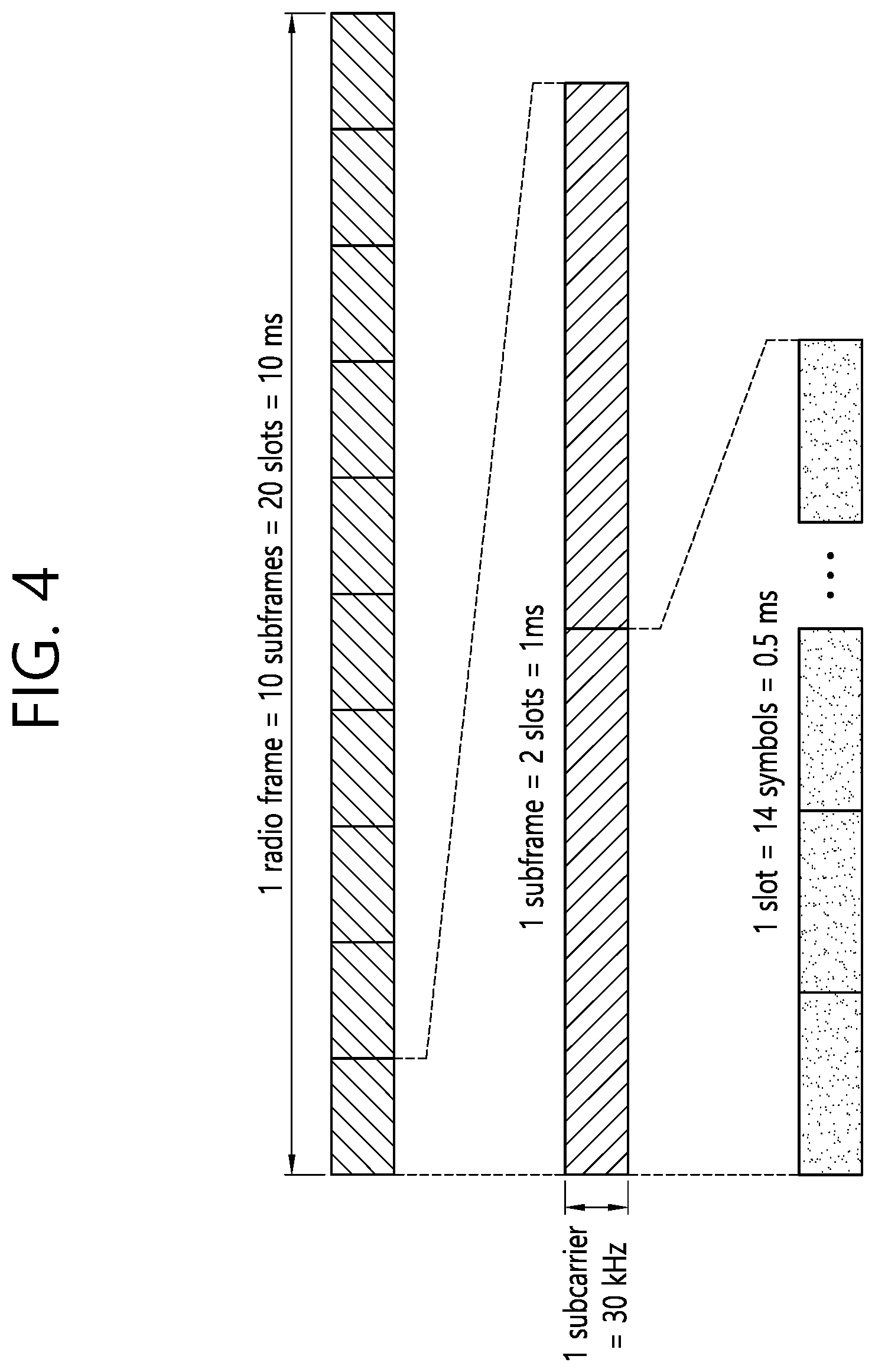
[0055] In the LTE standards (and the enhancements of the LTE standards), one radio frame includes 10 subframes, and one subframe includes two slots. The length of one subframe may be 1 ms, and the length of one slot may be 0.5 ms. The time during which one subframe is transmitted is referred to as a Transmission Time Interval (TTI). The TTI may be a minimum unit for scheduling.
[0056] Unlike the LTE standards, the NR standards support various numerologies, and therefore a variety of radio frame structures are established. The NR standards support a plurality of subcarrier spacings in the frequency domain, and NR numerologies are determined by the numerology being used. The following Table 1 tabulates multiple numerologies supported by NR. Each numerology is identified by the index ".mu.".
TABLE-US-00001 TABLE 1 Subcarrier Supported for Supported for .mu. spacing Cyclic prefix data synch 0 15 Normal Yes Yes 1 30 Normal Yes Yes 2 60 Normal, Yes No Extended 3 120 Normal Yes Yes 4 240 Normal No Yes
[0057] As shown in Table 1, the subcarrier spacing may be set to either 15, 30, 60, 120, or 240 kHz, and its specific numerical value may be varied. Thus, each spacing (e.g., .mu.=0, 1, . . . , 4) may be denoted by the first, second, . . . , Nth subcarrier spacings.
[0058] As shown in Table 1, some subcarrier spacings may not be used to send user data (for example, Physical Uplink Shared Channel (PUSCH), Physical Downlink Shared Channel (PDSCH), etc.). That is, user data transmission may not be supported for at least one preset subcarrier spacing (for example, 240 kHz).
[0059] Moreover, as shown in Table 1, synchronous channels (for example, Primary Synchronization Signal (PSS), Secondary Synchronization Signal (SSS), Physical Broadcast Channel (PBCH), etc.) may not be supported for some subcarrier spacings. That is, synchronous channels may be supported for at least one subcarrier spacing (e.g., 60 kHz).
[0060] In the NR standards, the number of slots and the number of symbols may be set differently depending on various numerologies, that is, various subcarrier spacings. A detailed example of this will be given in the following Table 2.
TABLE-US-00002 TABLE 2 Number of symbols Number of slots in a Number of slots in a .mu. in a slot radio frame subframe 0 14 10 1 1 14 20 2 2 14 40 4 3 14 80 8 4 14 160 16
[0061] According to Table 2, in the first numerology in which ".mu.=0", one radio frame includes 10 subframes, one subframe corresponds to 1 slot, and 1 slot includes 14 slots. In the present disclosure, the term `symbol` means a signal transmitted during a specific time period--for example, a signal generated by Orthogonal Frequency Division Multiplexing (OFDM) processing. That is, the term `symbol` used herein may refer to an OFDM/OFDMA symbol or an SC-FDMA symbol. A cyclic prefix (CP) may be positioned between each symbol.
[0062] FIG. 3 shows an example of application of a particular numerology. That is, FIG. 3 depicts a case in which .mu.=0. FIG. 4 shows an example of application of another numerology. That is, FIG. 4 depicts a case in which .mu.=1.
[0063] In the example in Table 2, a normal cyclic prefix (CP) may be applied. If an extended CP is applied, the numerology in the following Table 3 may be used.
TABLE-US-00003 TABLE 3 Number of symbols Number of slots in a Number of slots in a .mu. in a slot radio frame subframe 2 12 40 4
[0064] Meanwhile, Frequency Division Duplex (FDD) and/or Time Division Duplex (TDD) may be used in a wireless system in which an example of the present specification is applied. For TDD, in LTE systems, uplink and downlink subframes are allocated in subframes.
[0065] In NR standards/systems, each symbol may be distinguished by downlink (denoted by D), flexible (denoted by X), or uplink (denoted by U) as in the following table. The following table may be applied commonly to specific cells or adjacent cells or applied individually or differently to each UE.
TABLE-US-00004 TABLE 4 Symbol number in a slot Format 0 1 2 3 4 5 6 7 8 9 10 11 12 13 0 D D D D D D D D D D D D D D 1 U U U U U U U U U U U U U U 2 X X X X X X X X X X X X X X 3 D D D D D D D D D D D D D X 4 D D D D D D D D D D D D X X 5 D D D D D D D D D D D X X X 6 D D D D D D D D D D X X X X 7 D D D D D D D D D X X X X X 8 X X X X X X X X X X X X X U 9 X X X X X X X X X X X X U U 10 X U U U U U U U U U U U U U 11 X X U U U U U U U U U U U U 12 X X X U U U U U U U U U U U 13 X X X X U U U U U U U U U U 14 X X X X X U U U U U U U U U 15 X X X X X X U U U U U U U U 16 D X X X X X X X X X X X X X 17 D D X X X X X X X X X X X X 18 D D D X X X X X X X X X X X 19 D X X X X X X X X X X X X U 20 D D X X X X X X X X X X X U 21 D D D X X X X X X X X X X U 22 D X X X X X X X X X X X U U 23 D D X X X X X X X X X X U U
[0066] For convenience of explanation, Table 4 shows only some of the formats actually defined in the NR standards, and a specific allocation technique may be changed or added.
[0067] The UE may be assigned a slot format (i.e., TDD format) through an upper-layer signal, based on Downlink Control Information (DCI) sent via Physical Downlink Control Channel (PDCCH), or based on a combination of the upper-layer signal (i.e., RRC signal) and the DCI.
[0068] FIG. 5 is a view showing an example of a resource grid.
[0069] The example in FIG. 5 shows a time-frequency resource grid used in the NR standards. The example in FIG. 5 may be applied in uplink and/or downlink. As shown in the drawing, one subframe includes a plurality of slots on the time axis. Specifically, "142.mu." symbols may be represented within the resource grid based on the .mu. value. Also, as shown in the drawing, one resource block (RB) may occupy 12 contiguous subcarriers. One resource block may be referred to as a physical resource block (PRB), and each physical resource block may include 12 resource elements (RE). The number of resource blocks RB that can be allocated may be determined based on the smallest value and the largest value. Moreover, the number of resource blocks RB that can be allocated may be set individually according to the numerology ".mu.". It may have the same value or different values for uplink and downlink.
[0070] <Carrier Aggregation: CA>
[0071] Hereinafter, a carrier aggregation system will be described.
[0072] The carrier aggregation (CA) system means aggregating multiple component carriers (CCs). By the carrier aggregation, the existing meaning of the cell is changed. According to the carrier aggregation, the cell may mean a combination of a downlink component carrier and an uplink component carrier or a single downlink component carrier.
[0073] Further, in the carrier aggregation, the cell may be divided into a primary cell, secondary cell, and a serving cell. The primary cell means a cell that operates at a primary frequency and means a cell in which the UE performs an initial connection establishment procedure or a connection reestablishment procedure with the base station or a cell indicated by the primary cell during a handover procedure. The secondary cell means a cell that operates at a secondary frequency, and once an RRC connection is established, the secondary cell is configured and is used to provide an additional radio resource.
[0074] The carrier aggregation system may be divided into a continuous carrier aggregation system in which aggregated carriers are contiguous and a non-contiguous carrier aggregation system in which the aggregated carriers are separated from each other. Hereinafter, when the contiguous and non-contiguous carrier systems are just called a carrier aggregation system, it should be construed that the carrier aggregation system includes both a case in which the component carriers are contiguous and a case in which the component carriers are non-contiguous. The number of component carriers aggregated between the downlink and the uplink may be differently set. If the number of downlink CCs and the number of uplink CCs are the same, this is referred to as symmetric aggregation, and, if the number of downlink CCs and the number of uplink CCs are different, this is referred to as asymmetric aggregation.
[0075] Meanwhile, the carrier aggregation (CA) technologies, as described above, may be generally separated into an inter-band CA technology and an intra-band CA technology. The inter-band CA is a method that aggregates and uses CCs that are present in different bands from each other, and the intra-band CA is a method that aggregates and uses CCs in the same frequency band. Further, CA technologies are more specifically split into intra-band contiguous CA, intra-band non-contiguous CA, and inter-band non-contiguous CA.
[0076] FIGS. 6A and 6B are conceptual views illustrating Intra-Band Carrier aggregation (CA).
[0077] FIG. 6A illustrates intra-band contiguous CA, and FIG. 6B illustrates intra-band non-contiguous CA.
[0078] LTE-advanced has various schemes added to it, including uplink MIMO and carrier aggregation in order to realize high-speed wireless transmission. The CA that is being discussed in LTE-advanced may be split into the intra-band contiguous CA shown in FIG. 6A and the intra-band non-contiguous CA shown in FIG. 6B.
[0079] FIGS. 7A and 7B are conceptual views illustrating Inter-Band Carrier Aggregation.
[0080] FIG. 7A illustrates a combination of a lower band and a higher band for inter-band CA, and FIG. 7B illustrates a combination of similar frequency bands for inter-band CA.
[0081] In other words, the inter-band carrier aggregation may be separated into inter-band CA between carriers of a low band and a high band having different RF characteristics of inter-band CA as shown in FIG. 7A and inter-band CA of similar frequencies that may use a common RF terminal per component carrier due to similar RF (radio frequency) characteristics as shown in FIG. 7B.
[0082] <Operating Bands>
[0083] E-UTRRA may operate in the operating bands defined in Table 5 below.
TABLE-US-00005 TABLE 5 E-UTRA operating Uplink operating band Downlink operating band Duplex band F.sub.UL.sub.--.sub.low-F.sub.UL.sub.--.sub.high F.sub.DL.sub.--.sub.low-F.sub.DL.sub.--.sub.high mode 1 1920 MHz-1980 MHz 2110 MHz-2170 MHz FDD 2 1850 MHz-1910 MHz 1930 MHz-1990 MHz FDD 3 1710 MHz-1785 MHz 1805 MHz-1880 MHz FDD 4 1710 MHz-1755 MHz 2110 MHz-2155 MHz FDD 5 824 MHz-849 MHz 869 MHz-894MHz FDD 6 830 MHz-840 MHz 875 MHz-885 MHz FDD 7 2500 MHz-2570 MHz 2620 MHz-2690 MHz FDD 8 880 MHz-915 MHz 925 MHz-960 MHz FDD 9 1749.9 MHz-1784.9 MHz 1844.9 MHz-1879.9 MHz FDD 10 1710 MHz-1770 MHz 2110 MHz-2170 MHz FDD 11 1427.9 MHz-1447.9 MHz 1475.9 MHz-1495.9 MHz FDD 12 699 MHz-716 MHz 729 MHz-746 MHz FDD 13 777 MHz-787 MHz 746 MHz-756 MHz FDD 14 788 MHz-798 MHz 758 MHz-768 MHz FDD 15 Reserved Reserved FDD 16 Reserved Reserved FDD 17 704 MHz-716 MHz 734 MHz-746 MHz FDD 18 815 MHz-830 MHz 860 MHz-875 MHz FDD 19 830 MHz-845 MHz 875 MHz-890 MHz FDD 20 832 MHz-862 MHz 791 MHz-821 MHz FDD 21 1447.9 MHz-1462.9 MHz 1495.9 MHz-1510.9 MHz FDD 22 3410 MHz-3490 MHz 3510 MHz-3590 MHz FDD 23 2000 MHz-2020 MHz 2180 MHz-2200 MHz FDD 24 1626.5 MHz-1660.5 MHz 1525 MHz-1559 MHz FDD 25 1850 MHz-1915 MHz 1930 MHz-1995 MHz FDD 26 814 MHz-849 MHz 859 MHz-894 MHz FDD 27 807 MHz-824 MHz 852 MHz-869 MHz FDD 28 703 MHz-748 MHz 758 MHz-803 MHz FDD 29 N/A 717 MHz-728 MHz FDD 30 2305 MHz-2315 MHz 2350 MHz-2360 MHz FDD 31 452.5 MHz-457.5 MHz 462.5 MHz-467.5 MHz FDD 32 N/A 1452 MHz-1496 MHz FDD . . . 33 1900 MHz-1920 MHz 1900 MHz-1920 MHz TDD 34 2010 MHz-2025 MHz 2010 MHz-2025 MHz TDD 35 1850 MHz-1910 MHz 1850 MHz-1910 MHz TDD 36 1930 MHz-1990 MHz 1930 MHz-1990 MHz TDD 37 1910 MHz-1930 MHz 1910 MHz-1930 MHz TDD 38 2570 MHz-2620 MHz 2570 MHz-2620 MHz TDD 39 1880 MHz-1920 MHz 1880 MHz-1920 MHz TDD 40 2300 MHz-2400 MHz 2300 MHz-2400 MHz TDD 41 2496 MHz-2690 MHz 2496 MHz-2690 MHz TDD 42 3400 MHz-3600 MHz 3400 MHz-3600 MHz TDD 43 3600 MHz-3800 MHz 3600 MHz-3800 MHz TDD 44 703 MHz-803 MHz 703 MHz-803 MHz TDD
[0084] NR may operate in the FR1 operating bands defined in Table 6 below.
TABLE-US-00006 TABLE 6 NR operating Uplink operating band Downlink operating band Duplex band F.sub.UL.sub.--.sub.low-F.sub.UL.sub.--.sub.high F.sub.DL.sub.--.sub.low-F.sub.DL.sub.--.sub.high mode n1 1920 MHz-1980 MHz 2110 MHz-2170 MHz FDD n2 1850 MHz-1910 MHz 1930 MHz-1990 MHz FDD n3 1710 MHz-1785 MHz 1805 MHz-1880 MHz FDD n5 824 MHz-849 MHz 869 MHz-894 MHz FDD n7 2500 MHz-2570 MHz 2620 MHz-2690 MHz FDD n8 880 MHz-915 MHz 925 MHz-960 MHz FDD n20 832 MHz-862 MHz 791 MHz-821 MHz FDD n28 703 MHz-748 MHz 758 MHz-803 MHz FDD n38 2570 MHz-2620 MHz 2570 MHz-2620 MHz TDD n41 2496 MHz-2690 MHz 2496 MHz-2690 MHz TDD n50 1432 MHz-1517 MHz 1432 MHz-1517 MHz TDD n51 1427 MHz-1432 MHz 1427 MHz-1432 MHz TDD n66 1710 MHz-1780 MHz 2110 MHz-2200 MHz FDD n70 1695 MHz-1710 MHz 1995 MHz-2020 MHz FDD n71 663 MHz-698 MHz 617 MHz-652 MHz FDD n74 1427 MHz-1470 MHz 1475 MHz-1518 MHz FDD n75 N/A 1432 MHz-1517 MHz SDL n76 N/A 1427 MHz-1432 MHz SDL n77 3300 MHz-4200 MHz 3300 MHz-4200 MHz TDD n78 3300 MHz-3800 MHz 3300 MHz-3800 MHz TDD n79 4400 MHz-5000 MHz 4400 MHz-5000 MHz TDD n80 1710 MHz-1785 MHz N/A SUL n81 880 MHz-915 MHz N/A SUL n82 832 MHz-862 MHz N/A SUL n83 703 MHz-748 MHz N/A SUL n84 1920 MHz-1980 MHz N/A SUL n86 1710 MHz-1780 MHz N/A SUL
[0085] NR may operate in the FR2 operating bands defined in Table 7 below.
TABLE-US-00007 TABLE 7 NR operating Uplink operating band Downlink operating band Duplex band F.sub.UL.sub.--.sub.low-F.sub.UL.sub.--.sub.high F.sub.DL.sub.--.sub.low-F.sub.DL.sub.--.sub.high mode n257 26500 MHz-29500 MHz 26500 MHz-29500 MHz TDD n258 24250 MHz-27500 MHz 24250 MHz-27500 MHz TDD n260 37000 MHz-40000 MHz 37000 MHz-40000 MHz TDD n261 27500 MHz-28350 MHz 27500 MHz-28350 MHz TDD
[0086] When the operating bands are defined as shown in Table 5, Table 6, and Table 7, each nation's frequency distributing organization may assign specific frequencies to service providers in compliance with the nation's circumstances.
[0087] FIG. 8 illustrates an example of operating bands used in each continent.
[0088] As can be seen with reference to FIG. 8, in Europe, bands 1, 3, 7, 8, 20 and 28, among the E-UTRA operating bands according to Table 5, and bands n78 and n258, among the NR operating bands according to Table 6 and FIG. 7, may be used. In Asia, bands 1, 3, 5, 7, 8, 18, 19, 21, 28, 39, 41, and 42, among the E-UTRA operating bands according to Table 5, and bands n41, n77, n78, n79, and n258, among the NR operating bands according to Table 6 and Table 7, may be used. In North America, bands 2, 4, 5, 12, 13, 41, 65, and 71, among the E-UTRA operating bands according to Table 5, and bands n257, n260, and n261, among the NR operating bands according to Table 6 and Table 7, may be used.
[0089] Details of the used frequency bands illustrated in FIG. 8 are summarized in Table 8 below.
TABLE-US-00008 TABLE 8 Europe Asia North America E-UTRA 1 .largecircle. .largecircle. operating 2 .largecircle. band 3 .largecircle. .largecircle. 4 .largecircle. 5 .largecircle. .largecircle. 7 .largecircle. .largecircle. 8 .largecircle. .largecircle. 12 .largecircle. 13 .largecircle. 18 .largecircle. 19 .largecircle. 20 .largecircle. 21 .largecircle. 28 .largecircle. .largecircle. 39 .largecircle. 41 .largecircle. .largecircle. 42 .largecircle. 65 .largecircle. 71 .largecircle. NR n28 .largecircle. operating n77 .largecircle. band n78 .largecircle. .largecircle. n79 .largecircle. n257 .largecircle. n258 .largecircle. .largecircle. n260 .largecircle. n261 .largecircle.
[0090] Referring to FIG. 8 and Table 8, different frequency bands are used in each continent (region). In some cases, some frequency bands may be commonly used in each continent. For example, the E-UTRA operating bands 1, 3, 7, and 8 are frequency bands commonly used in Europe and Asia, and E-UTRA operating bands 5 and 41 are frequency bands commonly used in Asia and North America.
[0091] Meanwhile, the frequency bands used in each continent (region) are not limited to FIG. 8 and Table 8. That is, even a frequency band not shown in FIG. 8 and Table 8 also may be used in each continent (region).
[0092] Meanwhile, in the current 5G NR technology, a scheme (EN-DC) of dually connecting LTE and NR is underway to ensure communication stability. However, in a state in which a downlink carrier using LTE and a downlink carrier using NR are aggregated, transmission of an uplink signal may cause a harmonic component and an intermodulation distortion (IMD) component to affect a downlink band of the UE itself.
[0093] Specifically, the UE must be set to satisfy a reference sensitivity power level (REFSENS), which is minimum average power for each antenna port of the UE. However, in a case where the harmonic component and/or IMD component are generated, the REFSENS for the downlink signal may not be satisfied. That is, the REFSENS must be set such that throughput thereof is at least 95% of maximum throughput of a reference measurement channel, but the generation of the harmonic component and/or IMD component may cause the throughput to fall below 95%.
[0094] Thus, it is determined whether a harmonic component and/or IMD component have been generated in the EN-DC terminal (or EN-DC user equipment (UE)) or not, and, when it is determined that the harmonic component and IMD component have been generated, a maximum sensitivity degradation (MSD) value for a corresponding frequency band may be defined to allow relaxation for the REFSENS in a reception band of the EN-DC terminal based on a transmission signal of the EN-DC terminal. Here, the MSD is maximum allowable degradation of REFSENS, and in a certain frequency band, the REFSENS may be relaxed by the defined amount of MSD.
[0095] FIG. 9 illustrates that, when an uplink signal is transmitted through an uplink carrier, a harmonic component and an intermodulation distortion (IMD) component enter downlink bands of the UE.
[0096] Referring to FIG. 9, in a case where three downlink bands are established by carrier aggregation and two uplink bands are established, when the UE transmits an uplink signal through two uplink bands, the harmonic component and the IMD component may enter downlink bands of the UE.
[0097] In this situation, an MSD value capable of correcting the REFSENS is proposed to prevent reception sensitivity of a downlink signal from deteriorating due to the harmonic component and/or IMD component.
[0098] In addition, although the UE appropriately solves the problem, a degradation of a reception sensitivity level in the downlink band of the UE may not be completely prevented due to cross isolation and coupling loss due to the PCB, a scheme for relaxing the existing requirements that the UE must meet is proposed.
[0099] <Disclosure of the Present Disclosure>
[0100] Hereinafter, in a case where the UE transmits an uplink signal through two uplink carriers when multiple downlink carriers and multiple plink carriers are aggregated, any leakage of interference to a downlink band of the UE is analyzed and a solution thereto is subsequently proposed.
[0101] I. Analysis of Harmonics
[0102] Hereinafter, the harmonics of an EN_DC_20A_28A-n75A band combination will be analyzed.
[0103] Table 9 shows the operating bands and duplex modes in EN_DC_20A_28A-n75A.
TABLE-US-00009 TABLE 9 Downlink operating Uplink operating band band EN-DC BS reception/UE BS transmission/UE operating E-UTRA and transmission reception Duplex band NR bands F.sub.UL.sub.--.sub.low-F.sub.UL.sub.--.sub.high F.sub.DL.sub.--.sub.low-F.sub.DL.sub.--.sub.high mode DC_20A_n28A-n75A 20 832 MHz-862 MHz 791 MHz-821 MHz FDD n28 703 MHz-733 MHz 758 MHz-788 MHz n75 N/A 1432 MHz-1517 MHz SDL
[0104] In Table 9, the E-UTRA operating band 20 may be defined from uplink 703 to 748 MHz and downlink 758 to 803 MHz. Also, the second harmonic of the NR operating band n28 may affect the reception of the NR operating band n75. Accordingly, a harmonic filter for EN_DC_20A_28A-n75A may be taken into consideration in order to reduce the harmonic problem with reception in the NR operating band n75.
[0105] Table 10 shows common isolation parameters for RF FE components of EN_DC_20A_28A-n75A UE.
TABLE-US-00010 TABLE 10 Attenuation Value B28 Tx in PA output 28 B28 PA H2 attenuation 35 B28 duplexer H2 attenuation 33 Harmonic filter 20 LB switch H2 120 Diplexer attenuation 25 Antenna isolation 0 Diplexer pathloss 0.7 MB switch attenuation 0.7 MB switch 130/110 (primary/secondary) nB75 Rx filter attenuation 1.5 nB75 Rx filter 110/110 (primary/secondary) B28 PA to n75 LNA isolation 60
[0106] Table 11 shows common parameters for the analysis of MDM for EN-DC_20A_n28A-n75A.
TABLE-US-00011 TABLE 11 When a harmonic trap filter is considered Primary Diversity Parameter Value H8 level Value H8 level B28 Tx in PA output 28 28 B28 PA H2 attenuation 35 -7 35 -7 B28 duplexer H2 attenuation 33 -40 33 -40 Harmonic filter 20 -60 20 -60 LB switch H2 -120 -60.0 -120 -60.0 Diplexer attenuation 25 -85.0 25 -85.0 Antenna isolation 0 -85.0 10 -95.0 Diplexer pathloss 0.7 -85.7 0.7 -95.7 MB switch attenuation 0.7 -86.4 0.7 -96.4 MB switch -130 -86.4 -110 -96.2 nB75 Rx filter attenuation 1.5 -87.9 1.5 -97.7 nB75 Rx filter -110 -87.9 -110 -97.5 B28 PA to n75 LNA isolation 60 -67.0 60 -67.0 Composite -66.96 -66.99 After MRC 28.1 dB
[0107] The second harmonic which affects transmission in the NR operating band n28 needs to be analyzed, in order to use the EN_DC_20A_n28A-n75A band combination.
[0108] Accordingly, Table 12 shows the MSD value for CA_n28A-n75A when the common parameters shown in Table 11 are taken into consideration.
TABLE-US-00012 TABLE 12 MSD value for second harmonic of NR n75 reception operating band 5 MHz 10 MHz 15 MHz 20 MHz UL band DL band dB dB dB dB n28 n75 28.1 25.3 24.0 22.8
[0109] Moreover, additional ILs for each vendor caused by the harmonic trap filter are proposed as in Table 13.
TABLE-US-00013 TABLE 13 Attenuation IL for UL operating IL for DL operating value (dB) for band of NR n28 band of NR n28 n75 Vendor A 0.5 0.52 20 Vendor B 0.53 0.47 23 Vendor C 0.44 0.42 22 Average 0.49 0.47 22
[0110] According to the shared pain access method in LTE CA, additional ILs for NR_n28A-n75A UE are proposed as in Table 14b.
TABLE-US-00014 TABLE 14 Operating band .DELTA.T.sub.IB, c [dB] in n28 .DELTA.R.sub.IB, c [dB] in n28 NR-CA_n28A-n75A 0.2 0.2
[0111] The additional ILs proposed in Table 14 may apply in the NR operating band n28 in NR CA n28A-n75A.
[0112] Table 15 and Table 16 show .DELTA.T.sub.IB,c and .DELTA.R.sub.IB proposed for the actual EN-DC band combination EN-DC_20A_n28A-n75A.
TABLE-US-00015 TABLE 15 Inter-band DC configuration E-UTRA and NR bands .DELTA.T.sub.IB, c [dB] DC_20A_n28A-n75A 20 0.5 n28 0.7
TABLE-US-00016 TABLE 16 Inter-band DC configuration E-UTRA and NR bands .DELTA.R.sub.IB, c [dB] DC_20A_n28A-n75A 20 0.0 n28 0.2 n75 0.0
[0113] That is, the T.sub.ib of the NR operating band n28 in the EN-DC_20A_n28A UE may be as shown in Table 15 due to an increase from 0.5 dB by 0.2 dB, and the R.sub.ib of the NR operating band n28 in the EN-DC_20A_n28A UE may be as shown in Table 16 due to an increase from 0.0 dB by 0.2 dB.
[0114] II. MSD Proposal
[0115] Hereinafter, MSD values are proposed to support EN-DC operation even when self-interference affects the UE's own Rx frequency bands regardless of Pcell and Scell.
[0116] In an LTE system, a shared antenna RF architecture for non-standalone (NSA) terminals of 6 GHz or lower may be considered. Thus, a shared antenna RF architecture for generic NSA DC UE may be considered to derive MSD values.
[0117] However, a separate RF architecture needs to be taken into consideration in the case of some DC band combinations, such as DC_42A-n77A, DC_42A-n78A, and DC_41_n41A, where the operating frequency ranges of the NR band and the LTE band overlap.
[0118] Accordingly, for the analysis of MSD for 3DL/2UL DC UE such as DC_42A-n77A, DC_42A-n78A, and DC_41_n41A, parameters and attenuation levels are assumed based on the UE RF FE components shown in Table 17 and Table 18.
[0119] Table 17 shows RF component isolation parameters for deriving MSD values at 6 GHz or lower.
TABLE-US-00017 TABLE 17 UE ref. architecture Triplexer-Diplexer Architecture w/single ant. DC_1A-41A_n77A, DC_1A-41A_n79A, DC_1A-42A_n79A, DC_1A-18A_n79A, DC_1A-28A_n79A, DC_3A-28A_n77A, DC_3A-28A_n79A, DC_21A-28A_n77A, Cascaded-Diplexer architecture w/single ant. DC_21A-28A_n79A, DC_28A-42A_n79A DC_1A-7A_n78A IP2 IP3 IP4 IP5 IP2 IP3 IP4 IP5 Component (dBm) (dBm) (dBm) (dBm) (dBm) (dBm) (dBm) (dBm) Ant. Switch 112 68 55 55 112 68 55 55 Triplexer 110 72 55 52 Diplexer 115 87 55 55 115 87 55 55 Duplexer 100 75 55 53 100 75 55 53 PA Forward 28.0 32 30 28 28.0 32 30 28 PA Reversed 40 30.5 30 30 40 30.5 30 30 LNA 10 0 0 -10 10 0 0 -10
[0120] Table 18 shows isolation levels for different RF components.
TABLE-US-00018 TABLE 18 Isolation Parameter Value (dB) Comment Antenna to Antenna 10 Main antenna to diversity antenna PA (out) to PA (in) 60 PCB isolation (PA forward mixing) Triplexer 20 High/low band isolation Quadplexer 15 L-L or H-M band isolation Diplexer 25 High/low band isolation PA (out) to PA (out) 60 L-H/H-L cross-band PA (out) to PA (out) 50 H-H cross-band LNA (in) to PA (out) 60 L-H/H-L cross-band LNA (in) to PA (out) 50 H-H cross-band Duplexer 50 Tx band rejection at Rx band
[0121] Table 19 shows MSD values proposed according to Table 17 and Table 18.
TABLE-US-00019 TABLE 19 UL UL Fc UL BW UL DL Fc DL BW CF MSD DC bands DC IMD (MHz) (MHz) RB# (MHz) (MHz) (dB) (dB) DC_1A-41A_n77A 1 IMD4 |3*fB1 - fn77| 1970 5 25 2160 5 0.7 N/A n77 3400 10 52 3400 10 41 2510 5 25 2510 5 9.9 1 IMD5 |3*fB1 - 2*fn77| 1930 5 25 2120 5 0.4 N/A n77 4150 10 52 4150 10 41 2510 5 25 2510 5 4.0 DC_1A-41A_n79A 1 IMD2 |fB1 - fn79| 1970 5 25 2160 5 2.2 N/A n79 4500 40 216 4500 40 41 2530 5 25 2530 5 29.4 1 IMD5 |4*fB1 - fn79| 1922.5 5 25 2112.5 5 0 N/A n79 4980 40 216 4980 40 41 2687.5 5 25 2687.5 5 0.0 DC_1A-42A_n79A 1 IMD5 |4*fB1 - fn79| 1977.5 5 25 2167.5 5 0.6 N/A n79 4420 40 216 4420 40 42 3490 5 25 3490 5 4.8 42 IMD3 |2*fB42 - fn79| 3402.5 5 25 3402.5 5 1.6 N/A n79 4640 40 216 4640 40 1 1975 5 25 2165 5 15.5 42 IMD4 |2*fB42 - 2*fn79| 3450 5 25 3450 5 0.9 N/A n79 4520 40 216 4520 40 1 1950 5 25 2140 5 9.3 DC_1A-18A_n79A 1 IMD4 |3*fB1 - fn79| 1930 5 25 2120 5 0.8 N/A n79 4925 40 216 4925 40 18 820 5 25 865 5 8.9 DC_1A-28A_n79A 1 IMD3 |2*fB1 - fn79| 1930 5 25 2120 5 1.3 N/A n79 4648 40 216 4648 40 28 733 5 25 788 5 15.2 1 IMD4 |2*fB1 - 2*fn79| 1925 5 25 2115 5 0.9 N/A n79 4980 40 216 4980 40 28 740 5 25 795 5 10.0 28 IMD4 |3*fB28 - fn79| 745.5 5 25 800.5 5 0 N/A n79 4420 40 216 4420 40 1 1977.5 5 25 2167.5 5 1.2 28 IMD5 |4*fB28 - fn79| 718 5 25 773 5 0.4 N/A n79 4807 40 216 4807 40 1 1935 5 25 2125 5 4.5 DC_1A-7A_n28A 1 IMD2 |fB1 + fn28| 1935 5 25 2125 5 2.0 N/A n28 718 5 25 773 5 7 2533 10 52 2653 10 28.8 DC_3A-28A_n77A 3 IMD3 |2*fB3 - fn77| 1712.5 5 25 1807.5 5 1.6 N/A n77 4195 10 52 4195 10 28 715 5 25 770 5 16.2 28 IMD3 |2*fB28 - fn77| 735 5 25 790 5 1.6 N/A n77 3320 10 52 3320 10 3 1755 5 25 1850 5 16.7 DC_3A-28A_n79A 3 IMD4 |3*fB3 - fn79| 1770 5 25 1865 5 0.8 N/A n79 4530 40 216 4530 40 28 725 5 25 780 5 10.3 28 IMD5 |4*fB28 - fn79| 725 5 25 780 5 0.5 N/A n79 4770 40 216 4770 40 3 1775 5 25 1870 5 5.7 DC_21A-28A_n77A 21 IMD3 |2*fB21 - fn77| 1452 5 25 1500 5 1.6 N/A n77 3689.5 10 52 3689.5 10 28 730.5 5 25 785.5 5 15.8 28 IMD4 |3*fB28 - fn77| 730.5 5 25 785.5 5 1.0 N/A n77 3690 10 52 3690 10 21 1450.5 5 25 1498.5 5 11.0 DC_21A-28A_n79A 28 IMD5 |4*fB28 - fn79| 730.5 5 25 785.5 5 0.5 N/A n79 4420 40 216 4420 40 21 1450 5 25 1498 5 5.2 DC_28A-42A_n79A 28 IMD3 |2*fB28 - fn79| 730 5 25 785 5 1.5 N/A n79 4880 40 216 4880 40 42 3420 5 25 3420 5 15.3 42 IMD2 |fB42 - fn79| 3597.5 5 25 3597.5 5 0.0 N/A n79 4420 40 216 4420 40 28 745 5 25 800 5 16.2
[0122] In some embodiments, the MSD values proposed in Table 19 may allow a margin of error of .+-.1 dB.
[0123] Table 20 shows MSD values for DC_1A-18A-n79A in addition to those in Table 19.
TABLE-US-00020 TABLE 20 E-UTRA and NR Band/Channel bandwidth/NRB/Duplex mode EUTRA UL/DL DC and NR UL Fc BW UL DL Fc MSD Duplex Source Configuration band (MHz) (MHz) CLRB (MHz) (dB) mode of IMD DC_1A-18A-n79A 1 1935 5 25 2125 N/A FDD N/A 18 822.5 5 25 867.5 18.3 IMD3 n79 4782.5 40 216 4782.5 N/A TDD N/A 1 1930 5 25 2120 N/A FDD N/A 18 820 5 25 865 8.9 IMD4 n79 4925 40 216 4925 N/A TDD N/A 1 1935 5 25 2125 8.1 FDD IMD4 18 822.5 5 25 867.5 N/A N/A n79 4782.5 40 216 4782.5 N/A TDD N/A
[0124] FIG. 10 is a flowchart according to a disclosure of the present specification, and FIG. 11 illustrates an example according to a disclosure of the present specification.
[0125] Referring to FIG. 10, a UE supporting dual-connectivity between E-UTRA and NR may preset a maximum sensitivity degradation (MSD) regarding reference sensitivity (REFSENS) to apply the same to reception of a downlink signal (S1010). When receiving a downlink signal, the UE may receive the downlink signal by applying the preset MSD value (S1020).
[0126] As described above with reference to FIG. 9, in the case of a UE supporting dual-connectivity between E-UTRA and NR, when the UE transmits an uplink signal through two uplink bands, a harmonic component (harmonics) and/or an intermodulation distortion (IMD) component generated according to a frequency band of the uplink signal may enter a downlink band of the UE. Here, in order to prevent a degradation of reception sensitivity of the downlink signal due to the harmonic component and/or IMD component, the UE may apply maximum sensitivity degradation (MSD) correcting the REFSENS.
[0127] Here, the preset MSD may be an MSD value described in Table 19 and Table 20. That is, when the conditions described in Table 19 and Table 20 are applied, the UE may receive the downlink signal by applying the proposed MSD value.
[0128] For example, referring to FIG. 11 and Table 19, when the UE supports dual-connectivity between the E-UTRA operating bands 1 and 41 and the NR operating band n79, if an uplink center frequency and downlink center frequency of the E-UTRA operating band 41 are 2530 MHz, the second IMD (IMD2) may enter the downlink operating band. Thus, in order to prevent a degradation of reception sensitivity of the downlink signal due to the second IMD component IMD2, the MSD value may be set to 29.4 dB to correct reference sensitivity.
[0129] Moreover, FIG. 10 also may apply to a UE supporting NR CA. That is, a UE supporting NR CA may preset a maximum sensitivity degradation (MSD) regarding reference sensitivity (REFSENS) to apply the same to reception of a downlink signal (S1010). When receiving a downlink signal, the UE may receive the downlink signal by applying the preset MSD value (S1020).
[0130] Here, the preset MSD may be an MSD value described in Table 12. That is, when the conditions described in Table 12 are applied, the UE may receive the downlink signal by applying the proposed MSD value.
[0131] For example, referring to Table 12, when the UE supports CA of the NR operating bands n28 and n75, if SCS is 5 MHz, the second IMD (IMD2) may enter the downlink operating band of the NR operating band n75. Thus, in order to prevent a degradation of reception sensitivity of the downlink signal due to the second IMD component IMD2, the MSD value may be set to 28.1 dB to correct reference sensitivity.
[0132] FIG. 12 is a block diagram illustrating a wireless communication system according to one embodiment of a disclosure of the present specification.
[0133] Referring to FIG. 12, the wireless communication system may comprise at least one user equipment (UE) 100 and a base station 200.
[0134] The UE 100 may comprise a transceiver 110, a processor 120, and a memory 130. The memory 130 may be connected to the processor 120 to store various information for driving the processor 120. The transceiver 110 may be connected to the processor 120 to transmit and/or receive radio signals. The processor 120 may implement the proposed functions, processes, and/or methods.
[0135] The UE 100 may support dual-connectivity between E-UTRA and NR. When the UE 100 is configured to aggregate at least two carriers, the processor 120 may control the transceiver 110 to transmit the uplink signal using the uplink of the at least two carriers and receive the downlink signal using the downlink of the at least two carriers.
[0136] If the at least two carriers include at least one of the E-UTRA operating bands 1, 3, 5, 7, 18, 21, 28, 41, and 42 and one of the NR operating bands n28, n77, and n79, the processor 120 may receive the downlink signal by applying a preset MSD according to Table 19 and Table 20.
[0137] That is, in the case of the UE 100 supporting dual-connectivity between E-UTRA and NR, when the UE 100 transmits an uplink signal through two uplink bands, the harmonic component and/or IMD component generated according to a frequency band of the uplink signal may enter a downlink band of the UE 100, and thus, in order to prevent a degradation of reception sensitivity of the downlink signal due to the harmonic component and/or IMD component, the UE 100 may receive downlink signal by applying the MSD to correct the REFSENS.
[0138] The UE 100 may support NR CA. When the UE 100 is configured to aggregate the NR operating bands n28 and n79, the processor 120 may receive the downlink signal of the NR operating band n79 by applying a preset MSD according to Table 19 and Table 20.
[0139] The base station 200 may comprise a transceiver 210, a processor 220, and a memory 230. The memory 230 may be connected to the processor 220 to store various information for driving the processor 220. The transceiver 210 may be connected to the processor 220 to transmit and/or receive radio signals. The processor 220 may implement the proposed functions, processes, and/or methods.
[0140] The base station 200 may receive an uplink signal from the UE 100 using the transceiver 210 and transmit a downlink signal to the UE 100 using the transceiver 210. When the base station 200 transmits the downlink signal, the UE 100 may receive the downlink signal by using a preset MSD value according to Table 12, Table 19, and Table 20.
[0141] The processor may include Application-Specific Integrated Circuits (ASICs), other chipsets, logic circuits, and/or data processors. The memory may include Read-Only Memory (ROM), Random Access Memory (RAM), flash memory, memory cards, storage media and/or other storage devices. The RF unit may include a baseband circuit for processing a radio signal. When an embodiment is implemented in software, the above-described scheme may be implemented using a module (process or function) which performs the above function. The module may be stored in the memory and executed by the processor. The memory may be disposed to the processor internally or externally and connected to the processor using a variety of well-known means.
[0142] The embodiments of the present disclosure which has been described up to now may be implemented through various means. For example, the embodiments of the present disclosure may be implemented by hardware, firmware, software, or combinations thereof. In detail, the embodiments will be descried with reference to the drawings.
[0143] FIG. 13 is a detailed block diagram of the transceiver of the wireless device illustrated in FIG. 12.
[0144] Referring to FIG. 13, the transceiver 110 includes a transmitter 111 and a receiver 112. The transmitter 111 includes a discrete Fourier transform (DFT) unit 1111, a subcarrier mapper 1112, an IFFT unit 1113, a CP inserting unit 1144, and a wireless transmitter 1115. The transmitter 111 may further include a modulator. The transceiver 110 may further include a scramble unit, a modulation mapper (not shown), a layer mapper, and a layer permutator, which may be arranged before the DFT unit 1111. That is, in order to prevent an increase in peak-to-average power ratio (PAPR), the transmitter 111 first passes information through the DFT 1111 before mapping a signal to a subcarrier. A signal spread (or precoded in the same sense) by the DFT unit 1111 is subcarrier-mapped through the subcarrier mapper 1112 and then made to a signal on a time axis through the inverse fast Fourier transform (IFFT) unit 1113.
[0145] The DFT unit 1111 performs DFT on the input symbols to output complex-valued symbols. For example, when Ntx symbols are input (however, Ntx is a natural number), the DFT size is Ntx. The DFT unit 1111 may be referred to as a transform precoder. The subcarrier mapper 1112 maps the complex-valued symbols to subcarriers in the frequency domain. The complex-valued symbols may be mapped to resource elements corresponding to resource blocks allocated for data transmission. The subcarrier mapper 1112 may be referred to as a resource element mapper. The IFFT unit 1113 performs IFFT on the input symbol and outputs a baseband signal for data, which is a time domain signal. The CP inserting unit 1114 copies a part of the rear part of the base band signal for data and inserts the copied rear part to the front part of the base band signal for data. Inter-symbol interference (ISI) and inter-carrier interference (ICI) are prevented through CP insertion, and orthogonality may be maintained in a multi-path channel.
[0146] On the other hand, the receiver 112 includes a wireless receiving unit 1121, a CP removing unit 1122, an FFT unit 1123, and an equalizing unit 1124. The wireless receiving unit 1121, the CP removing unit 1122 and the FFT unit 1123 of the receiver 112 perform a reverse function of the wireless receiving unit 1115, the CP removing unit 1114 and the FFT unit 1113 of the transmitter 111. The receiver 112 may further include a demodulator.
* * * * *
D00000
D00001
D00002
D00003
D00004
D00005
D00006
D00007
D00008
D00009
D00010
D00011
D00012

D00013

D00014

D00015

XML
uspto.report is an independent third-party trademark research tool that is not affiliated, endorsed, or sponsored by the United States Patent and Trademark Office (USPTO) or any other governmental organization. The information provided by uspto.report is based on publicly available data at the time of writing and is intended for informational purposes only.
While we strive to provide accurate and up-to-date information, we do not guarantee the accuracy, completeness, reliability, or suitability of the information displayed on this site. The use of this site is at your own risk. Any reliance you place on such information is therefore strictly at your own risk.
All official trademark data, including owner information, should be verified by visiting the official USPTO website at www.uspto.gov. This site is not intended to replace professional legal advice and should not be used as a substitute for consulting with a legal professional who is knowledgeable about trademark law.