Display Devices And Manufacturing Method Thereof
KIM; Kwang Nyun ; et al.
U.S. patent application number 16/871128 was filed with the patent office on 2021-01-28 for display devices and manufacturing method thereof. The applicant listed for this patent is Samsung Display Co., Ltd.. Invention is credited to Ki Chul BAE, Chul Kyu CHOI, In HUH, Jong Hak HWANG, Kwang Nyun KIM, Chang Yong LEE, Seung Min LEE, Jong Gil RYU.
| Application Number | 20210028362 16/871128 |
| Document ID | / |
| Family ID | 1000004859618 |
| Filed Date | 2021-01-28 |


View All Diagrams
| United States Patent Application | 20210028362 |
| Kind Code | A1 |
| KIM; Kwang Nyun ; et al. | January 28, 2021 |
DISPLAY DEVICES AND MANUFACTURING METHOD THEREOF
Abstract
An embodiment of the present inventive concept provides a display device including: a mother substrate on which a plurality of display modules are located; and a mother film located on a rear surface of the mother substrate, wherein the mother film may include a first layer, and a second layer disposed between the first layer and the mother substrate, the second layer has a thickness of from about 40 .mu.m to about 60 .mu.m, and a thickness of the first layer may be greater than that of the second layer.
| Inventors: | KIM; Kwang Nyun; (Cheonan-si, KR) ; BAE; Ki Chul; (Asan-si, KR) ; RYU; Jong Gil; (Gwangmyeong-si, KR) ; LEE; Seung Min; (Hwaseong-si, KR) ; LEE; Chang Yong; (Cheonan-si, KR) ; CHOI; Chul Kyu; (Asan-si, KR) ; HUH; In; (Seongnam-si, KR) ; HWANG; Jong Hak; (Yongin-si, KR) | ||||||||||
| Applicant: |
|
||||||||||
|---|---|---|---|---|---|---|---|---|---|---|---|
| Family ID: | 1000004859618 | ||||||||||
| Appl. No.: | 16/871128 | ||||||||||
| Filed: | May 11, 2020 |
| Current U.S. Class: | 1/1 |
| Current CPC Class: | B32B 2367/00 20130101; H01L 27/3223 20130101; H01L 51/56 20130101; B32B 2457/20 20130101; B32B 7/12 20130101; B32B 37/02 20130101; B32B 27/281 20130101; H01L 51/0097 20130101; H01L 2251/566 20130101; H01L 27/3244 20130101; H01L 51/003 20130101; B32B 38/0004 20130101; B32B 37/12 20130101; B32B 27/36 20130101; B32B 27/08 20130101; H01L 2227/326 20130101; B32B 43/006 20130101; H01L 2251/5338 20130101; B32B 2379/08 20130101 |
| International Class: | H01L 51/00 20060101 H01L051/00; H01L 27/32 20060101 H01L027/32; H01L 51/56 20060101 H01L051/56; B32B 7/12 20060101 B32B007/12; B32B 27/36 20060101 B32B027/36; B32B 27/08 20060101 B32B027/08; B32B 37/02 20060101 B32B037/02; B32B 38/00 20060101 B32B038/00; B32B 43/00 20060101 B32B043/00; B32B 27/28 20060101 B32B027/28; B32B 37/12 20060101 B32B037/12 |
Foreign Application Data
| Date | Code | Application Number |
|---|---|---|
| Jul 22, 2019 | KR | 10-2019-0088330 |
Claims
1. A display device comprising: a mother substrate on which a plurality of display modules are located; and a mother film located on a rear surface of the mother substrate, wherein the mother film includes a first layer and a second layer disposed between the first layer and the mother substrate, the second layer has a thickness of from about 40 .mu.m to about 60 .mu.m, and a thickness of the first layer is greater than that of the second layer.
2. The display device of claim 1, wherein the second layer includes a pressure sensitive adhesive.
3. The display device of claim 1, wherein the first layer includes polyethylene terephthalate (PET).
4. The display device of claim 3, wherein the first layer has a thickness of from about 60 .mu.m to about 90 .mu.m.
5. The display device of claim 1, wherein the substrate is a flexible substrate including polyimide.
6. A manufacturing method of a display device, comprising: preparing a substrate including a plurality of display modules; and attaching a mother film to a rear surface of the substrate, wherein the mother film includes a first layer and a second layer disposed between the first layer and the mother substrate, and the second layer has a thickness of from about 40 .mu.m to about 60 .mu.m.
7. The manufacturing method of the display device of claim 6, wherein the second layer includes a pressure sensitive adhesive.
8. The manufacturing method of the display device of claim 6, wherein the first layer includes polyethylene terephthalate (PET).
9. The manufacturing method of the display device of claim 8, wherein the first layer has a thickness of from about 60 .mu.m to about 90 .mu.m.
10. The manufacturing method of the display device of claim 6, wherein a thickness of the first layer is greater than that of the second layer.
11. The manufacturing method of the display device of claim 7, further comprising: cutting the plurality of display modules into individual display modules; and eliminating the mother film.
12. The manufacturing method of the display device of claim 6, wherein the substrate is a flexible substrate including polyimide.
13. A manufacturing method of a display device, comprising: preparing a substrate including a plurality of display modules and a plurality of dummy patterns disposed between the plurality of display modules; and cutting the substrate along a cutting line and separating the substrate into individual display modules, wherein the plurality of dummy patterns are disposed along a direction parallel to the cutting line, and each of the plurality of dummy patterns is provided with a groove disposed along a direction perpendicular to the cutting line.
14. The manufacturing method of the display device of claim 13, wherein each of the plurality of dummy patterns includes a first organic film and a second organic film disposed on the first organic film, and wherein the second organic film is partially removed along a direction perpendicular to the cutting line.
15. The manufacturing method of the display device of claim 14, further comprising an alignment mark disposed on the substrate, wherein the second organic film on the align mark is removed.
16. The manufacturing method of the display device of claim 15, wherein the first organic film and the second organic film are removed in a direction perpendicular to the cutting line.
17. The manufacturing method of the display device of claim 13, wherein the plurality of dummy patterns does not overlap the cutting line.
18. The manufacturing method of the display device of claim 13, wherein the plurality of dummy patterns overlaps the cutting line.
19. The manufacturing method of the display device of claim 13, wherein the preparing of the substrate including the plurality of display modules and the plurality of dummy patterns disposed between the display modules includes: preparing a mother substrate including a plurality of display modules; and attaching a mother film to a rear surface of the mother substrate, wherein the mother film includes a first layer and a second layer disposed between the first layer and the mother substrate, and wherein the second layer includes a pressure-sensitive adhesive (PSA), and a thickness of the second layer is from about 40 .mu.m to about 60 .mu.m.
20. The manufacturing method of the display device of claim 19, further comprising: after the cutting of the substrate along the cutting line to separate the substrate into individual display modules, eliminating the mother film, and attaching a protective layer to a rear surface of the substrate.
Description
CROSS-REFERENCE TO RELATED APPLICATION
[0001] This application claims priority to and the benefit of Korean Patent Application No. 10-2019-0088330 filed in the Korean Intellectual Property Office on Jul. 22, 2019, the entire contents of which are incorporated herein by reference.
BACKGROUND
(a) Technical Field
[0002] The present disclosure relates to a display device and a manufacturing method thereof, and more particularly, to a display device and a manufacturing method thereof that may reduce occurrence of bubbles during a process of adhering a film to a rear surface of a substrate.
(b) Description of the Related Art
[0003] Recently, a light emitting diode display as a self-emission display device has attracted attention as a device for displaying an image.
[0004] Because the light emitting diode display has a self-emission characteristic and does not require an additional light source, unlike a liquid crystal display device, it is possible to reduce thickness and weight thereof. Further, the light emitting diode display has high-quality characteristics such as low power consumption, high luminance, and high response speed.
[0005] Generally, the light emitting diode display includes a substrate, a plurality of thin film transistors disposed on the substrate, a plurality of insulating layers disposed between wires included in the thin film transistors, and a light emitting diode connected to the thin film transistors.
[0006] Such a light emitting diode display may be manufactured through a process of forming a plurality of display devices on one substrate and then cutting them into individual display device units. Recently, a flexible display device has attracted attention, and thus, a flexible substrate such as polyimide is also used. In this case, in order to ensure stability of the substrate during the manufacturing process, a film or the like may be attached to a rear surface of the substrate.
[0007] The above information disclosed in this Background section is only for enhancement of understanding of the background of the inventive concept, and therefore it may contain information that does not form the prior art that is already known in this country to a person of ordinary skill in the art.
SUMMARY
[0008] Embodiments have been made in an effort to provide a display device and a manufacturing method thereof that may reduce occurrence of bubbles during a process of adhering a film to a rear surface of a substrate.
[0009] An embodiment of the present inventive concept provides a display device including: a mother substrate on which a plurality of display modules are located; and a mother film located on a rear surface of the mother substrate, wherein the mother film may include a first layer and a second layer disposed between the first layer and the mother substrate, the second layer has a thickness of from about 40 .mu.m to about 60 .mu.m, and a thickness of the first layer may be greater than that of the second layer.
[0010] The second layer may include a pressure sensitive adhesive.
[0011] The first layer may include polyethylene terephthalate (PET).
[0012] The first layer may have a thickness of from about 60 .mu.m to about 90 .mu.m.
[0013] The substrate may be a flexible substrate including polyimide.
[0014] Another embodiment of the present inventive concept provides a manufacturing method of a display device, including: preparing a substrate including a plurality of display modules; and attaching a mother film to a rear surface of the substrate, wherein the mother film may include a first layer and a second layer disposed between the first layer and the mother substrate, and the second layer may have a thickness of from about 40 .mu.m to about 60 .mu.m.
[0015] The second layer may include a pressure sensitive adhesive.
[0016] The first layer may include polyethylene terephthalate (PET).
[0017] The first layer may have a thickness of from about 60 .mu.m to about 90 .mu.m.
[0018] A thickness of the first layer may be greater than that of the second layer.
[0019] The manufacturing method of the display device may further include cutting the plurality of display modules into individual display modules, and eliminating the mother film.
[0020] Another embodiment of the present inventive concept provides a manufacturing method of a display device, including: preparing a substrate including a plurality of display modules and a plurality dummy patterns disposed between the plurality of display modules; and cutting the substrate along a cutting line and separating the substrate into individual display modules, wherein the plurality of dummy patterns may be disposed along a direction parallel to the cutting line, and each of the plurality of dummy patterns may be provided with a groove disposed along a direction perpendicular to the cutting line.
[0021] Each of the plurality of dummy patterns may include a first organic film and a second organic film disposed on the first organic film, and the second organic film may be partially removed along a direction perpendicular to the cutting line.
[0022] The manufacturing method of the display device may further include an alignment mark disposed on the substrate, wherein the second organic film on the align mark is removed.
[0023] The first organic film and the second organic film may be removed in a direction perpendicular to the cutting line.
[0024] The plurality of dummy patterns may not overlap the cutting line.
[0025] The plurality of dummy patterns may overlap the cutting line.
[0026] The preparing of the substrate including the plurality of display modules and the plurality of dummy patterns disposed between the display modules may include: preparing a mother substrate including a plurality of display modules; and attaching a mother film to a rear surface of the mother substrate, wherein the mother film may include a first layer and a second layer disposed between the first layer and the mother substrate, while the second layer may include a pressure-sensitive adhesive (PSA), and a thickness of the second layer may be from about 40 .mu.m to about 60 .mu.m.
[0027] The manufacturing method of the display device may further include, after the cutting of the substrate along the cutting line to separate the substrate into individual display modules, eliminating the mother film, and attaching a protective layer to a rear surface of the substrate.
[0028] According to the embodiments, a display device and a manufacturing method thereof that may reduce occurrence of bubbles during a process of adhering a film to a rear surface of a substrate, are provided.
BRIEF DESCRIPTION OF THE DRAWINGS
[0029] FIG. 1 illustrates a display device according to an embodiment of the present inventive concept.
[0030] FIG. 2 illustrates a cross-sectional view taken along line II-II' of FIG. 1.
[0031] FIG. 3 illustrates an enlarged view of a portion indicated by area A of FIG. 2 in detail.
[0032] FIG. 4 illustrates a manufacturing process of a general display device.
[0033] FIG. 5 and FIG. 6 illustrate a principle in which bubbles occur in a display device including a second layer having a thickness of 25 .mu.m.
[0034] FIG. 7 illustrates a cross-sectional view of a display device according to an embodiment of the present inventive concept, which is the same as those of FIG. 5 and FIG. 6.
[0035] FIG. 8 illustrates a result of an experiment according to Example 1.
[0036] FIG. 9 and FIG. 10 illustrate a process of cutting the display device of FIG. 3, respectively.
[0037] FIG. 11 illustrates a region where bubbles occur in a display device cut to include one display module.
[0038] FIG. 12 schematically illustrates a manufacturing method of a display device according to an embodiment.
[0039] FIG. 13 illustrates a top plan view and a cross-sectional view near a cutting line L1 in a display device according to an embodiment of the present inventive concept.
[0040] FIG. 14 illustrates an image near a cut plane of the display device according to the embodiment of FIG. 13.
[0041] FIG. 15 illustrates the same area as FIG. 13 in another embodiment of the present inventive concept.
[0042] FIG. 16 illustrates the same area as FIG. 13 in another embodiment of the present inventive concept.
[0043] FIG. 17 illustrates an image near a cut plane of the display device according to the embodiment of FIG. 16.
[0044] FIG. 18 illustrates the same area as FIG. 16 in another embodiment of the present inventive concept.
[0045] FIG. 19 illustrates an image in which bubbles occur such that an alignment mark is covered according to a comparative example of the present inventive concept.
[0046] FIG. 20 illustrates an image in which no alignment mark is covered because no bubbles occur according to an embodiment of the present inventive concept.
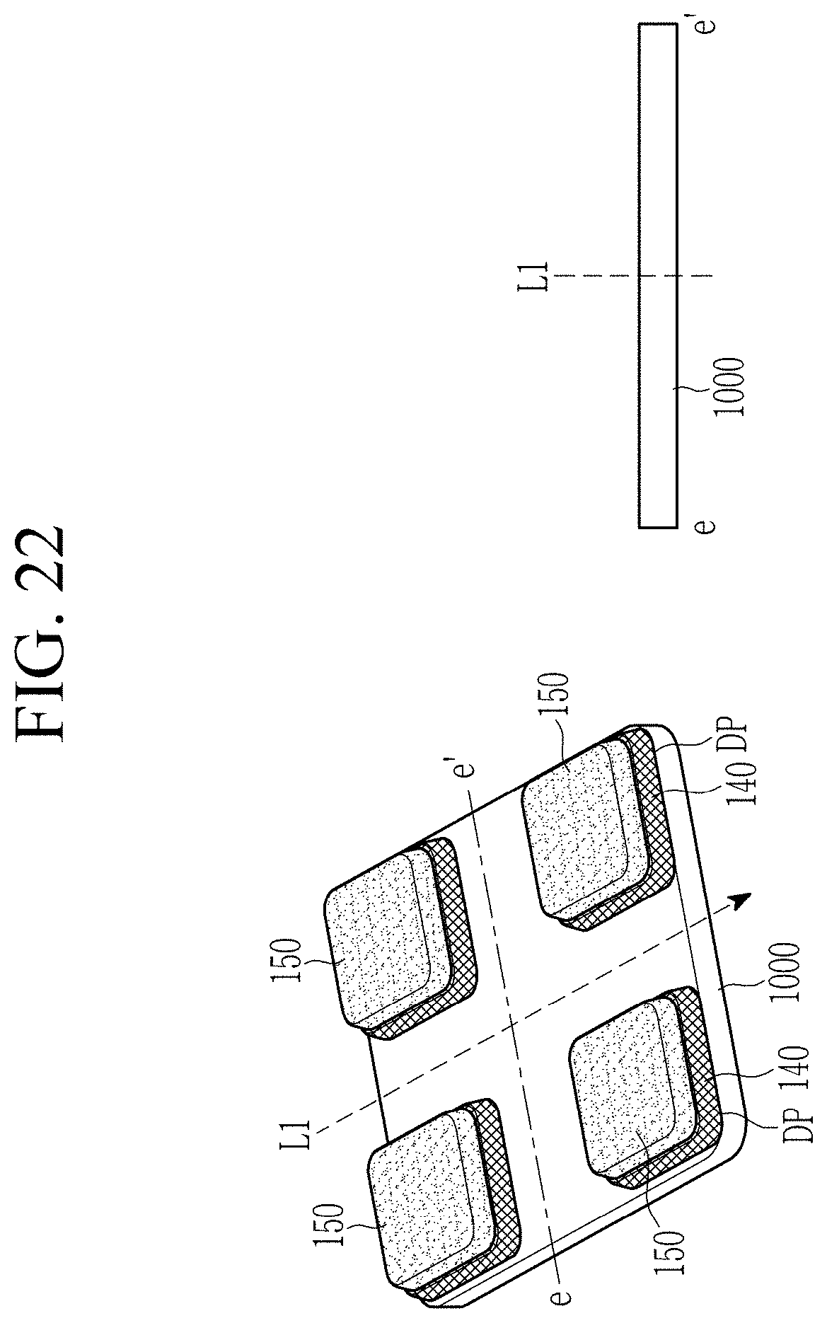
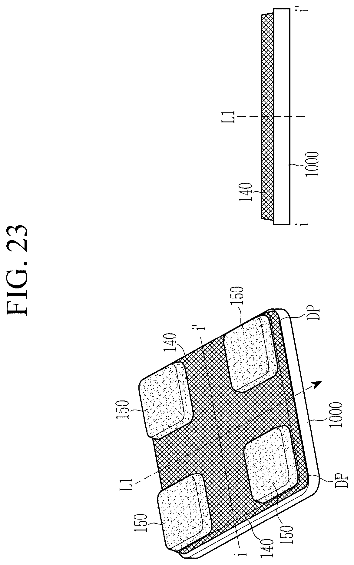
[0047] FIG. 21, FIG. 22, FIG. 23, and FIG. 24 illustrate the same region as FIG. 13 in a display device according to another embodiment of the present inventive concept.
DETAILED DESCRIPTION OF THE EMBODIMENTS
[0048] The present inventive concept will be described more fully hereinafter with reference to the accompanying drawings, in which embodiments of the inventive concept are shown. As those skilled in the art would realize, the described embodiments may be modified in various different ways, all without departing from the spirit or scope of the present disclosure.
[0049] Parts that are irrelevant to the description will be omitted to clearly describe the present disclosure, and like reference numerals designate like elements throughout the specification.
[0050] Further, in the drawings, the size and thickness of each element are arbitrarily illustrated for ease of description, and the present disclosure is not necessarily limited to those illustrated in the drawings. In the drawings, the thicknesses of layers, films, panels, regions, etc., are exaggerated for clarity. In the drawings, for ease of description, the thicknesses of some layers and areas are exaggerated.
[0051] It will be understood that when an element such as a layer, film, region, or substrate is referred to as being "on" another element, it can be directly on the other element or intervening elements may also be present. In contrast, when an element is referred to as being "directly on" another element, there are no intervening elements present. Further, in the specification, the word "on" or "above" means positioned on or below the object portion, and does not necessarily mean positioned on the upper side of the object portion based on a gravitational direction.
[0052] In addition, unless explicitly described to the contrary, the word "comprise" and variations such as "comprises" or "comprising" will be understood to imply the inclusion of stated elements but not the exclusion of any other elements.
[0053] Further, throughout the specification, the phrase "in a plan view" means viewing a target portion from the top, and the phrase "in a cross-sectional view" means viewing a cross-section formed by vertically cutting a target portion from the side.
[0054] Hereinafter, a display device and a manufacturing method thereof according to an embodiment of the present inventive concept will be described in detail with reference to the accompanying drawings. The present inventive concept may solve a problem that bubbles occur during a process of adhering a film to a lower portion of a substrate in a display device and in a manufacturing process thereof.
[0055] FIG. 1 illustrates a display device according to an embodiment of the present inventive concept. The display device according to the embodiment of FIG. 1 includes a plurality of display modules (DM1, DM2, DM3, . . . , DMn) disposed on a mother substrate 1000. That is, FIG. 1 illustrates the display device including the plurality of display modules (DM1, DM2, DM3, . . . , DMn) that may separately operate, and the display device may later be cut into individual display modules to function as respective display devices. The mother substrate 1000 may be a flexible substrate including polyimide.
[0056] FIG. 2 illustrates a cross-sectional view taken along line II-II' of FIG. 1. Referring to FIG. 2, the display device according to the present embodiment includes a mother film 2000 disposed under the mother substrate 1000. The mother film 2000 includes a first layer 2100 and a second layer 2200. The second layer 2200 may be disposed between the first layer 2100 and the mother substrate 1000.
[0057] The first layer 2100 may include polyethylene terephthalate (PET). In addition, the second layer 2200 may include a pressure sensitive adhesive (PSA). The PSA of the second layer 2200 adheres the first layer 2100 to the mother substrate 1000.
[0058] The mother film 2000 may be removed after the display device including the plurality of display modules is cut into individual display modules.
[0059] In the present inventive concept, a thickness of the first layer 2100 may be 60 .mu.m to 90 .mu.m, and a thickness of the second layer 2200 may be 40 .mu.m to 60 .mu.m. In the present inventive concept, the thickness of the first layer 2100 may be greater than that of the second layer 2200. When the thickness of the second layer 2200 is greater than that of the first layer 2100, a problem may occur in which an upper protective film 3000 is broken while the mother film 2000 is removed. In addition, an upper structure of the mother substrate 1000 may be damaged during the removing process of the mother film 2000.
[0060] In the present inventive concept, the second layer 2200 including the PSA has a thickness of 40 .mu.m to 60 .mu.m. Therefore, because the second layer 2200 has a sufficient thickness to be able to suppress occurrence of bubbles therein, the problem that the bubbles occur in the manufacturing process of the display device may be improved. Hereinafter, an effect of the present inventive concept together with the manufacturing process of the display device will be described in detail.
[0061] A manufacturing method of a display device according to an embodiment of the present inventive concept includes preparing a substrate including a plurality of display modules, and attaching the mother film 2000 to a rear surface of the substrate. The mother film 2000 includes the first layer 2100, and the second layer 2200 disposed between the first layer 2100 and the substrate 1000. The second layer 2200 may include the PSA, and its thickness may be from about 40 .mu.m to about 60 .mu.m. Thereafter, the manufacturing method may further include cutting the plurality of display modules into individual display modules and removing the mother film 2000.
[0062] That is, in the display device and the manufacturing method thereof according to the present inventive concept, because the mother film 2000 includes the second layer 2200 that has a multilayer structure, includes the PSA, and has a thickness of from about 40 .mu.m to about 60 .mu.m, it is possible to improve the problem that the bubbles occur during the manufacturing process of the display device.
[0063] Hereinafter, an effect of the present inventive concept will be described in detail with reference to the accompanying drawings.
[0064] FIG. 3 illustrates an enlarged view of a portion indicated by area A of FIG. 2 in detail. Referring to FIG. 3, a first inorganic film 110, a second inorganic film 120, an intermediate film 130, a first organic film 140, a second organic film 150, and a thin film encapsulation layer 160 are disposed on the mother substrate 1000. In FIG. 3, the structures of the inorganic films and the organic films are mainly shown, but a structure that is not shown may be further included.
[0065] Referring to FIG. 3, a display area DA, dams D1 and D2, and a dummy pattern DP are disposed on the mother substrate 1000 between adjacent individual display modules. The display area DA includes a display module and displays an image. Types of films stacked in the display area DA, the dams D1 and D2, and the dummy pattern DP may be different from each other, as shown in FIG. 3.
[0066] Referring to FIG. 3, the mother substrate 1000 is cut along a first cutting line L1 during a first cut. Thereafter, the cut mother substrate is cut along a second cutting line L2 during a second cut. That is, only one display area DA is disposed in the cut mother substrate through the first cut along the first cutting line L1, and the dummy pattern DP is eliminated through the second cut along the second cutting line L2.
[0067] Recently, in the display device, a bezel size has been reduced, and the display area has been gradually increased. In addition, because many display modules are prepared on one mother substrate 1000 during a manufacturing process for cost reduction, a distance between the display modules in the mother substrate 1000 is shortened. This means that distances between the first and second cutting lines L1 and L2 and the display area DA are shortened, and thus, bubbles are easily formed on the rear surface of the mother substrate 1000, and the bubbles are not easily eliminated. The bubbles on the rear surface of the mother substrate 1000 are formed during the process of attaching the mother film 2000 to the mother substrate 1000.
[0068] FIG. 4 illustrates a manufacturing process of a general display device. Referring to FIG. 4, a plurality of display modules DM1, DM2, and DM3 are disposed on the mother substrate 1000, and then the upper protective film 3000 is disposed thereon.
[0069] The mother film 2000 is attached to a lower side of the mother substrate 1000. The mother film 2000 is a film attached in a manufacturing process, and it may be removed in a final display device. The mother film 2000 may be attached by using a roller 7000. In the manufacturing process, it takes some time until cutting the mother film 2000 after attaching it to the display device. The waiting time varies depending on the manufacturing process, and it may be as short as 8 hours and as long as 100 hours or more. During the waiting time, the mother film 2000 lifts from the mother substrate 1000 to generate bubbles. In FIG. 4, the bubbles are generated between adjacent display modules which is indicated by an arrow.
[0070] However, the display device and the manufacturing method thereof according to the present embodiment prevent the formation of bubbles by setting the thickness of the second layer 2200 including the PSA from about 40 .mu.m to about 60 .mu.m.
[0071] FIG. 5 and FIG. 6 illustrate a principle in which bubbles occur in a display device according to a comparative example including the second layer 2200 having a thickness of about 25 .mu.m. Referring to FIG. 5, the mother film 2000 is attached to the display device by using a roller. Therefore, the mother substrate 1000 of the display device is pressed by a round surface of the roller, and is bent. This is because the mother substrate 1000 is a flexible substrate including a flexible material such as polyimide.
[0072] In a case in which the mother film 2000 is attached to the bent mother substrate 1000, when the thickness of the second layer 2200 serving as an adhesive is not sufficiently thick, the mother film 2000 is lifted at the bent portion of the mother substrate 1000 and bubbles are formed at the bent portion of the mother substrate 1000 which are indicated by an arrow.
[0073] FIG. 6 illustrates a cross-section of the display device in which the bubbles are formed. Referring to FIG. 6, bubbles occur when the mother substrate 1000 and the mother film 2000 are separated from each other at the bent portion of the mother substrate 1000.
[0074] FIG. 7 illustrates a cross-sectional view of a display device according to an embodiment of the present inventive concept, which is the same portion as those of FIG. 5 and FIG. 6. Referring to FIG. 7, in the display device according to the present embodiment, the thickness of the second layer 2200 of the mother film 2000 is from about 40 .mu.m to about 60 .mu.m, which is thicker than that of the comparative example.
[0075] Accordingly, as shown in FIG. 7, as the second layer 2200 fills the curved surface of the mother substrate 1000 without gap dispose between the mother substrate 1000 and the mother film 2000, the mother substrate remains attached. Therefore, it is possible to prevent the lifting of the mother film 2000 on the curved surface of the mother substrate 1000, and to suppress the occurrence of bubbles. In addition, as the thickness of the second layer 2200 increases, adhesive force also increases, and thus the mother substrate 1000 and the mother film 2000 are more strongly attached to each other and are not separated.
[0076] A bubble-occurring rate between the mother substrate 1000 and the mother film including the PSA was measured, and is shown in Table 1.
[0077] In Example 1, the thickness of the first layer 2100 including PET was about 75 .mu.m and the thickness of the second layer 2200 including the PSA was about 50 .mu.m. A bubble defect rate was measured after 32 hours had elapsed after the mother film 2000 was attached to the mother substrate 1000. FIG. 8 illustrates a result of an experiment according to Example 1.
TABLE-US-00001 TABLE 1 Example 1 Stagnation time 32 h 100 h Thickness of film layer 75/50 75/50 (.mu.m) (PET/PSA) Mother panel bubble Not occurring 0% Not occurring 0% defect rate (0/46 substrate) (0/46 substrate)
[0078] The measurement of the bubble defect rate was calculated by the number of substrates in which bubbles occurred among test target substrates. In Example 1 in which the thickness of the second layer 2200 containing the PSA was about 50 .mu.m, the phenomenon of bubble occurrence after 32 hours was improved. That is, in Example 1, no bubbles were observed in any of the 46 substrates. Referring to FIG. 8, it was confirmed that almost no bubbles were formed in the display device. Referring back to Table 1, in the display device according to Example 1, no bubbles were observed even after 100 hours had elapsed, and it was confirmed that the phenomenon of bubble occurrence was improved.
[0079] That is, the display device and the manufacturing method thereof according to the present embodiment have the increased thickness of the second layer 2200 including the PSA in the mother film 2000, so that the adhesive force between the mother substrate 1000 and the mother film 2000 is increased, and the second layer 2200 completely fills the curved portion of the mother substrate 1000. Accordingly, it is possible to prevent the occurrence of bubbles between the mother substrate 1000 and the mother film 2000.
[0080] Hereinafter, a manufacturing method of a display device according to another embodiment of the present inventive concept will be described. The display device and the manufacturing method thereof that are previously described relate to a mother substrate in which a plurality of display modules are formed on one substrate, and the manufacturing method of the display device according to the present embodiment includes a process of cutting the mother substrate on which the plurality of display modules are located into individual display modules.
[0081] That is, the manufacturing method of the display device according to the present embodiment includes preparing a substrate which includes a plurality of display modules and dummy patterns disposed between the display modules in a plan view and cutting the substrate along a cutting line to separate the substrate into individual display modules, wherein the dummy pattern is disposed along the cutting line, and a groove in which a second organic film 150 is eliminated in the dummy pattern is positioned in a direction perpendicular to the cutting line.
[0082] Thereafter, the manufacturing method may further include forming a protective layer on the rear surface of the substrate. Bubbles occurring in the forming of the protective layer may be easily eliminated in the direction of the cutting line through the groove located in the dummy pattern.
[0083] In the present embodiment, the substrate prepared in the preparing of the substrate including the plurality of display modules may be the substrate manufactured according to the manufacturing method of the foregoing embodiment. That is, the substrate prepared in the preparing of the substrate including the plurality of display modules may be a substrate manufactured by preparing the mother substrate 1000 including the plurality of display modules and attaching the mother film 2000 to the rear surface of the mother substrate 1000.
[0084] In this case, the mother film 2000 may include the first layer 2100 and the second layer 2200 disposed between the first layer 2100 and the substrate 1000, and the second layer 2200 may include the PSA and have a thickness of from about 40 .mu.m to about 60 .mu.m.
[0085] Bubbles may not be formed on the rear surface of the substrate including the plurality of display modules manufactured in this manner. However, even though the mother substrate is prepared without bubbles in the rear surface thereof, bubbles may be formed when the protective layer is attached after the mother substrate is cut into individual substrates. The manufacturing method of the display device according to the present embodiment prevents bubbles occurring in the process of attaching the protective layer after cutting the mother substrate into individual substrates.
[0086] FIG. 9 and FIG. 10 respectively illustrate a process in which the display device of FIG. 3 is cut. FIG. 9 illustrates a cross-sectional view of a general display device cut along the first cutting line L1 of FIG. 3. Then, it is cut along the second cutting line L2. In this case, in FIG. 9, because a structure such as the dummy pattern DP is not disposed near the second cutting line L2, the bubbles occurring when the protective layer is attached to the rear surface of the substrate 1000 may be eliminated.
[0087] However, recently, because the size of a bezel of a display device is minimized, a cross-section as shown in FIG. 10 is provided. Referring to FIG. 10, the dummy pattern DP is disposed near the second cutting line L2. Therefore, a passage through which bubbles can be removed is formed when the protective layer is attached to the rear surface. That is, the bubble-eliminating passage is blocked by the dummy pattern DP, and thus the bubbles are not easily eliminated. This is because, although the dummy pattern DP corresponds to a structure positioned on the substrate 1000 and the protective layer corresponds to a structure attached to the rear surface of the substrate, contact properties between the protective layer on the rear surface of the substrate and the substrate are affected by the structure on the substrate 1000. Therefore, by changing a design of a structure of an upper surface of the substrate 1000, it is possible to eliminate the bubbles in the protective layer located on the rear surface of the substrate.
[0088] FIG. 11 illustrates a region where bubbles occur in a display device which is cut to include one display module. An area indicated by `B` in FIG. 11 is an area where bubbles are prone to occur.
[0089] FIG. 12 schematically illustrates a manufacturing method of a display device according to an embodiment. Referring to FIG. 12, the mother film 2000 on which the plurality of display modules DM1, DM2, and DM3 are disposed is first attached to the rear surface of the mother substrate 1000. The upper protective film 3000 is formed on the plurality of display modules DM1, DM2, and DM3.
[0090] The mother film 2000 may be attached by roll lamination using the roller 7000, and the mother film 2000 may include the first layer 2100 and the second layer 2200. The first layer 2100 may include PET and have a thickness of from about 60 .mu.m to about 90 .mu.m, and the second layer 2200 may include the PSA and may have a thickness of from about 40 .mu.m to about 60 .mu.m.
[0091] Next, referring to FIG. 12, the mother substrate 1000 is cut to separate the plurality of display modules into individual display modules.
[0092] Then, the mother film 2000 under the mother substrate 1000 is removed.
[0093] Subsequently, a protective layer 4000 is attached on the rear surface of the substrate 1000 from which the mother film 2000 is removed. In this case, the protective layer 4000 may be of a film type, and may be attached by roll lamination using the roller 7000. Bubbles may be formed in the process of attaching the protective layer 4000 on an alignment mark of the display device, thereby obstructing a subsequent alignment process.
[0094] Thus, the manufacturing method of the display device according to the present embodiment is a manufacturing method that may easily eliminate bubbles occurring when the protective layer 4000 is attached.
[0095] FIG. 13 illustrates a display device according to an embodiment of the present inventive concept. Referring to FIG. 13, the dummy pattern DP which includes an inorganic film 120, an intermediate film 130, a first organic film 140 and a second organic film 150 is disposed to overlap the cutting line L1. In this case, a portion of the second organic film 150 is removed along a direction b-b' extending perpendicular to the cutting line L1 to expose the first organic film 140. A valley is formed between adjacent second organic films 150.
[0096] The bubbles may be discharged through the valley. FIG. 14 illustrates an image near a cutting line of the display device according to the embodiment of FIG. 13. Referring to FIG. 14, the valley is indicated by an arrow. In the present embodiment, a width of the valley is about 0.5 mm. As can be seen in FIG. 13, the bubbles near the cutting line may be discharged through the valley.
[0097] FIG. 13 illustrates a structure in which the first organic film 140 which is disposed under the second organic film 140 is not removed, but in another embodiment, the first organic film 140 may also be removed. That is, as shown in FIG. 15, when the first organic film 140 is removed, the bubbles may be well discharged through a valley formed by removing the second organic film 150 and the first organic film 140.
[0098] FIG. 16 illustrates the same area as FIG. 13 in another embodiment of the present inventive concept. Referring to FIG. 16, the display device according to the present embodiment is the same as the display device of FIG. 13, except that an area in which the second organic film 150 is eliminated is larger than that in FIG. 13. A detailed description of the same components will be omitted.
[0099] FIG. 17 illustrates an image near a cut plane of the display device according to the embodiment of FIG. 16. Referring to FIG. 17, in the display device according to the embodiment, a width of the second organic film 150 eliminated is about 4.15 nm. In this case, the bubble was completely eliminated, and it was confirmed that the alignment mark indicated by a dotted circle in FIG. 17 was clearly seen without being covered by the bubbles.
[0100] FIG. 16 illustrates a structure in which the first organic film 140 is not removed and the second organic film 150 is partially removed, but the first organic film 140 may also be removed. That is, as shown in FIG. 18, when the first organic film 140 is removed, the bubbles may be well discharged.
[0101] FIG. 19 illustrates an image in which bubbles occur such that an alignment mark is covered by the bubbles according to a comparative example of the present inventive concept. FIG. 20 illustrates an image in which no alignment mark is covered by the bubbles because no bubbles occur according to an embodiment of the present inventive concept. Comparing FIG. 19 with FIG. 20, it can be seen that in FIG. 19, the alignment mark is covered by the bubbles, so it is hard to be recognized (see the dashed circle portion), but in FIG. 20, there are no bubbles, so the alignment mark is clearly recognized (see the dashed circle portion).
[0102] Therefore, in the manufacturing method of the display device according to the present embodiment, it is desirable that the area in which the second organic film 150 is recognized overlaps the alignment mark. When the groove of the dummy pattern DP in which the second organic film 150 is recognized overlaps the alignment mark, it is possible to prevent the alignment mark from being covered by the bubbles because the bubbles are removed through the valley in which the first organic film or the second organic film 150 is removed.
[0103] FIG. 21 to FIG. 23 illustrate display devices according to other embodiments. Referring to FIG. 21, the display device according to the present embodiment is the same as the display device according to the embodiment of FIG. 13, except that the first organic film and the second organic film 150 in the dummy pattern DP in an area overlapping the cutting line L1 is also removed. A detailed description of the same components will be omitted.
[0104] Referring to the cross-sectional view taken along line d-d' of FIG. 21, when the portion of the second organic film 150 is removed and the first organic film 140 and the second organic film 150 are removed at a portion overlapping the cutting line L1, the bubbles may be more easily removed.
[0105] The display device of FIG. 22 is the same as the display device according to the embodiment of FIG. 21, except that both the second organic film 150 and the first organic film 140 are removed along a line e-e' too. In FIG. 22, because both the first organic film 140 and the second organic film 150 are removed in the direction perpendicular to the cutting line L1, the bubbles may be more easily removed.
[0106] The embodiment of FIG. 23 is the same as that of FIG. 21 except that the first organic film 140 is not removed at the cutting line L1. A detailed description of the same components will be omitted.
[0107] The embodiment of FIG. 24 is the same as that of FIG. 21, except that the first organic film 140 and the second organic film 150 are eliminated in the direction perpendicular to the cutting line L1. In FIG. 24, no organic film is disposed in the passage through which the bubbles are discharged, so that the bubbles may be well discharged.
[0108] The protective layer is a structure attached to the rear surface of the substrate 1000 and the dummy pattern DP is a structure disposed on the upper surface of the substrate, but the passage through which the bubbles formed on the rear surface of the substrate 1000 are discharged is affected by the structure disposed on the upper surface. Therefore, when the passage through which the bubbles may be discharged is formed in the dummy pattern DP as in the manufacturing method according to the present embodiment, the bubbles formed when the protective layer is attached on the rear surface of the substrate 1000 may be easily removed.
[0109] As described above, according to the display device and the manufacturing method thereof according to the embodiment of the present inventive concept, by increasing the thickness of the mother film 2000 which may be removed during the manufacturing process, it is possible to improve the problem that the mother substrate 1000 and the mother film 2000 are detached from each other to form bubbles between the mother substrate 1000 and the mother film 2000 during the prolonged waiting time in the manufacturing process. In addition, the groove is formed in the dummy pattern near the cutting line in the direction perpendicular to the cutting line, and thus, the passage through which the bubbles formed between the mother substrate 1000 and the rear protective layer may be discharged is formed, so that the bubbles may be effectively removed.
[0110] While this inventive concept has been described in connection with what is presently considered to be practical embodiments, it is to be understood that the inventive concept is not limited to the disclosed embodiments, but, on the contrary, is intended to cover various modifications and equivalent arrangements included within the spirit and scope of the appended claims.
* * * * *
D00000
D00001
D00002
D00003
D00004
D00005
D00006
D00007
D00008
D00009
D00010
D00011
D00012

D00013

D00014

D00015

D00016

D00017

D00018

D00019

D00020

D00021
D00022
D00023

XML
uspto.report is an independent third-party trademark research tool that is not affiliated, endorsed, or sponsored by the United States Patent and Trademark Office (USPTO) or any other governmental organization. The information provided by uspto.report is based on publicly available data at the time of writing and is intended for informational purposes only.
While we strive to provide accurate and up-to-date information, we do not guarantee the accuracy, completeness, reliability, or suitability of the information displayed on this site. The use of this site is at your own risk. Any reliance you place on such information is therefore strictly at your own risk.
All official trademark data, including owner information, should be verified by visiting the official USPTO website at www.uspto.gov. This site is not intended to replace professional legal advice and should not be used as a substitute for consulting with a legal professional who is knowledgeable about trademark law.