Power Amplifier And Radio Frequency Device Comprising The Same
WANG; Zhancang ; et al.
U.S. patent application number 16/955746 was filed with the patent office on 2021-01-14 for power amplifier and radio frequency device comprising the same. This patent application is currently assigned to Telefonaktiebolaget LM Ericsson (publ). The applicant listed for this patent is Telefonaktiebolaget LM Ericsson (publ). Invention is credited to Zhancang WANG, Dan YAN.
| Application Number | 20210013838 16/955746 |
| Document ID | / |
| Family ID | 1000005151696 |
| Filed Date | 2021-01-14 |


View All Diagrams
| United States Patent Application | 20210013838 |
| Kind Code | A1 |
| WANG; Zhancang ; et al. | January 14, 2021 |
POWER AMPLIFIER AND RADIO FREQUENCY DEVICE COMPRISING THE SAME
Abstract
A power amplifier is disclosed for amplifying an input signal and providing an amplified signal to a load at a junction node. The power amplifier comprises a splitter network, a carrier amplifier path and a peaking amplifier path. The peaking amplifier path comprises a first impedance transformer coupled between a peaking output matching network and the junction node to enhance the off-state impedance of the peaking amplifier. The carrier amplifier path comprises a second impedance transformer coupled between a carrier output matching network and the junction node.
| Inventors: | WANG; Zhancang; (Beijing, CN) ; YAN; Dan; (Beijing, CN) | ||||||||||
| Applicant: |
|
||||||||||
|---|---|---|---|---|---|---|---|---|---|---|---|
| Assignee: | Telefonaktiebolaget LM Ericsson
(publ) Stockholm SE |
||||||||||
| Family ID: | 1000005151696 | ||||||||||
| Appl. No.: | 16/955746 | ||||||||||
| Filed: | December 19, 2017 | ||||||||||
| PCT Filed: | December 19, 2017 | ||||||||||
| PCT NO: | PCT/CN2017/117128 | ||||||||||
| 371 Date: | June 18, 2020 |
| Current U.S. Class: | 1/1 |
| Current CPC Class: | H04B 2001/0416 20130101; H03F 2200/451 20130101; H04B 1/40 20130101; H03F 2200/222 20130101; H03F 2200/387 20130101; H03F 3/211 20130101; H04B 1/04 20130101; H03F 1/56 20130101; H04W 88/08 20130101; H03F 1/0288 20130101 |
| International Class: | H03F 1/02 20060101 H03F001/02; H03F 3/21 20060101 H03F003/21; H03F 1/56 20060101 H03F001/56; H04B 1/04 20060101 H04B001/04; H04B 1/40 20060101 H04B001/40 |
Claims
1. A power amplifier comprising: a splitter network configured to split an input signal into a carrier input signal and a peaking input signal; a carrier amplifier path comprising at least a carrier amplifier configured to amplify the carrier input signal and carrier input and output matching networks; and a peaking amplifier path combined at a junction node with the carrier amplifier path and comprising at least a peaking amplifier configured to amplify the peaking input signal and peaking input and output matching networks; wherein the peaking amplifier path further comprises a first impedance transformer coupled between an output of the peaking output matching network and the junction node to enhance the off-state impedance of the peaking amplifier; and wherein the carrier amplifier path further comprises a second impedance transformer coupled between an output of the carrier output matching network and the junction node.
2. The power amplifier according to claim 1, wherein the saturation output power ratio between the peaking amplifier and the carrier amplifier is equal to or greater than one.
3. The power amplifier according to claim 2, wherein the first impedance transformer is configured to transform a first output impedance seen from the output of the peaking output matching network into a second output impedance seen from an output of the first impedance transformer, the second output impedance being higher than the first output impedance; wherein the second impedance transformer is configured to transform a third output impedance seen from the output of the carrier output matching network into a fourth output impedance seen from an output of the second impedance transformer; and wherein the parallel impedance of the second and fourth output impedances equals to a junction node impedance of the power amplifier in both a high-power mode where both the carrier and peaking amplifiers turn on and a low-power mode where only the carrier amplifier turns on, and the junction node impedance equals to the system load impedance of the power amplifier.
4. The power amplifier according to claim 3, wherein when the power amplifier operates in the low-power mode where the peaking amplifier is turned off, the second output impedance equals to the first output impedance multiplied by at least a product of voltage standing wave ratio (VSWR) and r, where r is the saturation output power ratio between the peaking amplifier and the carrier amplifier, and VSWR=r+1.
5. The power amplifier according to claim 4, wherein when the power amplifier oprates in the high-power mode, the first output impedance equals to Z0/r, the second output impedance equals to Z0*VSWR, the third output impedance equals to Z0, and the fourth output impedance equals to Z0*VSWR*r, where Z0 equals to ZL/r and ZL is the system impedance of the power amplifier; and wherein when the power amplifier operates in the low-power mode, the third output impedance equals to Z0*VSWR, and the fourth output impedance equals to Z0*r.
6. The power amplifier according to claim 5, wherein the carrier amplifier path is configured to have low impedance transformation ratios in both the high-power mode and the low-power mode to expand bandwith.
7. The power amplifier according to claim 1, wherein the splitter network is configured to split the power of the input signal in an imbalanced manner to assign more power to the peaking amplifier path and assign less power to the carrier amplifier path.
8. The power amplifier according to claim 7, wherein the splitter network is one of: an in-phase power divider, a directional coupler, and a hybrid coupler.
9. The power amplifier according to claim 1, wherein an offset line is disposed either in the carrier amplifier path before the carrier input matching network, or in the peaking amplifier path before the peaking input matching network.
10. The power amplifier according to claim 1, wherein the first impedance transformer is disposed partially within the peaking output matching network.
11. A radio unit (RU) comprising the power amplifier according to claim 1.
12. canceled
13. A base station comprising: a processor; a memory, the memory containing instructions executable by the processor to implement functions of the base station; the power amplifier according to claim 1 wherein the power amplifier is configured to amplify a radio frequency (RF) signal; and an antenna unit configured to transmit the amplified RF signal.
14. A terminal device comprising: a processor; a memory, the memory containing instructions executable by the processor to implement functions of the terminal device; the power amplifier according to claim 1, wherein the power amplifier is configured to amplify a radio frequency (RF) signal; and an antenna unit configured to transmit the amplified RF signal.
Description
TECHNICAL FIELD
[0001] Embodiments of the disclosure generally relate to the field of electronic components, and, more particularly, to a power amplifier and a radio frequency device comprising the same.
BACKGROUND
[0002] This section introduces aspects that may facilitate better understanding of the present disclosure. Accordingly, the statements of this section are to be read in this light and are not to be understood as admissions about what is in the prior art or what is not in the prior art.
[0003] In cellular base stations of 4G and beyond, advanced digital modulation schemes are u ed for high spectrum efficiency. The corresponding radio frequency (RF) signal exhibits a large peak to average power ratio (PAPR), which is amplified simultaneously in a power amplifier (PA). Therefore, the instantaneous transmitting power will vary extensively and fast. Due to the high PAPR stimulus, traditional RF PAs would suffer from rather low average efficiency.
[0004] One way for increasing the efficiency of an RF PA is to use Doherty architecture. For example, the classic Doherty PA may be used to enhance the efficiency for moderate PAPR signal, which creates a second efficiency peak point at 6 dB far away from the peak output power during back-offs. However, with ever increasing PAPR, it is difficult for the classic Doherty PA to maintain high efficiency with PAPR greater than 6 dB due to the limited Doherty region.
[0005] To achieve a Doherty region with greater than 6 dB high efficiency range, the Doherty architecture has been extended to inverted asymmetric Doherty variants which use different power levels of transistors and an inverted load modulation network. This may bring about simplified output matching configuration and realize more compact design from the drain terminal to the final output. One parameter of an inverted asymmetric Doherty PA that may affect the power added efficiency (PAE) is peaking amplifier off-state impedance. It refers to the impedance looking back into the peaking amplifier, including the output matching network, when the peaking amplifier is in an off state. The ideal off-state impedance should be relatively high so as not to load the carrier amplifier during a low input power condition where the peaking amplifier is turned off.
[0006] Therefore, it would be desirable to provide a Doherty PA with enhanced peaking amplifier off-state impedance.
SUMMARY
[0007] This summary is provided to introduce a selection of concepts in a simplified form that are further described below in the detailed description. This summary is not intended to identify key features or essential features of the claimed subject matter, nor is it intended to be used to limit the scope of the claimed subject matter.
[0008] One of the objects of the disclosure is to provide a power amplifier with enhanced peaking off-state impedance.
[0009] According to one aspect of the disclosure, there is provided a power amplifier. The power amplifier comprises a splitter network, a carrier amplifier path and a peaking amplifier path. The splitter network is configured to split an input signal into a carrier input signal and a peaking input signal. The carrier amplifier path comprises at least a carrier amplifier configured to amplify the carrier input signal and carrier input and output matching networks. The peaking amplifier path is combined at a junction node with the carrier amplifier path and comprises at least a peaking amplifier configured to amplify the peaking input signal and peaking input and output matching networks. The peaking amplifier path further comprises a first impedance transformer coupled between an output of the peaking output matching network and the junction node to enhance the off-state impedance of the peaking amplifier. The carrier amplifier path further comprises a second impedance transformer coupled between an output of the carrier output matching network and the junction node.
[0010] In an embodiment of the disclosure, the saturation output power ratio between the peaking amplifier and the carrier amplifier is equal to or greater than one.
[0011] In an embodiment of the disclosure, the first impedance transformer is configured to transform a first output impedance seen from the output of the peaking output matching network into a second output impedance seen from an output of the first impedance transformer. The second output impedance is higher than the first output impedance. The second impedance transformer is configured to transform a third output impedance seen from the output of the carrier output matching network into a fourth output impedance seen from an output of the second impedance transformer. The parallel impedance of the second and fourth output impedances equals to a junction node impedance of the power amplifier in both a high-power mode where both the carrier and peaking amplifiers turn on and a low-power mode where only the carrier amplifier turns on. The junction node impedance equals to the system load impedance of the power amplifier.
[0012] In an embodiment of the disclosure, when the power amplifier operates in the low-power mode where the peaking amplifier is turned off, the second output impedance equals to the first output impedance multiplied by at least a product of voltage standing wave ratio (VSWR) and r, where r is the saturation output power ratio between the peaking amplifier and the carrier amplifier, and VSWR=r+1.
[0013] In an embodiment of the disclosure, when the power amplifier operates in the high-power mode, the first output impedance equals to Z.sub.0/r, the second output impedance equals to Z.sub.0*VSWR, the third output impedance equals to Z.sub.0, and the fourth output impedance equals to Z.sub.0*VSWR*r, where Z.sub.0 equals to Z.sub.L/r and Z.sub.L is the system impedance of the power amplifier. When the power amplifier operates in the low-power mode, the third output impedance equals to Z.sub.0*VSWR, and the fourth output impedance equals to Z.sub.0*r.
[0014] In an embodiment of the disclosure, the carrier amplifier path is configured to have low impedance transformation ratios in both the high-power mode and the power mode to expand bandwith.
[0015] In an embodiment of the disclosure, the splitter network is configured to split the power of the input signal in an imbalanced manner to assign more power to the peaking amplifier path and assign less power to the carrier amplifier path.
[0016] In an embodiment of the disclosure, the splitter network is one of: an in-phase power divider, a directional coupler, and a hybrid coupler.
[0017] In an embodiment of the disclosure, an offset line is disposed either in the carrier amplifier path before the carrier input matching network, or in the peaking amplifier path before the peaking input matching network.
[0018] In an embodiment of the disclosure, the first impedance transformer is disposed partially within the peaking output matching network.
[0019] According to another aspect of the disclosure, there is provided a radio unit (RU) comprising the power amplifier according to the above aspect.
[0020] In an embodiment of the disclosure, the RU is used for a base station or a terminal device.
[0021] According to another aspect of the disclosure, there is provided a base station. The base station comprises a processor, a memory, the power amplifier according to the above aspect and an antenna unit. The memory contains instructions executable by the processor to implement functions of the base station. The power amplifier is configured to amplify an RF signal. The antenna unit is configured to transmit the amplified RF signal.
[0022] According to another aspect of the disclosure, there is provided a terminal device. The terminal device comprises a processor, a memory, the power amplifier according to the above aspect and an antenna unit. The memory contains instructions executable by the processor to implement functions of the terminal device. The power amplifier is configured to amplify an RF signal. The antenna unit is configured to transmit the amplified RF signal.
[0023] According to some embodiment(s) of the disclosure, due to enhanced peaking off-state impedance, the power leakage from the carrier amplifier to the peaking amplifier path can be reduced. Thereby, the carrier amplifier back-off efficiency can be enhanced.
BRIEF DESCRIPTION OF THE DRAWINGS
[0024] These and other objects, features and advantages of the disclosure will become apparent from the following detailed description of illustrative embodiments thereof, which are to be read in connection with the accompanying drawings.
[0025] FIG. 1 is a diagram showing an existing Doherty PA;
[0026] FIG. 2 is a diagram showing an existing Doherty PA;
[0027] FIG. 3 is a diagram showing an existing Doherty PA;
[0028] FIGS. 4A-4B are schematic diagrams showing a Doherty PA according to an embodiment of the disclosure under different operation modes;
[0029] FIGS. 5A-5B show a design example for the load modulation network shown in FIGS. 4A-4B;
[0030] FIG. 6 shows the improved impedance transformation ratios of an embodiment of the disclosure compared with a classic Doherty PA;
[0031] FIG. 7 shows a simulated design example for the Doherty PA shown in FIGS. 4A-4B;
[0032] FIG. 8 shows the transducer gain and PAE of the simulated design example;
[0033] FIG. 9 shows the characteristics of an input signal with high PAPR;
[0034] FIGS. 10A-10D show the characteristics of the simulated design example under the input signal shown in FIG. 9;
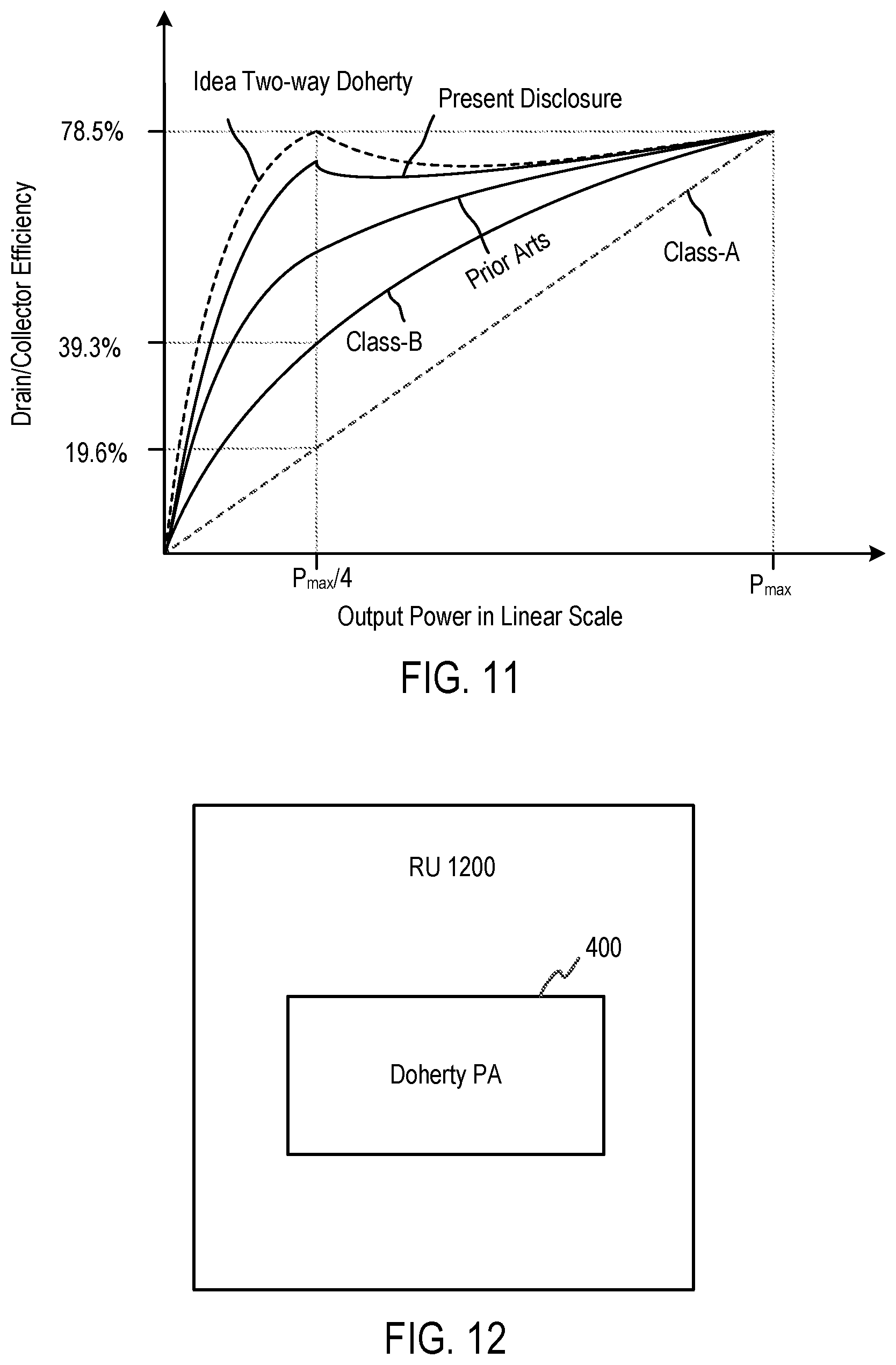
[0035] FIG. 11 shows the efficiency curves of different Doherty PAs;
[0036] FIG. 12 is a block diagram showing a radio unit according to an embodiment of the disclosure;
[0037] FIG. 13 is a block diagram showing a base station according to an embodiment of the disclosure; and
[0038] FIG. 14 is a block diagram showing a terminal device according to an embodiment of the disclosure;
DETAILED DESCRIPTION
[0039] For the purpose of explanation, details are set forth in the following description to provide a thorough understanding of the embodiments disclosed. It is apparent, however, to those skilled in the art that the embodiments may be implemented without these specific details or with an equivalent arrangement.
[0040] As mentioned above, peaking amplifier off-state impedance is an important parameter that can affect the power added efficiency (PAE) of an inverted asymmetric Doherty PA. However, the amplifier topologies in current technologies can only maintain a moderate peaking amplifier off-state impedance for high power applications, because their traditional configurations limit further enhancing of the peaking off-state impedance. Due to a lower than desired peaking path off-state impedance, the carrier/main amplifier back-off efficiency may be compromised.
[0041] Specifically, for the existing solution shown in FIG. 1, to achieve enhanced peaking off-state impedance, the inverted Doherty PA 100 requires the impedance value Zo of the impedance inverter 122 to be greater than the load impedance Z.sub.L. However, using high characteristic impedance Zo for the impedance inverter 122 may bring about the matching difficulty for the main/carrier amplifier 106 in both output matching optimizations for full power and back-off power modes.
[0042] For the existing solution shown in FIG. 2, more power is split and driven into the peaking amplifier for power matching, which can help the peaking amplifier to realize full power. However, the more power is assigned to the peaking path, the more difficult it is to realize high peaking off-state impedance. For example, for high power Gallium Nitride (GaN) high electron mobility transistor (HEMT) PA scenario, the overall Doherty gain, amplitude-to-amplitude conversion (AM-AM) response and peaking off-state impedance would be degraded. In practical design for commercial products in base stations with GaN HEMTs, it may bring about difficulties to meet the transducer gain and high efficiency for main/carrier amplifier back-offs.
[0043] For the existing solution shown in FIG. 3, a 3 dB hybrid coupler plus an attenuator are used in the main/carrier path, which may help to improve amplitude-to-amplitude conversion (AM-AM) response and make the peaking amplifier reach its full power. However, it may reduce the overall Doherty gain too much by introducing the attenuation in the main/carrier path. Also, the peaking off-state impedance may be degraded due to more input power for the peaking amplifier. To compensate the impact of the uneven power splitting, the input/gate bias of the peaking amplifier may need to be very negative bias in GaN HEMT PAs, resulting in that the AM-AM response would be quite difficult to be linearized or accepted in product specifications.
[0044] The present disclosure proposes an improved solution for Doherty PA with high peaking off-state impedance. Hereinafter, the solution will be described in detail with reference to FIGS. 4-12.
[0045] FIGS. 4A-4B are schematic diagrams showing a Doherty PA according to an embodiment of the disclosure under different operation modes. As shown, the Doherty PA 400 comprises a splitter network 402, a carrier amplifier path 404, a peaking amplifier path 406 and a load 408. The carrier amplifier path 404 and the peaking amplifier path 406 are connected respectively to the two output ports of the splitter network 402 and are combined at a junction node J. The load 408 is coupled to the junction node J and has the system impedance Z.sub.L which is typically 50 Ohm.
[0046] The carrier amplifier path 404 comprises a carrier input matching network 4042, a carrier amplifier 4041, a carrier output matching network 4043, a second impedance transformer 4044 connected in series in the described order. The peaking amplifier path 406 comprises an offset line 4065, a peaking input matching network 4062, a peaking amplifier 4061, a peaking output matching network 4063 and a first impedance transformer 4064 connected in series in the described order.
[0047] The splitter network 402 is configured to split an input signal into a carrier input signal and a peaking input signal. It can split the power of the input signal in an imbalanced manner to assign more power to the peaking amplifier path 406 and assign less power to the carrier amplifier path 404. That is, the carrier amplifier 4041 and the peaking amplifier 4061 deliver unequal amount of output power at the maximum drive condition. For example, the splitter network 402 may split the input power into 1:N ratio between the carrier amplifier path and the peaking amplifier path, where N is an integer greater than one.
[0048] As a first example, the splitter network 402 may be a hybrid coupler that splits the input signal such that the carrier input signal and the peaking input signal has a 90-degree phase difference. As a second example, the splitter network 402 may be a directional coupler that splits the input signal such that the carrier input signal and the peaking input signal has an equalized/arbitrary phase difference. As a third example, the splitter network 402 may be an in-phase power divider that splits the input signal such that the carrier input signal and the peaking input signal has a phase difference of zero degree. In the second and third examples, compared to the first example having a 90-degree phase difference, the offset line for compensating the phase difference can be made shorter to achieve a more compact size.
[0049] The carrier amplifier 4041 is configured to amplify the carrier input signal. It is turned on in both a high-power mode (also referred to as full power mode) and a low-power mode (also referred to as back-off power mode). As an exemplary example, the carrier amplifier 4041 may be implemented by using class -E, -F, or -F.sup.-1 mode amplifier such as GaN HEMT. It should be noted that the present disclosure is not limited to this example and any other suitable transistor may be used instead.
[0050] The carrier input matching network 4042 is configured to match the input impedance of the carrier amplifier 4041 to the system impedance of the Doherty PA 400. The system impedance may typically take the value of 50 Ohm. The carrier output matching network 4043 is configured to match the output impedance of the carrier amplifier 4041 to two corresponding impedances for the high-power mode and the low-power mode respectively.
[0051] The peaking amplifier 4061 is configured to amplify the peaking input signal. It is turned on in the high-power mode and is turned off in the low-power mode. The saturation output power ratio (denoted as r) between the peaking amplifier 4061 and the carrier amplifier 4041 is equal to or greater than one, that is, r.gtoreq.1. In other words, the Doherty PA 400 is an asymmetric Doherty PA. Similar to the carrier amplifier 4041, the peaking amplifier 4061 may be implemented by using, but not limited to, class -E, -F, or -F.sup.-1 mode amplifier such as GaN HEMT.
[0052] The peaking input matching network 4062 is configured to match the input impedance of the peaking amplifier 4061 to the system impedance of the Doherty PA 400. The peaking output matching network 4063 is configured to match the output impedance of the peaking amplifier 4061 to two corresponding impedances for the high-power mode and the low-power mode respectively.
[0053] The offset line 4065 is configured to compensate the phase difference between the carrier amplifier path 404 and the peaking amplifier path 406 to guarantee the phase synchronization during combination at the junction node J. Alternatively, instead of being disposed in only the peaking amplifier path 406, an offset line may be disposed in only the carrier amplifier path 404 before the carrier input matching network 4042.
[0054] The first impedance transformer 4064 is configured to transform a first output impedance (denoted as Z.sub.out1) seen from the output of the peaking output matching network 4063 into a second output impedance (denoted as Z.sub.out2) that is seen from an output of the first impedance transformer 4064 and higher than Z.sub.out1. The first impedance transformer 4064 may be implemented as a quarter wave transmission line. Optionally, the first impedance transformer 4064 may be disposed partially within (or partially absorbed by) the peaking output matching network 4063 to minimize the size of the Doherty PA 400.
[0055] The second impedance transformer 4044 is configured to transform a third output impedance (denoted as Z.sub.out3) seen from the output of the carrier output matching network 4043 into a fourth output impedance (denoted as Z.sub.out4) seen from an output of the second impedance transformer 4044. The second impedance transformer 4044 may be implemented as a quarter wave transmission line.
[0056] The parallel impedance of Z.sub.out2 and Z.sub.out4 equals to a junction node impedance (denoted as Z.sub.J) of the Doherty PA 400 in both the high-power mode and the low-power mode. In this way, the impedance Z.sub.out2 happening in the peaking amplifier path 406 can be accommodated by the second impedance transformer 4044. Furthermore, the junction node impedance Z.sub.J equals to the system impedance (denoted as Z.sub.L) which may typically take the value of 50 Ohm. This can make the design compact and save an additional impedance transformer for transforming the junction node impedance into the system impedance.
[0057] For example, in the high-power mode shown in FIG. 4A, it is assumed that the output impedance of the peaking amplifier 4061 is denoted as Z'.sub.opt , and Z.sub.out1 from the peaking output matching network 4063 is denoted as Z.sub.0/r, where Z.sub.0 equals to Z.sub.L/r. It is also assumed that the output impedance of the carrier amplifier 4041 is denoted as Z.sub.opt, and Z.sub.out3 from the carrier output matching network 4043 is denoted as Z.sub.0.
[0058] Then, the characteristic impedance (denoted as Z.sub.1) of the first impedance transformer 4064 can be set as:
Z.sub.1=Z.sub.0 {square root over (VSWR/r)},
where the VSWR value is voltage standing wave ratio and VSWR=r+1. Thus, according to the impedance transformation formula of quarter wave transmission line, Z.sub.out2 from the first impedance transformer 4064 can be calculated as:
Z out 2 = Z 1 2 Z out 1 = Z 0 VSWR . ##EQU00001##
[0059] To accommodate the impedance Z.sub.out2 happening in the peaking amplifier path 406, the characteristic impedance (denoted as Z.sub.2) of the second impedance transformer 4044 can be set as:
Z.sub.2=Z.sub.0 {square root over (VSWRr)}.
Thus, Z.sub.out4 from the second impedance transformer 4044 can be calculated as:
Z out 4 = Z 2 2 Z out 3 = Z 0 VSWR r . ##EQU00002##
Then, the parallel impedance (denoted as Z.sub.p) of Z.sub.out2 and Z.sub.out4 can be calculated as:
Z p = Z out 2 Z out 4 Z out 2 + Z out 4 = Z 0 VSWR r r + 1 = Z 0 r . ##EQU00003##
[0060] In the low-power mode shown in FIG. 4B, it is assumed that the output impedance (denoted as Z.sub.off) of the peaking amplifier 4061 is very small, and the output impedance of the carrier amplifier 4041 is denoted as Z.sub.mod. Thus, Z.sub.out1 (or Z'.sub.off in FIG. 4B) is also very small, and Z.sub.out3 from the carrier output matching network 4043 can be determined as Z.sub.0*VSWR. That is, the Doherty PA 400 is a normal or non-inverted Doherty PA instead of an inverted Doherty PA.
[0061] Then, Z.sub.out2 from the first impedance transformer 4064 can be calculated as:
Z out 2 = Z 1 2 Z out 1 = Z 0 2 VSWR r Z off ' = ( Z 0 r ) 2 VSWR r Z off ' . ##EQU00004##
Since Z'.sub.off is very small, Z.sub.out2 is very large. This indicates that the peaking off-state impedance of this embodiment in the low-power mode is at least VSWR*r times higher than the value (Z.sub.0/r) of a classic Doherty counterpart in current technologies. Since r is equal to or greater than one (r.gtoreq.1), VSWR is equal to or greater than two (VSWR.gtoreq.2), which indicates an enhancement of at least two times. Meanwhile, Z.sub.out4 can be calculated as:
Z out 4 = Z 2 2 Z out 3 = Z 0 r . ##EQU00005##
Since Z.sub.out2 is very large, the parallel impedance Z.sub.p of Z.sub.out2 and Z.sub.out4 still equals to Z.sub.0r.
[0062] Due to the above transformation, the power leakage from the carrier/main amplifier to the peaking amplifier path can be reduced due to higher peaking off-state impedance. Hence, the actual efficiency of the carrier/main amplifier is more approaching to the value in ideal case such that the carrier/main amplifier efficiency can be enhanced in practice. Thus, although more input power assigned into the peaking amplifier may degrade peaking off-state impedance, a novel modulation network is provided in this embodiment to secure high peaking off-state impedance to enhance main/carrier amplifier back off efficiency.
[0063] FIGS. 5A-5B show a design example for the load modulation network shown in FIGS. 4A-4B. In this example, the parameters are selected as: r=1.43, VSWR=2.43, and Z.sub.0=34.97 Ohm. Then, in the high-power mode shown in FIG. 5A, Z.sub.1 can be set as 45.59 Ohm, which can transform Z.sub.out1 (24.45 Ohm) to Z.sub.out2 (84.98 Ohm). Z.sub.2 can be set as 65.19 Ohm, which can transform Z.sub.out3 (34.97 Ohm) to Z.sub.out4 (121.52 Ohm). The parallel impedance of Z.sub.out2 and Z.sub.out4 can be obtained as Z.sub.p=Z.sub.L=50 Ohm.
[0064] In the low-power mode shown in FIG. 5B, Z.sub.1 (45.59 Ohm) can transform Z.sub.out1 (or Z'.sub.off approaching to zero) to Z.sub.out2 (45.59.sup.2/Z'.sub.off approaching to infinity). Z.sub.2 (65.19 Ohm) can transform Z.sub.out3 (84.98 Ohm) to Z.sub.out4 (50 Ohm). The parallel impedance of Z.sub.out2 and Z.sub.out4 can still equal to Z.sub.L.
[0065] Thus, it can be seen that the relation presented in FIGS. 4A-4B can make it much easier to match Z.sub.mod and Z.sub.opt for the main/carrier amplifier and match Z.sub.off and Z'.sub.opt for the peaking amplifier simultaneously in a single output matching network. Better matching means less insertion loss of the output matching network.
[0066] FIG. 6 shows the improved impedance transformation ratios of an embodiment of the disclosure compared with a classic Doherty PA. As shown, assume r equals to 1.43 and VSWR equals to 2.43, which is the same as FIGS. 5A-5B. Then, the off-state impedance of the peaking amplifier in this embodiment can be enhanced by 3.5(=2.43*1.43) times compared with the classic Doherty PA. Furthermore, in the power matching region where both the carrier and peaking amplifiers turn on, the impedance transformation ratio is 2.43 in the classic Doherty PA, while the impedance transformation ratio is 1.43 in the embodiment shown in FIGS. 5A-5B. In the efficiency matching region where only the carrier amplifier turns on, the impedance transformation ratio is 5.91 in the classic Doherty PA, while the impedance transformation ratio is 1.7 in the embodiment shown in FIGS. 5A-5B. Thus, the enhancement of the off-state impedance can also facilitate broadband performance with a reduced impedance transformation ratio.
[0067] To evaluate the effect of the embodiment shown in FIGS. 4A-4B, simulation was performed in B3 (1805.about.1880 MHz) frequency band. FIG. 7 is the schematic circuit diagram used in this simulation. Specifically, a PCB with the model number "Rogers TC350 20 mil" and GaN HEMT devices were used. The uneven input splitting was implemented by a 4 dB directional coupler with more power assigned to the peaking amplifier to reduce the insufficient peaking current issue.
[0068] FIG. 8 shows the simulation results of the transducer gain and PAE for the design example. As shown, each of the transducer gain and PAE has basically similar behaviors over the B3 (1805.about.1880 MHz) frequency band. Thus, only the behavior at the mid-frequency (1845 MHz) is indicated in FIG. 8. It can be seen that even with a back-off of about 7.8 dB, the PAE is still above 60%.
[0069] FIG. 9 shows the characteristics of an input signal with high PAPR for simulation. The input signal is a clipped long-term evolution (LTE) 5 MHz signal with PAPR as 7.3 dB . The upper curve in FIG. 9 shows the spectrum over the operating frequency band. The lower curve in FIG. 9 shows the complementary cumulative distribution function (CCDF) as a function of the signal range.
[0070] FIGS. 10A-10D show the characteristics of the simulated design example under the input signal shown in FIG. 9. In FIGS. 10A-10B, the histogram shows the distribution of the load signal power, the curve of FIG. 10A shows the instantaneous PAE, and the curve of FIG. 10B shows the instantaneous error vector magnitude (EVM). It can be seen that the behaviors of the PAE and EVM match the highest probability of power distribution function (PDF) of high PAPR signal applied. FIGS. 10C and 10D show the amplitude-to-amplitude conversion (AM-AM) distortions and amplitude-to-phase conversion (AM-PM) distortions as a function of the load signal power, respectively. It can be seen that this embodiment is suitable for digital pre-distortion (DPD) compensation.
[0071] FIG. 11 shows the efficiency curves of different Doherty PAs. As shown, due to the increased peaking off-state impedance, the drain efficiency of the carrier/main amplifier in the design example of the present disclosure is more approaching to the value in ideal case.
[0072] FIG. 12 is a block diagram showing a radio unit (RU) according to an embodiment of the disclosure. As shown, the RU 1200 includes the Doherty PA 400 described above. As an example, the RU 1200 may be a remote radio unit (RRU) of a base station. As another example, the RU 1200 may be used for a terminal device such as a mobile phone. The other configurations of the RU for the base station or the terminal device may be well known to those skilled in the art, and thus the detailed description thereof is omitted here.
[0073] FIG. 13 is a block diagram showing a base station (BS) according to an embodiment of the disclosure. As shown, the BS 1300 (e.g., an evolved Node B simply referred to as eNB) comprises a processor 1302, a memory 1304, the Doherty PA 400 described above and an antenna unit 1306. The memory 1304 contains instructions executable by the processor 1302 to implement various functions of the BS 1300. The power amplifier 400 is configured to amplify an RF signal. The antenna unit 1306 is configured to transmit the amplified RF signal.
[0074] FIG. 14 is a block diagram showing a terminal device according to an embodiment of the disclosure. The term "terminal device" refers to any end device that can access a wireless communication network and receive services therefrom. By way of example and not limitation, the terminal device refers to a mobile terminal, user equipment (UE), or other suitable device. The UE may be, for example, a Subscriber Station (SS), a Portable Subscriber Station, a Mobile Station (MS), or an Access Terminal (AT). The terminal device may include, but not limited to, portable computers, image capture terminal devices such as digital cameras, gaming terminal devices, music storage and playback appliances, a mobile phone, a cellular phone, a smart phone, a tablet, a wearable device, a personal digital assistant (PDA), a vehicle, and the like.
[0075] As shown, the terminal device 1400 comprises a processor 1402, a memory 1404, the Doherty PA 400 described above and an antenna unit 1406. The memory 1404 contains instructions executable by the processor 1402 to implement various functions of the terminal device 1400. The power amplifier 400 is configured to amplify an RF signal. The antenna unit 1406 is configured to transmit the amplified RF signal.
[0076] In general, the various exemplary embodiments may be implemented in hardware or special purpose circuits, software, logic or any combination thereof. For example, some aspects may be implemented in hardware, while other aspects may be implemented in firmware or software which may be executed by a controller, microprocessor or other computing device, although the disclosure is not limited thereto. While various aspects of the exemplary embodiments of this disclosure may be illustrated and described as block diagrams, flow charts, or using some other pictorial representation, it is well understood that these blocks, apparatus, systems, techniques or methods described herein may be implemented in, as non-limiting examples, hardware, software, firmware, special purpose circuits or logic, general purpose hardware or controller or other computing devices, or some combination thereof.
[0077] As such, it should be appreciated that at least some aspects of the exemplary embodiments of the disclosure may be practiced in various components such as integrated circuit chips and modules. It should thus be appreciated that the exemplary embodiments of this disclosure may be realized in an apparatus that is embodied as an integrated circuit, where the integrated circuit may comprise circuitry (as well as possibly firmware) for embodying at least one or more of a data processor, a digital signal processor, baseband circuitry and radio frequency circuitry that are configurable so as to operate in accordance with the exemplary embodiments of this disclosure.
[0078] It should be appreciated that at least some aspects of the exemplary embodiments of the disclosure may be embodied in computer-executable instructions, such as in one or more program modules, executed by one or more computers or other devices. Generally, program modules include routines, programs, objects, components, data structures, etc. that perform particular tasks or implement particular abstract data types when executed by a processor in a computer or other device. The computer executable instructions may be stored on a computer readable medium such as a hard disk, optical disk, removable storage media, solid state memory, RAM, etc. As will be appreciated by one of skill in the art, the function of the program modules may be combined or distributed as desired in various embodiments. In addition, the function may be embodied in whole or in part in firmware or hardware equivalents such as integrated circuits, field programmable gate arrays (FPGA), and the like.
[0079] References in the present disclosure to "one embodiment", "an embodiment" and so on, indicate that the embodiment described may include a particular feature, structure, or characteristic, but it is not necessary that every embodiment includes the particular feature, structure, or characteristic. Moreover, such phrases are not necessarily referring to the same embodiment. Further, when a particular feature, structure, or characteristic is described in connection with an embodiment, it is submitted that it is within the knowledge of one skilled in the art to implement such feature, structure, or characteristic in connection with other embodiments whether or not explicitly described.
[0080] It should be understood that, although the terms "first", "second" and so on may be used herein to describe various elements, these elements should not be limited by these terms. These terms are only used to distinguish one element from another. For example, a first element could be termed a second element, and similarly, a second element could be termed a first element, without departing from the scope of the disclosure. As used herein, the term "and/or" includes any and all combinations of one or more of the associated listed terms.
[0081] The terminology used herein is for the purpose of describing particular embodiments only and is not intended to limit the present disclosure. As used herein, the singular forms "a", "an" and "the" are intended to include the plural forms as well, unless the context clearly indicates otherwise. It will be further understood that the terms "comprises", "comprising", "has", "having", "includes" and/or "including", when used herein, specify the presence of stated features, elements, and/or components, but do not preclude the presence or addition of one or more other features, elements, components and/ or combinations thereof. The terms "connect", "connects", "connecting" and/or "connected" used herein cover the direct and/or indirect connection between two elements.
[0082] The present disclosure includes any novel feature or combination of features disclosed herein either explicitly or any generalization thereof. Various modifications and adaptations to the foregoing exemplary embodiments of this disclosure may become apparent to those skilled in the relevant arts in view of the foregoing description, when read in conjunction with the accompanying drawings. However, any and all modifications will still fall within the scope of the non-Limiting and exemplary embodiments of this disclosure.
* * * * *
D00000
D00001
D00002
D00003
D00004
D00005
D00006
D00007
D00008
D00009
D00010
D00011
D00012


XML
uspto.report is an independent third-party trademark research tool that is not affiliated, endorsed, or sponsored by the United States Patent and Trademark Office (USPTO) or any other governmental organization. The information provided by uspto.report is based on publicly available data at the time of writing and is intended for informational purposes only.
While we strive to provide accurate and up-to-date information, we do not guarantee the accuracy, completeness, reliability, or suitability of the information displayed on this site. The use of this site is at your own risk. Any reliance you place on such information is therefore strictly at your own risk.
All official trademark data, including owner information, should be verified by visiting the official USPTO website at www.uspto.gov. This site is not intended to replace professional legal advice and should not be used as a substitute for consulting with a legal professional who is knowledgeable about trademark law.