High Power Radio Frequency (rf) Amplifiers
Laighton; Christopher M. ; et al.
U.S. patent application number 16/458902 was filed with the patent office on 2021-01-07 for high power radio frequency (rf) amplifiers. This patent application is currently assigned to Raytheon Company. The applicant listed for this patent is Raytheon Company. Invention is credited to Elicia K. Harper, Christopher M. Laighton, Susan C. Trulli.
| Application Number | 20210006213 16/458902 |
| Document ID | / |
| Family ID | |
| Filed Date | 2021-01-07 |
| United States Patent Application | 20210006213 |
| Kind Code | A1 |
| Laighton; Christopher M. ; et al. | January 7, 2021 |
HIGH POWER RADIO FREQUENCY (RF) AMPLIFIERS
Abstract
A power amplifier having: a plurality of N amplifier modules, where N is an integer greater than one; an M:N power splitter having M inputs, where M is an integer less than N, and N outputs, each one of the N outputs being coupled to an input of a corresponding one of the plurality of N power amplifiers; a plurality of M delay lines, each one the M delay lines having an output coupled to a corresponding one of the M inputs of the M:N power splitter, each one of the plurality of M delay lines being coupled to a common input of the power amplifier.
| Inventors: | Laighton; Christopher M.; (Boxborough, MA) ; Trulli; Susan C.; (Lexington, MA) ; Harper; Elicia K.; (Chelsea, MA) | ||||||||||
| Applicant: |
|
||||||||||
|---|---|---|---|---|---|---|---|---|---|---|---|
| Assignee: | Raytheon Company Waltham MA |
||||||||||
| Appl. No.: | 16/458902 | ||||||||||
| Filed: | July 1, 2019 |
| Current U.S. Class: | 1/1 |
| International Class: | H03F 3/21 20060101 H03F003/21; H03F 1/32 20060101 H03F001/32 |
Claims
1. A power amplifier, comprising: a plurality of N amplifier modules, where N is an integer greater than one; an M:N power splitter having M inputs, where M is an integer less than N, and N outputs, each one of the N outputs being coupled to an input of a corresponding one of the plurality of N power amplifiers; a plurality of M delay lines, each one the M delay lines having an output coupled to a corresponding one of the M inputs of the M:N power splitter, each one of the plurality of M delay lines being coupled to a common input of the power amplifier.
2. The power amplifier recited in claim 1 wherein the M;N power splitter and the M delay lines are disposed on a common printed circuit board.
3. The power amplifier recited in claim 1 including a 1:M power splitter having M output each one of the M outputs being coupled to an input of a corresponding one of the M delay lines.
4. The power amplifier recited in claim 3 wherein the M;N power splitter, the M delay lines, and the 1:M power splitter are disposed on a common printed circuit board.
5. The power amplifier recited in claim 1 wherein the N amplifiers are arranged in M amplifier module sections, each one of the M amplifier module sections haying N/M of the amplifiers, each one of the N/M amplifiers in a corresponding one of the M amplifier module sections having a phase shift (.DELTA..sub.1+/-.delta.) degrees through (.DELTA..sub.M+/-.delta.) degrees, respectively, and where each one of the M delay lines has a phase shift .DELTA..sub.1 through .DELTA..sub.M respectively.
6. The power amplifier recited in claim 2 wherein the N amplifiers are arranged in M amplifier module sections, each one of the M amplifier module sections having N/M of the amplifiers, each one of the N/M amplifiers in a corresponding one of the M amplifier module sections having a phase shift (.DELTA..sub.1+/-.delta.) degrees through (.DELTA..sub.M+/-.delta.) degrees, respectively, and where each one of the M delay lines has a phase shift .DELTA..sub.1 through .DELTA..sub.M respectively.
7. The power amplifier recited in claim 3 wherein the N amplifiers are arranged in M amplifier module sections, each one of the M amplifier module sections having N/M of the amplifiers, each one of the N/M amplifiers in a corresponding one of the M amplifier module sections having a phase shift (.DELTA..sub.1+/-.delta.) degrees through (.DELTA..sub.M+/-.delta.) degrees, respectively, and where each one of the M delay lines has a phase shift .DELTA..sub.1 through .DELTA..sub.M respectively.
8. The power amplifier recited in claim 4 wherein the N amplifiers are arranged in M amplifier module sections, each one of the M amplifier module sections having N/M of the amplifiers, each one of the N/M amplifiers in a corresponding one of the M amplifier module sections having a phase shift (.DELTA..sub.1+/-.delta.) degrees through (.DELTA..sub.M+/-.delta.) degrees, respectively, and where each one of the M delay lines has a phase shift .DELTA..sub.1 through .DELTA..sub.M. respectively.
Description
TECHNICAL FIELD
[0001] This disclosure relates generally to high power radio frequency (RF) amplifiers and more particularly, to high power RF amplifiers having a plurality of amplifier modules coupled to a common input.
BACKGROUND OF THE INVENTION
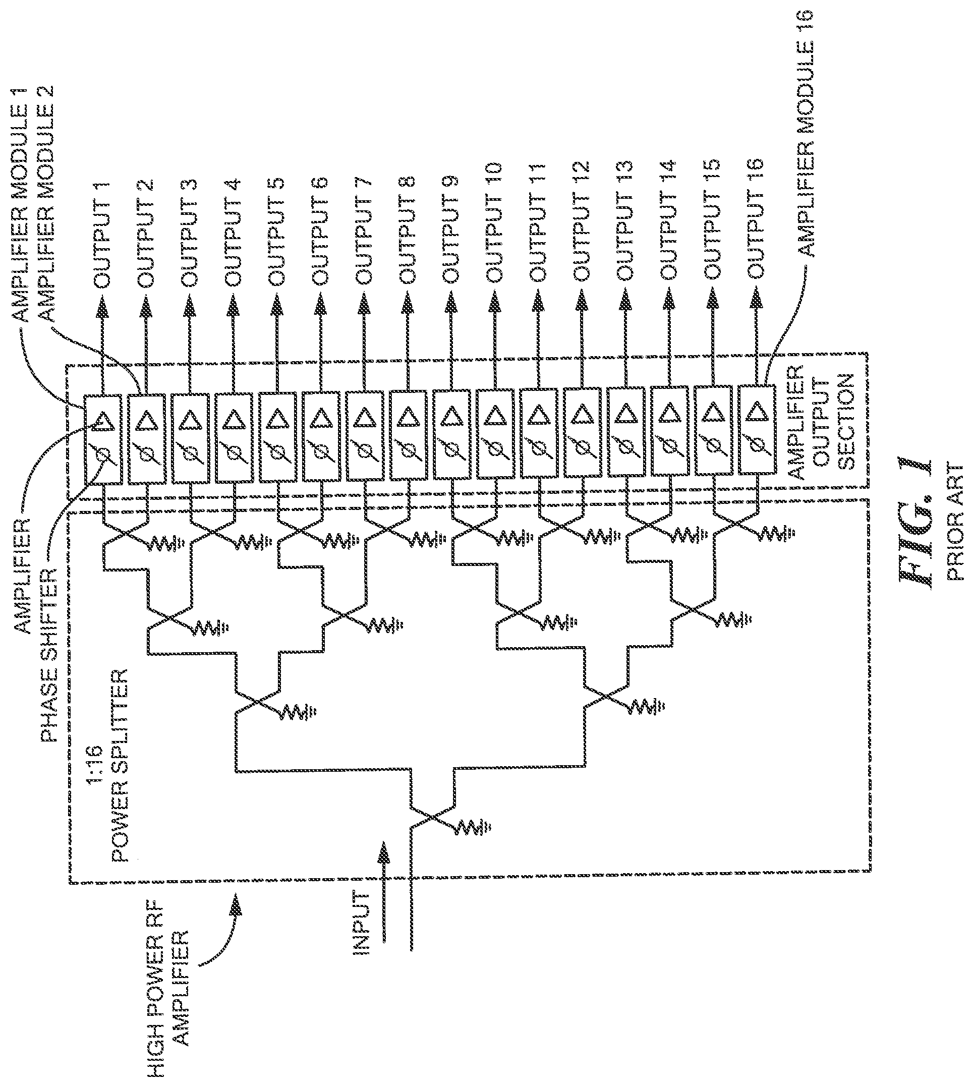
[0002] As is known in the art, many high power radio frequency (RF) amplifiers include a plurality of amplifier modules coupled to a common input through a power splitter; each one of the amplifier modules producing a corresponding one of a plurality of outputs. One such power amplifier is shown in FIG. 1, here in this example, having sixteen amplifier modules 1-16 producing outputs at a corresponding one of 16 outputs 1-16, as shown. The power RF amplifier includes a one to sixteen power splitter for dividing power of an RF signal at the input equally among the sixteen amplifier modules. Each one of the amplifier modules includes an adjustable phase shifter coupled between an output of a corresponding one of the power splitter and the input to such one of the amplifier modules, as shown. Since each one of the amplifier modules typically, when fabricated, will have a different phase shift through it, the phase shifters are adjusted during manufacture of the RF power amplifier so that the output signal from all of the sixteen amplifier modules are all in-phase with one another. That is, the signals at the outputs 1-16 are all in-phase. However, tuning each one of the plurality of phase shifters is time consuming.
SUMMARY OF THE INVENTION
[0003] In accordance with the present disclosure, a power amplifier is provided having; a plurality of N amplifiers, where N is an integer greater than one; an M:N power splitter having inputs, where M is an integer less than N, and N outputs, each one of the N outputs being coupled to an input of a corresponding one of the plurality of N amplifiers; and, a plurality of M delay lines, each one the M delay lines having an output coupled to a corresponding one of the M inputs of the plurality of the M:N power splitter, each one of the plurality of M delay lines being coupled to a common input of the power amplifier.
[0004] In one embodiment, the M:N power splitter and the M delay lines are disposed on a common printed circuit board.
[0005] In one embodiment, the amplifier includes a 1:M power splitter having M outputs, each one of the M outputs being coupled to an input of a corresponding one of the M delay lines.
[0006] In one embodiment, the N amplifiers are arranged in M amplifier module sections, each one of the M amplifier module sections having N/M of the amplifiers, each one of the N/M amplifiers in a corresponding one of the M amplifier module sections having a phase shift (.DELTA..sub.1+/-.delta.) degrees through (.DELTA..sub.M.+-./-.delta.) degrees, respectively, and where each one of the M delay lines has a phase shift .DELTA..sub.1 through .DELTA..sub.M respectively.
[0007] The details of one or more embodiments of the disclosure are set forth in the accompanying drawings and the description below. Other features, objects, and advantages of the disclosure will be apparent from the description and drawings, and from the claims.
BRIEF DESCRIPTION OF THE DRAWINGS
[0008] FIG. 1 is a schematic diagram of a high power RF power amplifier according to the PRIOR ART;
[0009] FIG. 2 is a is a schematic diagram of a high power RF power amplifier according to the disclosure; and
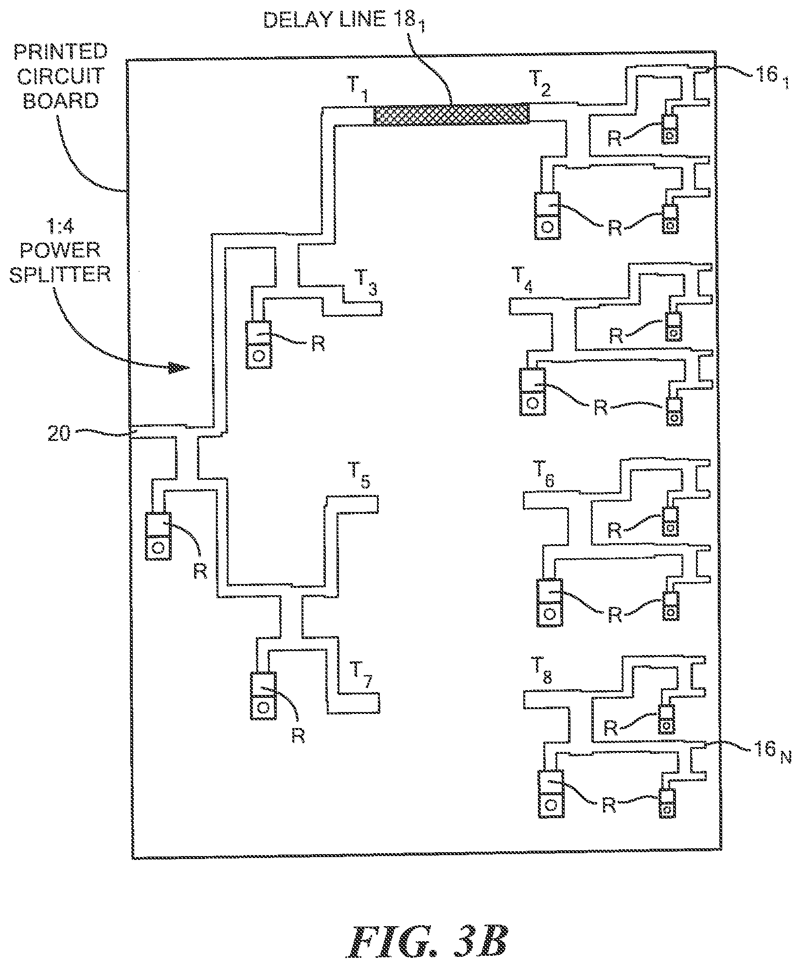
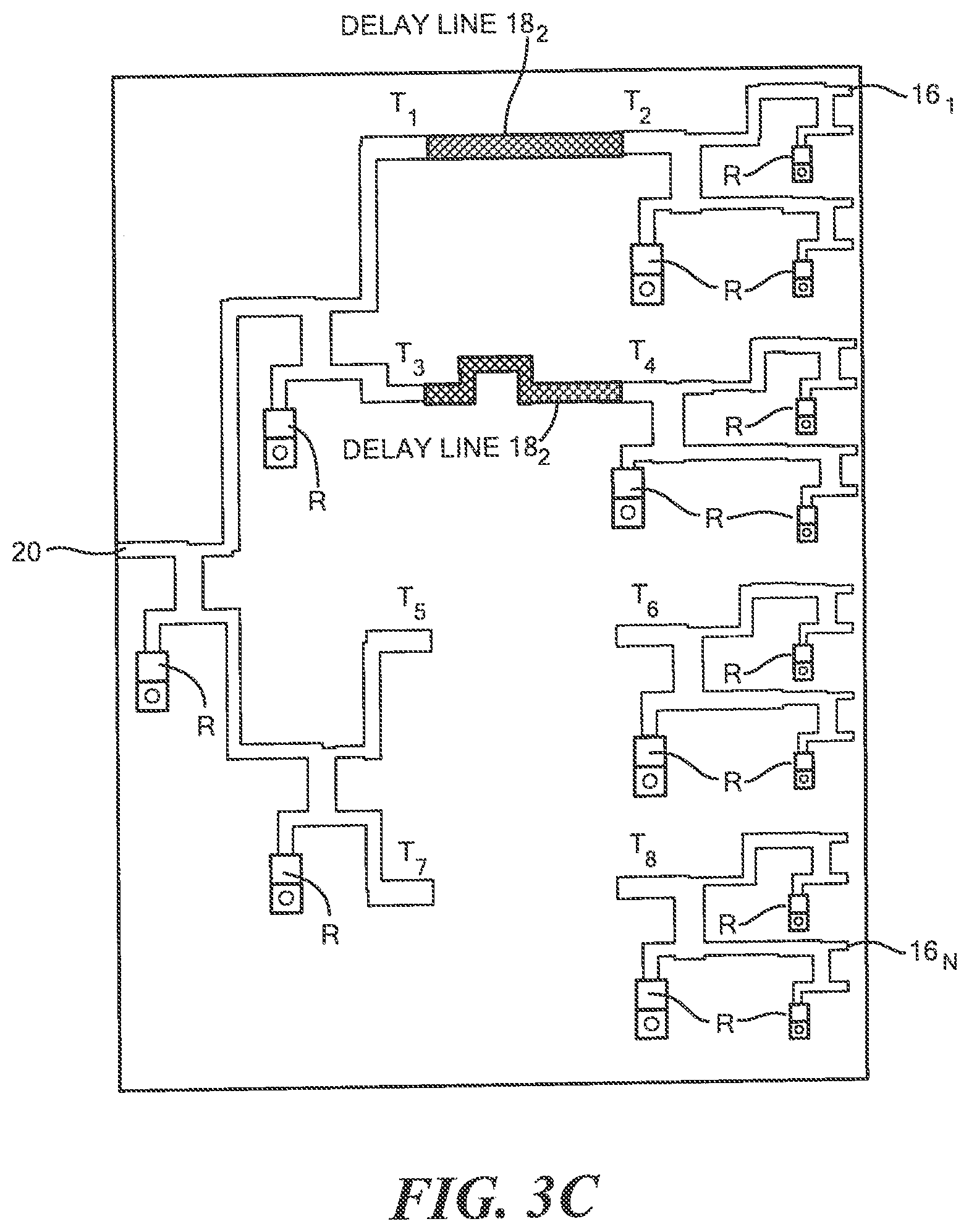
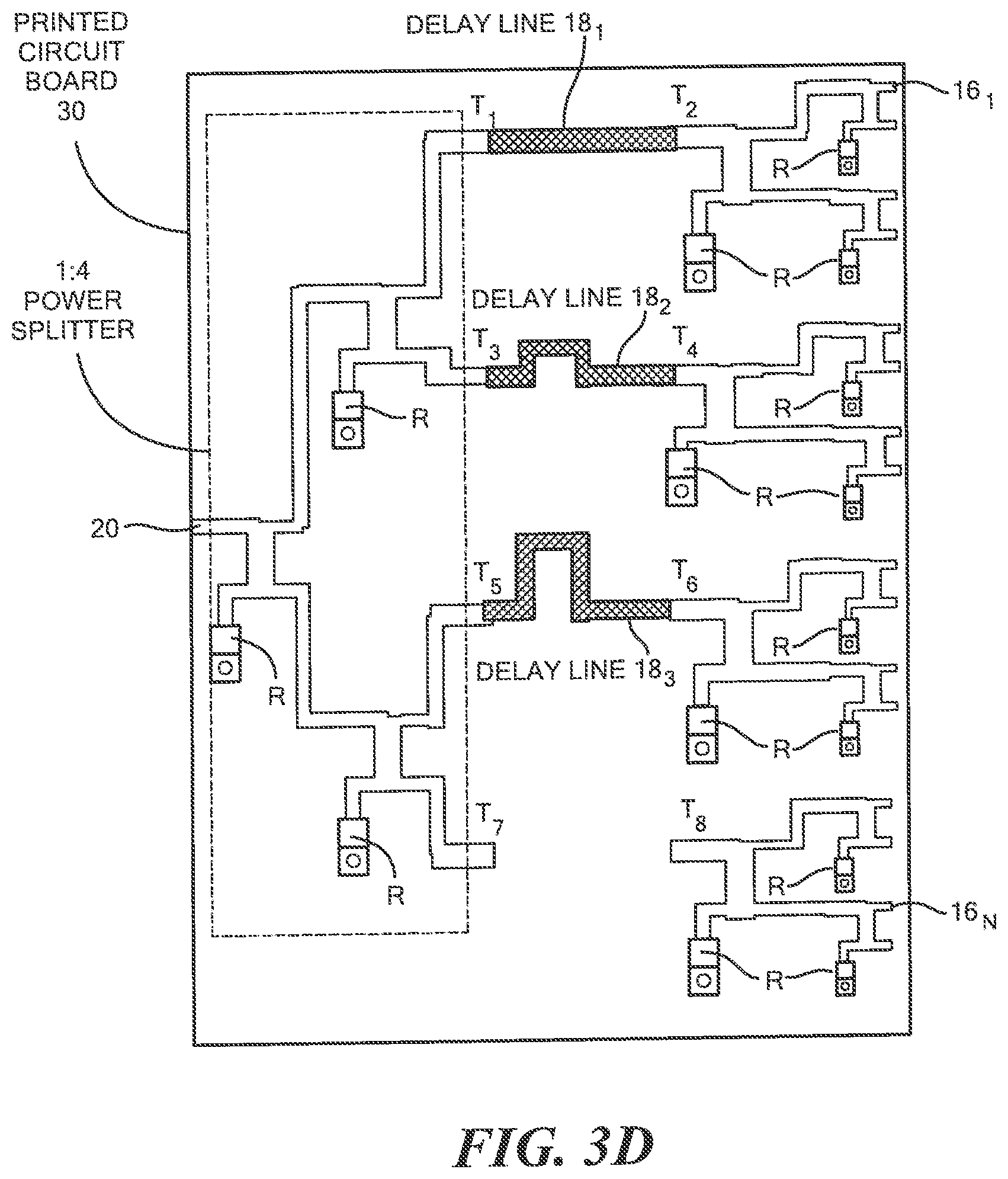
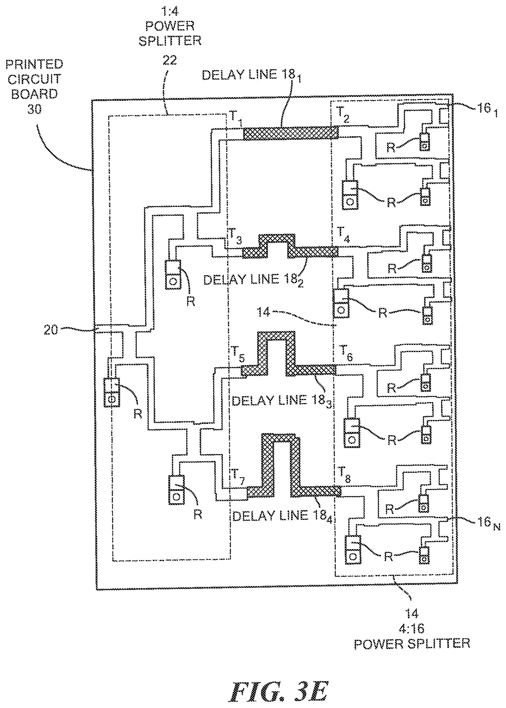
[0010] FIGS. 3A-3E are plan views of an upper surface of a printed circuit board having a 1:M power splitter, M:N power splitter, M delay lines 18.sub.1-18.sub.4, and resistors for use with the the high RF power amplifier of FIG. 2 at various stages in the fabrications thereof.
[0011] Like reference symbols in the various drawings indicate like elements.
DETAILED DESCRIPTION
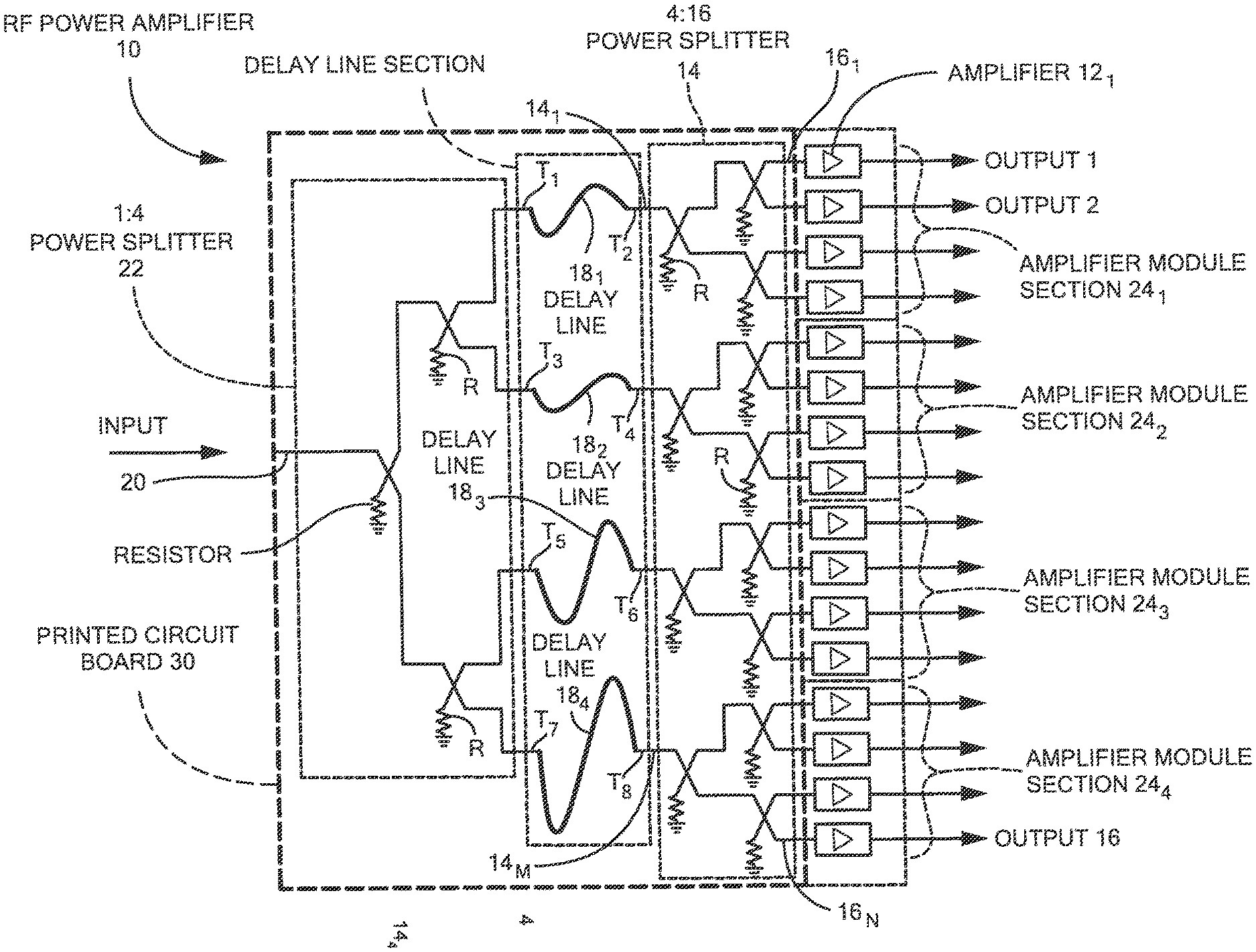
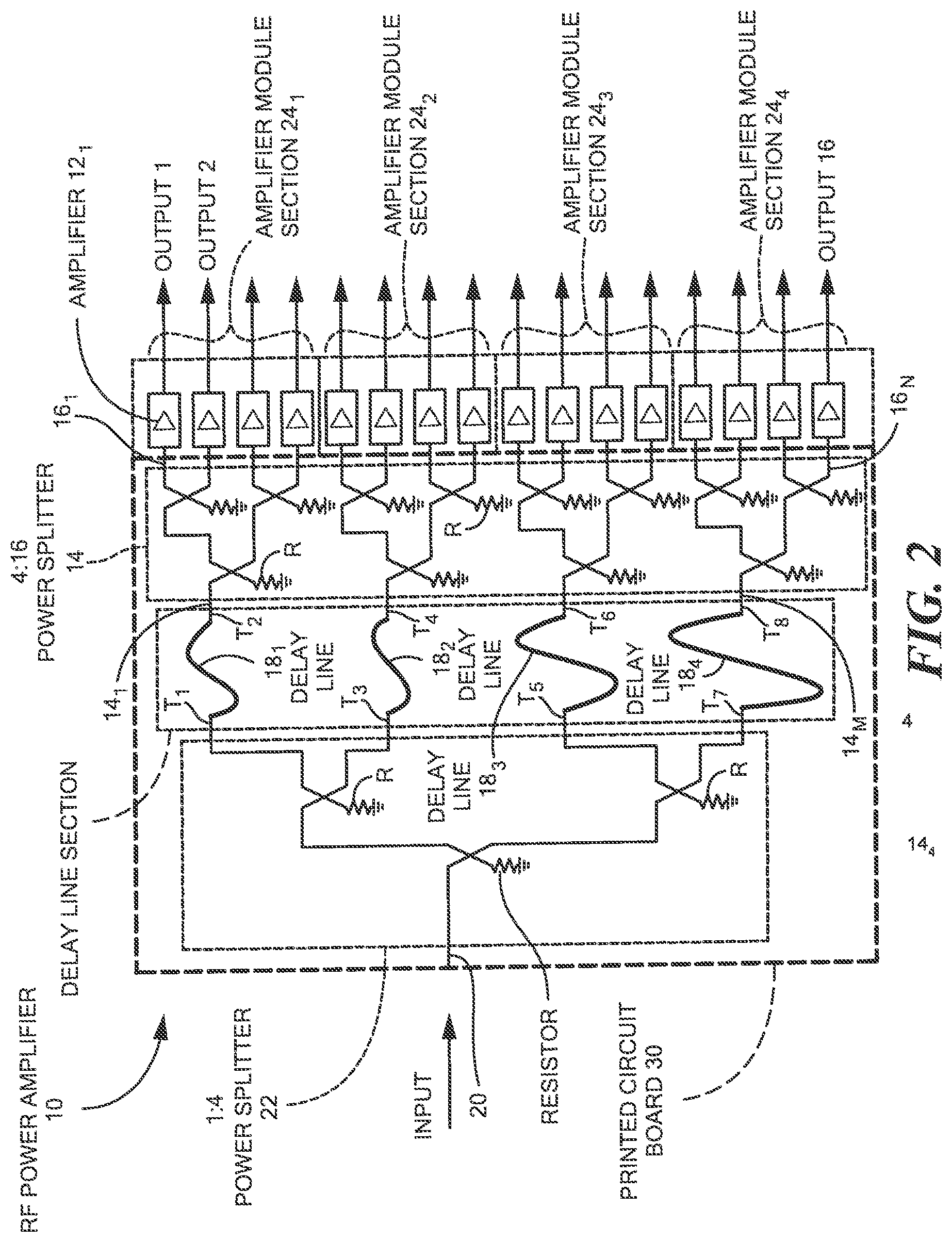
[0012] Referring now to FIG. 2, a high power RF amplifier 10 is shown having; a plurality of N amplifiers 12.sub.1-12.sub.N where N is an integer greater than one, here in this example N is sixteen; an M:N power splitter 14 having M inputs 14.sub.1-14.sub.M, where M is an integer less than N, here in this example, M is four, and N outputs 16.sub.1-16.sub.M, each one of the N outputs 16.sub.1-16.sub.M being coupled to an input 14.sub.1-14.sub.M of a corresponding one of the plurality of N amplifiers 12.sub.1-12.sub.N; and, a plurality of M delay lines 18.sub.1-18.sub.M, each one the M delay lines 18.sub.1-18.sub.M having an output T2, T4, T6, and T8, respectively, coupled to a corresponding one of the M inputs 14.sub.1-14.sub.M of the plurality of the M:N power splitter 14, each one of the plurality of M delay lines 18.sub.1-18.sub.M having an input T1, T3, T5 and T7, respectively, being coupled to a common input 20 of the power amplifier 10; here though a 1:N power splitter 22. It is noted that the 1:N power splitter and the M:N power splitter 14 are of conventional design and include conventional matched termination resistors R, here 50 ohms; the microwave transmission lines used to form the power splitters 14 and 22 as well as the and the delay lines 18.sub.1-18.sub.M here being in this example, 50 ohm microstrip transmission lines. Thus, there are, in this example, sixteen channels from the input 20 to a corresponding one of the sixteen outputs OUTPUT 1-OUTPUT 16.
[0013] Here, in this example, a plurality of amplifiers is fabricated and the phase shift through each one at the nominal operating frequently is measured and recorded. A predetermined tolerance +/-.delta. from a predetermined phase shift .DELTA..sub.1 through .DELTA..sub.M is selected for each one of the M amplifier module sections 24.sub.1-24.sub.M. Here for example, the predetermined tolerance .delta. is selected as five degrees and the predetermined phase shift .DELTA..sub.1 through .DELTA..sub.M are in this example selected as: .DELTA..sub.1=20 degrees, .DELTA..sub.1+10=30 degrees, .DELTA..sub.1+20=40 degrees and .DELTA..sub.1+30=50 degrees, for the M amplifier module sections 24.sub.1-24.sub.M respectively.
[0014] In this example, sixteen of the fabricated amplifiers are selected having the following phase shifts, in degrees: 16, 17, 22, 24, 26, 31, 34, 35, 36, 37, 42, 44, 48, 49, 52 and 53.
[0015] The selected amplifiers are arranged in the M amplifier module sections 24.sub.1-24.sub.M as follows:
TABLE-US-00001 Original Measured Target Phase Delay Line for Effective phase Phase Shift Shift per Amplifier (degrees) per Amplifier (Degrees) channel Module Section output channel Amplifier 12.sub.1 22 0 Degrees OUTPUT 1 = .+2 Module 12.sub.2 17 Amplifier Module OUTPUT 2 = -3 Section 12.sub.3 24 Section 24.sub.1 -20 OUTPUT 3 = +4 24.sub.1 12.sub.4 16 Degrees OUTPUT 4 = -4 Amplifier 12.sub.5 26 OUTPUT 5 = -4 Module 12.sub.6 31 Amplifier Module OUTPUT 6 = 1 Section 12.sub.7 34 Section 24.sub.2 -30 OUTPUT 7 = 4 24.sub.2 12.sub.8 35 Degrees OUTPUT 8 = 5 Amplifier 12.sub.9 36 OUTPUT 9 = 4 Module .sub. 12.sub.10 44 Amplifier Module OUTPUT 10 = 4 Section .sub. 12.sub.11 42 Section 24.sub.3 -40 OUTPUT 11 = 2 24.sub.3 .sub. 12.sub.12 37 Degrees OUTPUT 12 = -3 Amplifier .sub. 12.sub.13 48 OUTPUT 13 = -2 Module .sub. 12.sub.14 53 Amplifier Module OUTPUT 14 = 3 Section .sub. 12.sub.15 52 Section 24.sub.4 -50 OUTPUT 15 = -2 24.sub.4 .sub. 12.sub.16 49 Degrees OUTPUT 16 = -1
[0016] It is noted that the N amplifiers 12.sub.1-12.sub.16 are arranged in M amplifier module sections 24.sub.1-24.sub.M, each one of the M amplifier module sections 24.sub.1-24.sub.M having N/M (here 4) of the amplifiers 12.sub.1-12.sub.N, each one of the N/M amplifiers 12.sub.1-12.sub.N in a corresponding one of the M amplifier module sections 24.sub.1-24.sub.M having a phase shift (.DELTA..sub.1+/-.delta.) degrees through (.DELTA..sub.M+/-.delta.) degrees, respectively, and where each one of the M delay lines 18.sub.1-18.sub.M has a phase shift .DELTA..sub.1 through .DELTA..sub.M respectively.
[0017] It should be noted that the 1:M power splitter 22 and M:N power splitter 14 and the M delay lines 18.sub.1-18.sub.4 are disposed on a common printed circuit board 30 as microstrip microwave transmission lines and also formed on the printed circuit board 30 are the resistors R.
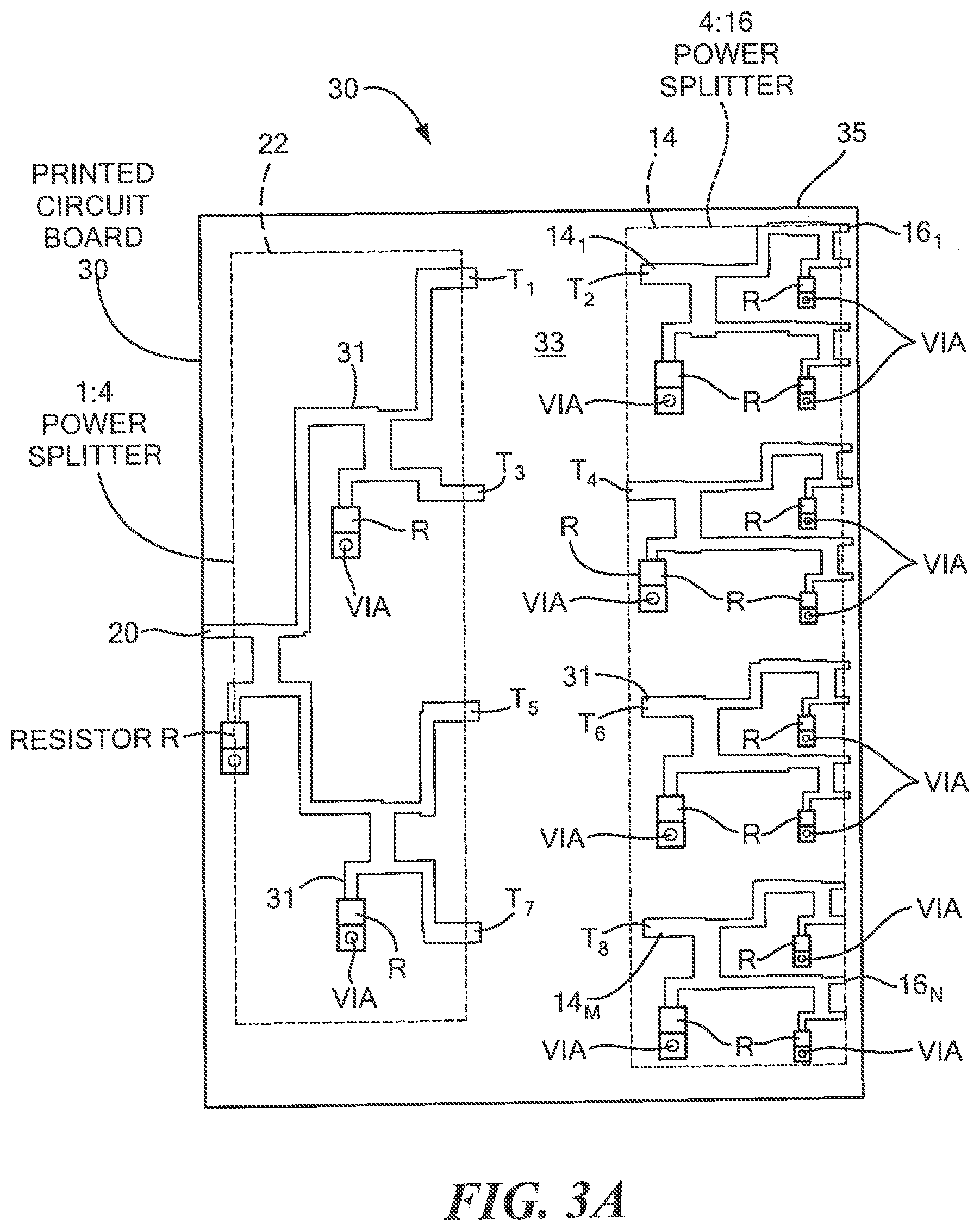
[0018] Referring now to FIGS. 3A-3E plan views of various stages in the fabrications of the printed circuit 30 portion of the high RF power amplifier 10 are shown. Thus, shows the 1:M power splitter 22, M:N power splitter 14 and the resistors R. Here the 1:M power splitter 22 and the M:N power splitter 14 are microstrip transmission lines formed by strip conductors 31 formed on the upper surface 33 of a dielectric board 35 and a ground plane conductor, not shown, formed on the bottom surface of the dielectric board 35. One end of the resistors R is connected to the strip conductors 31, as shown, and the other end of the resistors is connected to the ground plane conductor (not shown) through conductive vias VIA, as indicated.
[0019] After forming the printed circuit board 30 as in FIG. 3A, the delay lines 18.sub.1-18.sub.4 are formed as microstrip transmission lines; the ground plane being provided by the ground plane (not shown) formed on the back of the dielectric board 35. The strip conductor of the microstrip transmission line for the first delay line 18.sub.1 is printed using additive manufacturing or 3D printing as shown in FIG. 3B.
[0020] Next, the strip conductor of the microstrip transmission line for the second delay line 18.sub.2 is printed using additive manufacturing or 3D printing as shown in FIG. 3C.
[0021] Next the strip conductor of the microstrip transmission line for the third delay line 18.sub.3 is printed using additive manufacturing or 3D printing as shown in FIG. 3D.
[0022] Finally, the strip conductor of the microstrip transmission line for the fourth delay line 18.sub.4 is printed using additive manufacturing or 3D printing as shown in FIG. 3D.
[0023] It should be understood that while in the example above the strip conductors of the microstrip transmission line for delay lines 18.sub.1-18.sub.4 have been printed sequentially, they may be printed concurrently using for example a raster type motion for the 3D printing head.
[0024] A number of embodiments of the disclosure have been described. Nevertheless, it will be understood that various modifications may be made without departing from the spirit and scope of the disclosure. Accordingly, other embodiments are within the scope of the following claims.
* * * * *
D00000
D00001
D00002
D00003
D00004
D00005
D00006
D00007
XML
uspto.report is an independent third-party trademark research tool that is not affiliated, endorsed, or sponsored by the United States Patent and Trademark Office (USPTO) or any other governmental organization. The information provided by uspto.report is based on publicly available data at the time of writing and is intended for informational purposes only.
While we strive to provide accurate and up-to-date information, we do not guarantee the accuracy, completeness, reliability, or suitability of the information displayed on this site. The use of this site is at your own risk. Any reliance you place on such information is therefore strictly at your own risk.
All official trademark data, including owner information, should be verified by visiting the official USPTO website at www.uspto.gov. This site is not intended to replace professional legal advice and should not be used as a substitute for consulting with a legal professional who is knowledgeable about trademark law.