In-situ Growth Of Quantum Dots And Nano-crystals From One, Two, Or Three Dimensional Material
Thomas; Jayan ; et al.
U.S. patent application number 16/901245 was filed with the patent office on 2021-01-07 for in-situ growth of quantum dots and nano-crystals from one, two, or three dimensional material. This patent application is currently assigned to University of Central Florida Research Foundation, Inc.. The applicant listed for this patent is University of Central Florida Research Foundation, Inc.. Invention is credited to Farzana Chowdhury, Basudev Pradhan, Jayan Thomas.
| Application Number | 20210005831 16/901245 |
| Document ID | / |
| Family ID | |
| Filed Date | 2021-01-07 |


| United States Patent Application | 20210005831 |
| Kind Code | A1 |
| Thomas; Jayan ; et al. | January 7, 2021 |
IN-SITU GROWTH OF QUANTUM DOTS AND NANO-CRYSTALS FROM ONE, TWO, OR THREE DIMENSIONAL MATERIAL
Abstract
Techniques for growing, at least one of: (a) quantum dots and (b) nano-crystals, on a surface of a material are provided. One method comprises placing a precursor on the surface; adding an antisolvent to the precursor; and growing at least one of the quantum dots and the nanocrystals on the surface.
| Inventors: | Thomas; Jayan; (Orlando, FL) ; Pradhan; Basudev; (Kolkata, IN) ; Chowdhury; Farzana; (Orlando, FL) | ||||||||||
| Applicant: |
|
||||||||||
|---|---|---|---|---|---|---|---|---|---|---|---|
| Assignee: | University of Central Florida
Research Foundation, Inc. Orlando FL |
||||||||||
| Appl. No.: | 16/901245 | ||||||||||
| Filed: | June 15, 2020 |
Related U.S. Patent Documents
| Application Number | Filing Date | Patent Number | ||
|---|---|---|---|---|
| 62923074 | Oct 18, 2019 | |||
| 62869453 | Jul 1, 2019 | |||
| Current U.S. Class: | 1/1 |
| International Class: | H01L 51/42 20060101 H01L051/42; H01L 51/00 20060101 H01L051/00 |
Goverment Interests
U.S. GOVERNMENT LICENSE RIGHTS
[0002] This invention was made with Government support under Award No. 1351757 awarded by NSF. The Government has certain rights in the invention.
Claims
1. A method of growing, at least one of: (a) quantum dots and (b) nano-crystals, on a surface of a material, the method comprising: placing a precursor on the surface; adding an antisolvent to the precursor; and growing on the surface the at least one of quantum dots and nano-crystals.
2. The method of claim 1, further comprising activating the surface.
3. The method of claim 1, further comprising removing remaining precursor.
4. The method of claim 2, wherein activating the surface comprises performing dry or wet etching of the surface.
5. The method of claim 1, wherein the at least one of: (a) quantum dots and (b) nano-crystals are separated from the surface of the material by a minimum distance.
6. The method of claim 5, wherein the minimum distance is less than 0.5 nm.
7. The method of claim 1, wherein the at least one of: (a) quantum dots and (b) nano-crystals consists of perovskite quantum dots; and wherein the precursor is a perovskite precursor.
8. The method of claim 1, wherein the material comprises graphene, carbon nanotubes, or at least one doped semiconductor.
9. The method of claim 1, wherein the carrier mobility of the material is higher than the carrier mobility of the at least one of: (a) quantum dots and (b) nano-crystals.
10. The method of claim 1, wherein the antisolvent comprises at least one of toluene, diethyl ether, chlorobenzene, and chloroform.
11. A device, comprising: a material having a surface; at least one of (a) quantum dots and (b) nano-crystals grown on the surface of the material; and wherein the at least one of: (a) quantum dots and (b) nano-crystals are separated from the surface of the material by a minimum distance.
12. The device of claim 11, wherein the surface has been activated creating more defects on the surface.
13. The device of claim 11, wherein the minimum distance is less than 0.5 nm.
14. The device of claim 11, wherein the at least one of (a) quantum dots and (b) nano-crystals consists of perovskite quantum dots.
15. The device of claim 11, wherein the material comprises graphene, carbon nanotubes, or at least one doped semiconductor.
16. The device of claim 11, wherein the carrier mobility of the material is higher than the carrier mobility of the at least one of: (a) quantum dots and (b) nano-crystals.
17. A device, comprising: graphene having a surface; at least one of: (a) quantum dots and (b) nano-crystals grown on the surface of the graphene; wherein the at least one of: (a) quantum dots and (b) nano-crystals are separated from the surface of the graphene by a minimum distance; wherein the carrier mobility of the graphene is higher than the carrier mobility of the at least one of: (a) quantum dots and (b) nano-crystals; and wherein the device is configured to be used in a photonic device.
18. The device of claim 17, wherein the graphene is two dimensional single layer graphene.
19. The device of claim 17, wherein the minimum distance is less than 0.5 nm.
20. The device of claim 17, wherein the at least one of (a) quantum dots and (b) nano-crystals consists of perovskite quantum dots.
Description
CROSS-REFERENCE TO RELATED APPLICATIONS
[0001] The present application claims benefit of U.S. Patent Application Ser. No. 62/869,453 filed Jul. 1, 2019 and U.S. Patent Application Ser. No. 62/923,074 filed Oct. 18, 2019; the entire contents of the aforementioned patent applications are incorporated herein by reference as if set forth in their entirety.
BACKGROUND
[0003] Phototransistors have been made by depositing pre-formed organic-inorganic halide perovskite quantum dots (PQDs) to graphene. The PQDs were deposited by spin coating a solution of PQDs on the graphene. The PQDs are formed by homogeneous nucleation.
[0004] PQDs have high absorption coefficients and high photogeneration efficiency which make them desirable for use in phototransistors. However, PQDs have a low carrier mobility which is undesirable for optoelectronic devices. Because graphene has a high carrier mobility, the structure resulting from depositing PQDs on the graphene has an increased carrier mobility than the carrier mobility of the PQDs. Further, the resulting structure retains the high absorption coefficient and high electron-hole diffusion length of the PQDs.
[0005] As a result, a device using the structure has increased photoresponsivity which is desirable, e.g., for a phototransistor. However, because the PQDs are deposited on the graphene, the resulting separation between the PQDs and graphene limits carrier mobility, and thus the photoresponsivity of the structure.
SUMMARY
[0006] A method of growing, at least one of: (a) quantum dots and (b) nano-crystals, on a surface of a material is provided. The method comprises placing a precursor on the surface; adding an antisolvent to the precursor; and growing at least one of the quantum dots and the nanocrystals on the surface.
DRAWINGS
[0007] Embodiments of the present invention can be more easily understood and further advantages and uses thereof more readily apparent, when considered in view of the description of the preferred embodiments and the following figures in which:
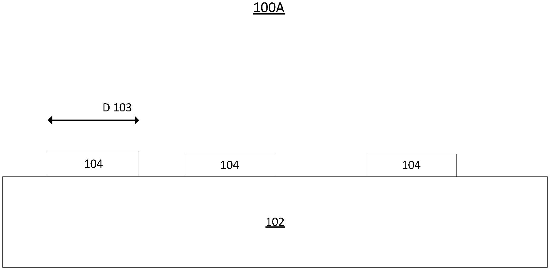
[0008] FIG. 1A illustrates one embodiment of a structure formed by QDs grown from a material; and
[0009] FIG. 1B is a flow diagram illustrating one embodiment of a method for forming a quantum dot from a material.
[0010] In accordance with common practice, the various described features are not drawn to scale but are drawn to emphasize features relevant to the present invention. Reference characters denote like elements throughout figures and text.
DETAILED DESCRIPTION
[0011] In the following detailed description, reference is made to the accompanying drawings that form a part hereof, and in which is shown by way of specific illustrative embodiments in which the invention may be practiced. These embodiments are described in sufficient detail to enable those skilled in the art to practice the invention, and it is to be understood that other embodiments may be utilized and that logical, mechanical and electrical changes may be made without departing from the scope of the present invention. The following detailed description is, therefore, not to be taken in a limiting sense.
[0012] Embodiments of the invention are applicable to quantum dots (QDs) and nano-crystals. Nano-crystals have a larger diameter than quantum dots and have growth times longer than quantum dots. For pedagogical purposes embodiments of the invention will be subsequently described with reference solely to quantum dots, but is also applicable to nanocrystals.
[0013] Quantum dots may be grown, e.g., by heterogeneous nucleation, from one, two, or three dimensional material. Optionally, grown from material means grown on material. The material may have one or more properties (but not limited to) such as high carrier mobility, high carrier density ultrafast charge separation, fast charge transfer between QDs and the material, and/or better plasmonic field enhancement.
[0014] In situ growth of QDs on the material results in a structure having a least or minimum distance between the QDs and a surface of the material upon which they are grown. For example, the distance between the QDs and the material may be less than 0.5 nm; however, this distance may vary based upon materials and methods used to grow the QDs on the material. By being more closely co-located with the material, charge transfer from the QDs to such material is increased.
[0015] As a result, the structure formed by growing QDs on the material (structure) not only retains the large absorption coefficient and photogeneration efficiency of the QDs, but also provides the properties of the substrate. The properties of the structure are closer to the properties of the material from which this structure is formed. For example, electron mobility of the structure may be nearly equal to 2500 cm.sup.2V.sup.-1s.sup.-1 if such material having high carrier mobility are two dimensional single graphene layers.
[0016] As a result, photonic devices (e.g., photodiodes and phototransistors) made with the structures formed by growing QDs on material have increased photoresponsivity than devices formed by depositing QDs to such material. For example, the structure can form all or part of a base of a bipolar junction phototransistor or of a gate of a field effect phototransistor. Photoresponsivity greater than 10.sup.8 AW.sup.-1 have been measured for field effect phototransistors including PQDs grown on graphene which is about three orders of magnitude higher than the photoresponsivity of photonic devices made QDs, such as PQDs, deposited on graphene.
[0017] Material means any one, two, or three dimensional material having some unique properties, e.g., as discussed above. Materials include without limitation graphene, carbon nanotubes, and doped semiconductors (including without limitation heterojunctions). Further, the QDs may be PQDs and/or other types of QDs. Other types of QDs can be made from binary compounds such as lead sulfide, lead selenide, cadmium selenide, cadmium sulfide, cadmium telluride, indium arsenide, and indium phosphide.
[0018] The frequency response of QDs is dependent upon QD diameter; as QD diameter increases the frequencies detected by the QDs increases. In some embodiments, QD diameter may fall within a range of 2-6 nm in diameter; however, QD diameter range may differ in other embodiments. QD diameter is a function of the amount of time a QD is grown, e.g., using the exemplary methods described below.
[0019] FIG. 1A illustrates one embodiment of a structure 100A formed by QDs grown from a material. The structure comprises QDs 104 grown on the material 102. The QDs have a diameter, D, 103
[0020] An exemplary method of manufacturing QDs grown on such material will now be described. FIG. 1B is a flow diagram illustrating one embodiment of a method 100B for forming a quantum dot on from a material. The blocks of the flow diagram have been arranged in a generally sequential manner for ease of explanation; however, it is to be understood that this arrangement is merely exemplary, and it should be recognized that the processing associated with the methods (and the blocks shown in the Figures) can occur in a different order (for example, where at least some of the processing associated with the blocks is performed in parallel and/or in an event-driven manner).
[0021] Optionally, in block 102, activate a surface, of the material, upon which QDs are to be grown. Surface activation creates more defects in the material. By increasing the number of defects on the surface of such material, density and coverage of QDs grown on the material is increased. The defects can be created for example by dry or wet chemistry. For example, surface activation can be performed by plasma etching the surface with a plasma etcher.
[0022] In some embodiments, the material having high carrier mobility is already formed as a portion of a photonic device. For example, the material having high carrier mobility may already form a portion of a base of a bipolar phototransistor or form part of a region over a channel of a field effect phototransistor.
[0023] In block 105, place a precursor on the surface. The precursor may be deposited on the surface of the material. For example, if PQDs are to be formed, then a perovskite precursor is used. The perovskite precursor may be prepared with ligand assisted re-precipitation (LARP) by mixing stoichiometric ratios of lead bromide (PbBr.sub.2) and methyl ammonium bromide (CH.sub.3NH.sub.3Br) salts in a solvent like dimethylformamide (DMF). Then, ligands of butylamine and oleic acid are added to form the perovskite precursor solution; optionally sonification may be used when adding the ligands to hasten the mixing process. Note, other precursors can be used, e.g., that do not use perovskite material or which do not use LARP; for example, lead and sulfur precursors may be deposited on the surface of the material to grow lead sulfide quantum dots.
[0024] In block 106, adding an antisolvent into the precursor. The antisolvent may be deposited into the precursor or vice versa. The antisolvent makes the precursor less soluble and forms droplets of precursor in the antisolvent. The antisolvent may be toluene, diethyl ether, chlorobenzene, chloroform, and/or another chemical that is an antisolvent.
[0025] In block 108, grow QDs on the surface. The droplets of the precursor precipitate seeding (or crystallization) of embryo(s) when a droplet is located at active and/or defect site(s) on the surface of the material having high carrier mobility. The active sites have energies which are sufficiently high to cause heterogeneous nucleation of the QDs at each active site. Defect sites are a type of an active site. Optionally, blocks 102, 104, 106, and/or 108 may be performed at a temperature in a range between 0 C and 150 C.
[0026] A QD is formed from an embryo only if the embryo diameter (or corresponding energy) grows to exceed a critical diameter (or critical energy). Such QD growth rate and surface density can be increased by increasing the temperature of the surface of the material having high mobility; this is because the number of active sites is increased on the surface when increasing the temperature of the surface. The critical diameter, and critical energy, depends upon the type of material used to form the QDs.
[0027] In block 110, optionally, remove remaining precursor, e.g., on the surface. The remaining precursor can be removed by washing the material on which QDs are grown, e.g., with an antisolvent or a solvent. However, the precursor may be removed by other techniques.
EXEMPLARY EMBODIMENTS
[0028] Example 1 includes a method of growing, at least one of: (a) quantum dots and (b) nano-crystals, on a surface of a material, the method comprising: placing a precursor on the surface; adding an antisolvent to the precursor; and growing on the surface the at least one of quantum dots and nano-crystals.
[0029] Example 2 includes the method of Example 1, further comprising activating the surface.
[0030] Example 3 includes the method of any of Examples 1-2, further comprising removing remaining precursor.
[0031] Example 4 includes the method of any of Examples 2-3, wherein activating the surface comprises performing dry or wet etching of the surface.
[0032] Example 5 includes the method of any of Examples 1-4, wherein the at least one of: (a) quantum dots and (b) nano-crystals are separated from the surface of the material by a minimum distance.
[0033] Example 6 includes the method of Example 5, wherein the minimum distance is less than any of Examples 0-1.5 nm.
[0034] Example 7 includes the method of any of Examples 1-6, wherein the at least one of: (a) quantum dots and (b) nano-crystals consists of perovskite quantum dots; and wherein the precursor is a perovskite precursor.
[0035] Example 8 includes the method of any of Examples 1-7, wherein the material comprises graphene, carbon nanotubes, or at least one doped semiconductor.
[0036] Example 9 includes the method of any of Examples 1-8, wherein the carrier mobility of the material is higher than the carrier mobility of the at least one of: (a) quantum dots and (b) nano-crystals.
[0037] Example 10 includes the method of any of Examples 1-8, wherein the antisolvent comprises at least one of toluene, diethyl ether, chlorobenzene, and chloroform.
[0038] Example 11 includes a device, comprising: a material having a surface; at least one of (a) quantum dots and (b) nano-crystals grown on the surface of the material; and wherein the at least one of: (a) quantum dots and (b) nano-crystals are separated from the surface of the material by a minimum distance.
[0039] Example 12 includes the device of Example 11, wherein the surface has been activated creating more defects on the surface.
[0040] Example 13 includes the device of any of Examples 11-13, wherein the minimum distance is less than any of Examples 0-1.5 nm.
[0041] Example 14 includes the device of any of Examples 11-13, wherein the at least one of (a) quantum dots and (b) nano-crystals consists of perovskite quantum dots.
[0042] Example 15 includes the device of any of Examples 11-14, wherein the material comprises graphene, carbon nanotubes, or at least one doped semiconductor.
[0043] Example 16 includes the device of any of Examples 11-15, wherein the carrier mobility of the material is higher than the carrier mobility of the at least one of: (a) quantum dots and (b) nano-crystals.
[0044] Example 17 includes a device, comprising: graphene having a surface; at least one of: (a) quantum dots and (b) nano-crystals grown on the surface of the graphene; wherein the at least one of: (a) quantum dots and (b) nano-crystals are separated from the surface of the graphene by a minimum distance; wherein the carrier mobility of the graphene is higher than the carrier mobility of the at least one of: (a) quantum dots and (b) nano-crystals; and wherein the device is configured to be used in a photonic device.
[0045] Example 18 includes the device of Example 17, wherein the graphene is two dimensional single layer graphene.
[0046] Example 19 includes the device of any of Examples 17-18, wherein the minimum distance is less than any of Examples 0-1.5 nm.
[0047] Example 20 includes the device of any of Examples 17-19, wherein the at least one of (a) quantum dots and (b) nano-crystals consists of perovskite quantum dots
[0048] Terms of relative position as used in this application are defined based on a plane parallel to the conventional plane or working surface of a material (e.g., a layer or a substrate), regardless of orientation. Terms such as "on," "higher," "lower," "over," "top," and "under" are defined with respect to the conventional plane or working surface being on the top surface of a layer or substrate, regardless of orientation.
[0049] Although specific embodiments have been illustrated and described herein, it will be appreciated by those of ordinary skill in the art that any arrangement, which is calculated to achieve the same purpose, may be substituted for the specific embodiment shown. This application is intended to cover any adaptations or variations of the present invention. Therefore, it is manifestly intended that this invention be limited only by the claims and the equivalents thereof.
* * * * *
D00000
D00001
D00002
XML
uspto.report is an independent third-party trademark research tool that is not affiliated, endorsed, or sponsored by the United States Patent and Trademark Office (USPTO) or any other governmental organization. The information provided by uspto.report is based on publicly available data at the time of writing and is intended for informational purposes only.
While we strive to provide accurate and up-to-date information, we do not guarantee the accuracy, completeness, reliability, or suitability of the information displayed on this site. The use of this site is at your own risk. Any reliance you place on such information is therefore strictly at your own risk.
All official trademark data, including owner information, should be verified by visiting the official USPTO website at www.uspto.gov. This site is not intended to replace professional legal advice and should not be used as a substitute for consulting with a legal professional who is knowledgeable about trademark law.