Scintillator Radiation Detector And Corresponding Dosimeter
LOI; Sara ; et al.
U.S. patent application number 16/917517 was filed with the patent office on 2021-01-07 for scintillator radiation detector and corresponding dosimeter. The applicant listed for this patent is STMICROELECTRONICS S.r.l.. Invention is credited to Paolo CREMA, Alessandro FREGUGLIA, Sara LOI.
| Application Number | 20210003721 16/917517 |
| Document ID | / |
| Family ID | |
| Filed Date | 2021-01-07 |


| United States Patent Application | 20210003721 |
| Kind Code | A1 |
| LOI; Sara ; et al. | January 7, 2021 |
SCINTILLATOR RADIATION DETECTOR AND CORRESPONDING DOSIMETER
Abstract
A device such as a dosimeter for detecting ionizing radiation, for example, X-ray radiation, in hospitals or the like. The device includes scintillator material configured to produce light as a result of radiation interacting with the scintillator material, and photoelectric conversion circuitry optically coupled to the scintillator material and configured to produce electrical signals via photoelectric conversion of light produced by the scintillator material. The device includes a plurality of photoelectric converters optically coupled with the scintillator material at spatially separated locations. The plurality of photoelectric converters thus produce respective electrical signals by photoelectric conversion of light produced by the scintillator material as a result of radiation interacting with the scintillator material. Improved energy linearity is thus facilitated while providing more efficient detection over the whole energy spectrum of radiation detected.
| Inventors: | LOI; Sara; (Villaputzu, IT) ; CREMA; Paolo; (Vimercate, IT) ; FREGUGLIA; Alessandro; (Milano, IT) | ||||||||||
| Applicant: |
|
||||||||||
|---|---|---|---|---|---|---|---|---|---|---|---|
| Appl. No.: | 16/917517 | ||||||||||
| Filed: | June 30, 2020 |
| Current U.S. Class: | 1/1 |
| International Class: | G01T 1/20 20060101 G01T001/20; G01T 1/02 20060101 G01T001/02 |
Foreign Application Data
| Date | Code | Application Number |
|---|---|---|
| Jul 2, 2019 | IT | 102019000010638 |
Claims
1. A device, comprising: a scintillator material; and photoelectric conversion circuitry optically coupled to the scintillator material, the photoelectric conversion circuitry including a plurality of photoelectric converters that are optically coupled with the scintillator material at different portions of the scintillator material.
2. The device of claim 1, wherein the scintillator material includes at least one scintillator body extending in a first direction, and wherein a first photoelectric converter and a second photoelectric converter of the plurality of photoelectric converters are coupled with the at least one scintillator body at locations spatially separated along the first direction.
3. The device of claim 1, wherein the plurality of photoelectric converters comprise: at least one first photoelectric converter coupled with the scintillator material at a first surface of the scintillator material; and at least one second photoelectric converter coupled with the scintillator material at a second surface of the scintillator material that is different from the first surface.
4. The device of claim 1, wherein the scintillator material includes a plurality of portions, each of the plurality of portions optically coupled to at least one respective photoelectric converter of the plurality of photoelectric converters.
5. The device of claim 4, wherein a first portion and a second portion of the plurality of portions of the scintillator material have different dimensions from one another.
6. The device of claim 4, wherein a first portion and a second portion of the plurality of portions of the scintillator material have different materials from one another.
7. The device of claim 4, wherein the plurality of portions of the scintillator material are juxtaposed to one another.
8. The device of claim 1, wherein the plurality of photoelectric converters include one or more silicon photomultipliers or one or more arrays of single-photon avalanche diodes.
9. The device of claim 1, comprising a casing of photon-reflective material surrounding the scintillator material and the plurality of photoelectric converters.
10. The device of claim 1, comprising: a substrate under the scintillator material and the plurality of photoelectric converters; and signal processing circuitry coupled to the plurality of photoelectric converters and configured to process the electrical signals produced by the photoelectric conversion circuitry.
11. The device of claim 1, wherein the scintillator material is configured to produce light upon receiving radiation that interacts with the scintillator material; and wherein the photoelectric conversion circuitry is configured to produce electrical signals via photoelectric conversion of the light produced by the scintillator material
12. A dosimeter, comprising: a first scintillator body having a first surface arranged to receive ionizing radiation, a second surface opposite to the first surface, and at least one third surface that meets both the first surface and the second surface; and at least one photoelectric converter optically coupled to the at least one third surface of the first scintillator body.
13. The dosimeter of claim 12, wherein the at least one photoelectric converter includes a first photoelectric converter and a second photoelectric converter coupled to a same third surface of the at least one third surface, the first photoelectric converter aligned with the second photoelectric converter in a direction between the first surface and the second surface of the first scintillator body.
14. The dosimeter of claim 13, wherein each of the first photoelectric converter and the second photoelectric converter is coupled to three third surfaces of the at least one third surface of the first scintillator body.
15. The dosimeter of claim 12, wherein the at least one photoelectric converter is physically spaced apart from the at least one third surface of the first scintillator body.
16. The dosimeter of claim 12, comprising at least one photoelectric converter coupled to the second surface of the first scintillator body.
17. The dosimeter of claim 16, wherein the at least one photoelectric converter coupled to the second surface of the scintillator body includes a third photoelectric converter that is optically coupled to the at least one third surface of the first scintillator body.
18. The dosimeter of claim 17, wherein the second scintillator body has a fourth surface adjacent to the sensing surface, a first distance between the first surface of the first scintillator body and the sensing surface being different than a second distance between the fourth surface of the second scintillator body and the sensing surface.
19. A device, comprising: a substrate; a first scintillator body over the substrate and having a first surface and a second surface opposite to the first surface, the first surface being proximal to the substrate and the second surface being distal to the substrate; and a second scintillator body over the substrate and having a third surface and a fourth surface opposite to the third surface, the third surface being proximal to the substrate and the fourth surface being distal to the substrate, the fourth surface being further away from the substrate than the second surface.
20. The device of claim 19, comprising a first photoelectric converter coupled to the first scintillator body and a second photoelectric converter coupled to the second scintillator body.
Description
BACKGROUND
Technical Field
[0001] The description relates to scintillator devices.
Description of the Related Art
[0002] Dosimeters are devices capable of detecting ionizing radiation (X rays, for instance).
[0003] Dosimeters are currently manufactured, for instance, using thermo-luminescence devices (TLD), which are however affected by an intrinsic drawback related to reading operations which involve operator intervention, which may be expensive and turn out to be time-consuming.
[0004] Application of those devices may thus be limited to measurements averaged over time and can hardly be proposed for real time measurements.
[0005] Being able to provide electronic, solid-state detectors capable of operating as radiation dosimeters would be a desirable goal to pursue, also in view of possible applications in an Internet-of-Things (IoT) context. In that context, real time measurements would, for instance, facilitate activating warnings as a result of high dose or dose rate values being reached, without waiting for completion of the integration time of the measurement and the time for reading operations.
[0006] Scintillator materials/devices can be considered for such applications in view of their capability of facilitating indirect conversion of radiation into electric charge. Scintillator materials/devices are capable of producing, as a result of interaction with radiation propagating through the scintillator material, light (that is photons) which can be eventually converted into electrical charge, and thus electrical signals, via photoelectric converters. Photodetectors such as silicon photomultipliers (SiPMs) may be exemplary of such photoelectric converters.
[0007] Scintillator-based dosimeters look promising in comparison with other electronic solutions such as hybrid direct-ion storage devices which are sometimes used for high-end applications and tend to be quite expensive.
[0008] Applying scintillator materials/devices to dosimetry is however adversely affected by at least two factors: [0009] possible different depths of propagation of the radiation within a scintillator material (as a function of a different energy of the radiation) may militate against energy linearity, that is the capability of providing output signals having a substantially linear dependency on the radiation energy; and [0010] variable detection efficiency over the whole energy spectrum of the radiation detected.
BRIEF SUMMARY
[0011] One or more embodiments may be applied, for instance, in "smart" dosimeters for radiation protection (for instance, against X rays) in hospitals and other installations or in RX detectors in equipment for diagnostics in medicine.
[0012] One or more embodiments may relate to a corresponding dosimeter.
[0013] One or more embodiments may provide a device for radiation dosimetry which is compatible with an Internet-of-Things (IoT) approach.
[0014] One or more embodiments may comprise photoelectric converters (silicon photomultipliers or SiPMs, for instance) assembled with scintillator material placed "on top" of them.
[0015] One or more embodiments may provide different approaches in order to improve, for instance, energy linearity and detection efficiency.
[0016] For instance, a matrix of photoelectric detectors (SiPMs, for instance) can be placed on the vertical walls of a body of scintillator material with the capability of measuring the depth of interaction of radiation in the scintillator. In that way, a correction factor can be calculated for geometrical efficiency by taking into account the relationship to the radiation energy.
[0017] Also, a parallel detection chain with optimized scintillator thickness or material (with step-wise or continuous thickness variation, for instance) can be provided, for instance, in order to improve detection efficiency in the energy spectrum.
BRIEF DESCRIPTION OF THE SEVERAL VIEWS OF THE DRAWINGS
[0018] One or more embodiments will now be described, by way of example only, with reference to the figures, wherein:
[0019] FIG. 1 is a perspective view of a conventional scintillator arrangement,
[0020] FIG. 2 is a perspective view of a device according to embodiments as described herein,
[0021] FIG. 3 is a cross-sectional view of a device as shown in FIG. 2,
[0022] FIG. 4 is a partial plan view in a direction corresponding to line IV of FIG. 3, and
[0023] FIG. 5 is a perspective view of a device according to embodiments as described herein.
DETAILED DESCRIPTION
[0024] In the ensuing description one or more specific details are illustrated, aimed at providing an in-depth understanding of examples of embodiments. The embodiments may be obtained without one or more of the specific details, or with other methods, components, materials, etc. In other cases, known structures, materials, or operations are not illustrated or described in detail so that certain aspects of embodiments will not be obscured.
[0025] Reference to "an embodiment" or "one embodiment" in the framework of the present description is intended to indicate that a particular configuration, structure, or characteristic described in relation to the embodiment is comprised in at least one embodiment. Hence, phrases such as "in an embodiment" or "in one embodiment" that may be present in one or more points of the present description do not necessarily refer to one and the same embodiment. Moreover, particular conformations, structures, or materials or other characteristics may be combined in any adequate way in one or more embodiments.
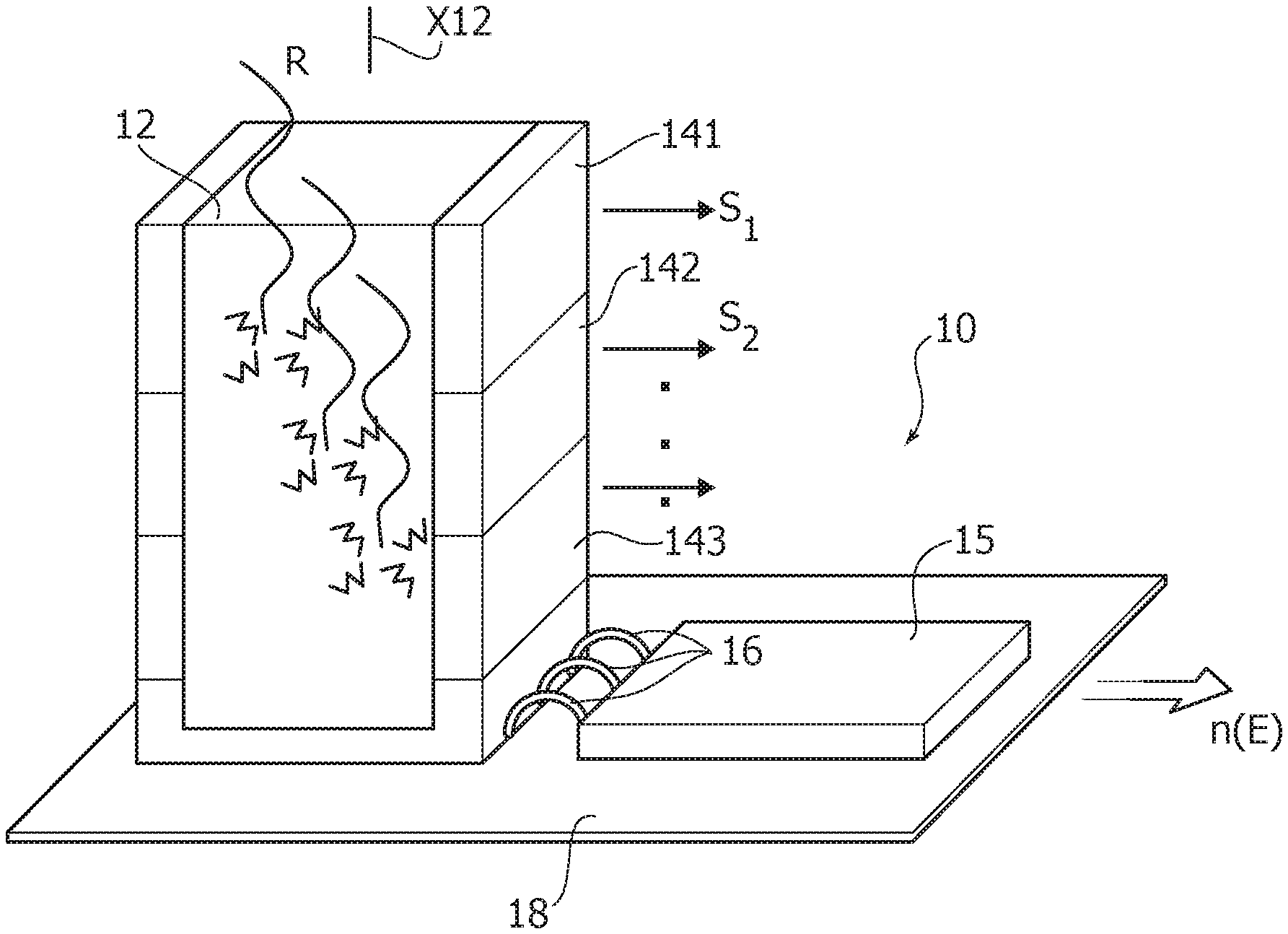
[0026] FIG. 1 is a perspective representation of a scintillator device.
[0027] The device 10 as shown in FIG. 1 may comprise a body of scintillator material such as a scintillator crystal 12 exposed to a radiation R.
[0028] The radiation R can be represented, for instance, by X rays or other types of ionizing radiations such as a particles, .beta. particles and .gamma. particles or other types emitted by radioactive material or radiation generators or generated by other following physical interaction.
[0029] The scintillator material 12 comprises material that exhibits scintillation, namely the property of luminescence when excited by (ionizing) radiation.
[0030] The scintillator material 12 may include CsI(Tl), thallium activated, cesium iodide. Other materials exhibiting scintillation are suitable for use in embodiments as discussed in the following.
[0031] Such a scintillator material may emit light, for instance infrared and/or visible photons, as a result of interaction with the radiation R.
[0032] The photons emitted as a result of scintillation can be received by a photodetector 14, that is a photoelectric converter configured to generate electrical signals of one or more output lines 16 as a result of converting the photons from the scintillator material into electrical signals.
[0033] The photoelectric converter 14 may include one or more Silicon PhotoMultipliers (SiPMs) or single-photon avalanche diodes (SPAD) operating in Geiger regime and capable of generating a current pulse when a photon hits a specific SPAD.
[0034] Reference to such types of photodetectors is for illustrative purposes only and is not to be construed as limiting the scope of the disclosure. Different types of photodetectors can be considered as alternative or additional embodiments.
[0035] For instance, the photoelectric converter 14 can comprise a bi-dimensional planar array of SPADs to provide an output signal which is the sum of the current pulses from the SPADs. A signal can thus be available on the electrical connections 16 between the detector 14 and the substrate 18, which is a function of, for instance, proportional to, the energy of the incident radiation R.
[0036] An array of SiPMs 14 can be considered with respective signals for the pixels in the array available in the connections 16, the planar distribution of the radiation R giving fluence and energy in the scintillator 12.
[0037] Such an output signal (electric signal) can be forwarded to associated processor circuitry 15, which can be wire bonded or flip chipped to the substrate 18 and be on a same circuit board 18 or hosted in a different package from the detector.
[0038] The processing circuitry 15 is configured to process such a signal, in various manners, for instance via software processing, with the possibility of presenting to a user information n(E) indicative of the energy spectrum of the radiation R detected.
[0039] The device 10 as shown in FIG. 1 can be incorporated to a portable electronic device such as a mobile phone or the like.
[0040] One or more embodiments may be based on the recognition that an arrangement as shown in FIG. 1 may be unable to take into account adequately the depth of interaction of the radiation R with the scintillator material 12.
[0041] Also, an arrangement as shown in FIG. 1 may be unable to provide a desirable detection efficiency for different radiation energies which may result in different thicknesses and material choices involved to adequately deposit its energy in the material.
[0042] One or more embodiments may address these issues by resorting to embodiments shown in FIGS. 2 to 5.
[0043] In FIGS. 2 to 5, parts or elements that are similar to the parts or elements already discussed in connection with FIG. 1 are indicated with like reference symbols. Therefore, a detailed description of these parts or elements will not be repeated in the case of FIGS. 2 to 5 for brevity.
[0044] As shown in FIGS. 2 to 4, one or more embodiments use a scintillator material body 12, for instance prismatic, such as parallelepiped, extending in at least one longitudinal direction X12 in combination with a plurality of photoelectric converters 141, 142, 143 distributed along the length of the scintillator material body 12 in the direction X12.
[0045] The signals S.sub.1, S.sub.2, . . . from these photoelectric converters 141, 142, 143 may be a function of a respective interaction position of the radiation R with the scintillator material 12, for instance, a respective depth of penetration of the radiation R into the scintillator material 12.
[0046] These different signals S.sub.1, S.sub.2, . . . resulting from photoelectric conversion of light produced by scintillation at different locations of the scintillator material body 12 may thus be forwarded towards the processing circuitry 15 with linearity correction processing applied therein to the signals S.sub.1, S.sub.2, . . . to provide a resulting detection signal n(E), which is a substantially linear function of the energy of the radiation R.
[0047] Such linearity correction processing may be of any type, which makes it unnecessary to provide a more detailed description herein. Also, it will be appreciated that one more embodiments may be primarily related to ways of producing the signals S.sub.1, S.sub.2, . . . rather than to processing thereof, which may be conducted by various means without limiting the scope of the disclosure.
[0048] FIGS. 3 and 4 are examples of the possibility of arranging at least one photoelectric converter or an array of photoelectric converters, 144, for instance, at a terminal position of the body of scintillator material 12. For instance, this may be at the "back" or "bottom" end of the body 12 opposed to the "front" or "top" end surface of the body 12 which is predominantly exposed to the radiation R.
[0049] For instance, in the case of a device 10 used as a dosimeter, the device may have a "front" or "top" sensing surface configured to be exposed to ionizing radiation R, with the scintillator body 12 having that end surface arranged facing the sensing surface so that light can be produced as a result of ionizing radiation R interacting with the scintillator material 12.
[0050] The overall mounting arrangement of FIGS. 3 and 4 may thus be similar to the one shown in FIG. 1, with the (other) photoelectric converters 141, 142, 143 distributed (staggered) along the lateral walls of the scintillator material body 12 along the longitudinal direction X12.
[0051] In one or more embodiments the "back" or "bottom" photoelectric converter 144 can be assembled on the substrate 18, via wires or bumps or other suitable connection means, with the scintillator body 12 placed on top of the photoelectric converters or detector 144 and the other "lateral" photoelectric converters 141, 142, 143 assembled vertically (with bumps for instance) along the longitudinal direction X12 of the body 12.
[0052] The arrangement of the detector shown herein is thus somewhat reminiscent of the vertical axis chip of an integrated 3-axis magnetometer System in Package (SiP) and similar processes can be used for its fabrication. Glue can be possibly considered for improving scintillator 12 and detector 144 coupling.
[0053] The processing circuitry 15 can then be assembled onto the substrate 18.
[0054] In one or more embodiments, for instance the lateral photoelectric converters 141, 142, . . . , can be assembled onto the scintillator material body 12 prior to placing the scintillator material body 12 onto the photoelectric converter 144.
[0055] FIG. 3 show example embodiments (for simplicity, this representation is provided in FIGS. 3 and 5 only) of embedding the scintillator material body 12 and the photoelectric converters 141, 142, . . . , in a material 2 capable of reflecting the photons, infrared and/or visible light photons, emitted by the scintillator material 12 as a result of interaction with the radiation R.
[0056] For instance, the material 2 can be a resin dispensed or molded such as a white-pigmented resin such as resin comprising titanium dioxide.
[0057] Such a resin can provide a reflectivity above 90%, possibly near 100%, in the region of the peak of emission of the scintillator material 12. It can also filter environmental light generated outside the device package and/or an additional material, a black resin for instance, may be molded "on top" to protect the overall structure and filter the external light.
[0058] For instance, in the case that the scintillator material 12 is a CsI(Tl) crystal, which has an emission peak at a wavelength of 550 nm and a lower wavelength cut-off at 320 nm, reflectivity of titanium dioxide of the material 2 may be above 90% from just above 400 nm in the case of the rutile form and even before in the case of atanase and remains well above 90% in the region of the peak, for instance reference can be made the Full Width at Half Maximum--FWHM.
[0059] It will be otherwise appreciated that, as discussed previously, reference to CsI(Tl) as a scintillator material is merely for illustration. Possible alternative choices may include, for instance, CsI(Na) or other alkali halide crystals or inorganic crystals. The choice of the material for the photon-reflective casing 2 may thus be adapted accordingly.
[0060] One or more embodiments may resort to arrangements where propagation paths of radiation coming down to different photoelectric converters may extend over different lengths and/or through different scintillator materials.
[0061] Such arrangements may involve, for instance, different materials juxtaposed to one another, for instance piled up in a stack and/or, as in the case shown in FIG. 5, arrangements where signals S.sub.1, S.sub.2, . . . , related to different propagation depths of the radiation X within a scintillator material can be produced by "splitting" the scintillator material 12 into a plurality of portions (bodies) of different lengths--and/or materials--as illustratively shown as 121, 122, 123, 124 in FIG. 5. The plurality of portions (bodies) 121, 122, 123, 124 each have a first surface 121U, 122U, 123U, 124U, respectively, that are distal from the substrate 18. The plurality of portions (bodies) 121, 122, 123, 124 each have a second surface (not shown in FIG. 5) that opposes the first surface 121U, 122U, 123U, 124U, respectively, and is proximal to the substrate 18. In some embodiments, the first surfaces 121U, 122U, 123U, 124U have different distances from the substrate 18. In some embodiments, the plurality of portions (bodies) 121, 122, 123, 124 have different dimensions in a direction between the first surface 121U, 122U, 123U, 124U and the respective second surface.
[0062] For instance, in one or more embodiments, scintillator material bodies 121, 122, 123, 124 can be provided having step-wise decreasing lengths corresponding to a desired detection efficiency for different radiation energies.
[0063] Moreover, the smallest lengths may contribute to the compensation of unlinearities in the processing of the signals S.sub.1, S.sub.2, . . . , in the "linearization" processing circuit 15, being a preliminary filter of the interaction depth of the lowest energy radiation particles.
[0064] While four scintillator material bodies 121, 122, 123, 124 are illustratively shown in FIG. 5, these bodies can be in any number, the number of four being just an example.
[0065] Also, in one or more embodiments, alternative or additional to scintillator material bodies 121, 122, 123, 124 having step-wise decreasing lengths as shown in FIG. 5, one or more scintillator material portions 121, 122, 123, 124 may have lengths and/or material that decrease or vary continuously, for instance with scintillator material portions 121, 122, 123, 124 similar to adjacent regions of a common scintillator material body or an adjacent separate scintillator material body. In one or more embodiments as shown in FIG. 5, the various scintillator material bodies 121, 122, 123, 124 can be juxtaposed by arranging them side-by-side by giving rise to a "columnar" arrangement.
[0066] Moreover, each scintillator body in the columnar arrangement in FIG. 5 may be equipped with lateral detectors as shown in FIG. 2 and FIG. 3.
[0067] The scintillator bodies may also be arranged in different 3D geometries, for instance one on top of the other instead of adjacent positions, or in spherical instead of planar geometry, depending on the radiation beam geometry.
[0068] In one or more embodiments as shown in FIG. 5, each of the bodies 121, 122, 123, 124 may have a respective photoelectric converter, for instance 142, 143, 144--a corresponding converter for the body 121 is not visible in FIG. 5, arranged at an end position, e.g., a back or bottom end, similar to the photoelectric converter 144 of FIG. 3, each one coupled to a respective electronic processing channel.
[0069] As shown in dashed lines, an arrangement as shown in FIG. 5 lends itself to the provision of a photon-reflecting casing 2 and/or a filtering case to prevent environmental photons to be detected as discussed previously in connection with FIG. 3.
[0070] In arrangements as shown in FIGS. 3 and 5, the photon-reflecting casing 2 applied or formed onto the scintillator material 12, 121, 122, 123, 124 and the associated phoetoelectric converters 141, 142, 143, 144 will counter undesired dispersion of photons so that the photons can be fully captured by the photoelectric converters.
[0071] A black resin (for instance a standard package molding compound for semiconductor devices: an epoxy molding compound or EMC may be exemplary of such a compound) may be eventually molded on the resulting structure, possibly including the processing circuitry, in manufacturing the relevant semiconductor devices.
[0072] One or more embodiments lend themselves to the simultaneous production of plural devices which can be eventually singulated to provide individual devices for instance in view of subsequent testing.
[0073] A device as shown herein (for instance, 10), may comprise: [0074] scintillator material (for instance, 12; 121, 122, 123, 124) configured to produce light as a result of radiation (for instance, R) interacting with the scintillator material, and [0075] photoelectric conversion circuitry (for instance, 141, 142, 143, 144) optically coupled to the scintillator material and configured to produce electrical signals (for instance, S.sub.1, S.sub.2, . . . ) via photoelectric conversion of light produced by the scintillator material, [0076] wherein the device comprises a plurality of photoelectric converters (for instance, 141, 142, 143, 144) optically coupled with said scintillator material at spatially separated (spatially distinct, for instance) locations, wherein the photoelectric converters in said plurality of photoelectric converters produce respective electrical signals by photoelectric conversion of light produced by the scintillator material as a result of radiation interacting with (propagating in, for instance) the scintillator material (along a plurality of respective propagation paths, for instance).
[0077] The scintillator material can be of different thicknesses (for instance, different lengths, as shown in FIG. 5) and/or comprise different materials, for instance, and the radiation may thus interact therewith (propagate therein, for instance) at respective propagation depths and/or in different materials.
[0078] For instance, in FIGS. 2 to 4, propagation paths of different lengths are provided extending from the "front" or "top" surface of the body 12 to the photoelectric converters 141, 142, 143, 144 spaced along the sides of the body 12 (and possibly at the bottom thereof: see, for instance, 144 in FIG. 3).
[0079] Still for instance, in FIG. 5 propagation paths of different lengths are provided between the "front" or "top" surfaces of the portions (bodies) 121, 122, 123, 124 and the "back" or "bottom" surfaces where the photoelectric converters 141, 142, 143, 144 are arranged.
[0080] A device as shown in FIGS. 2 to 4 may comprise at least one body of scintillator material extending, in a longitudinal direction (for instance, X12), wherein the photoelectric converters in said plurality of photoelectric converters may be coupled with said scintillator material at locations spatially separated along said longitudinal direction (X12).
[0081] In a device as shown herein, said plurality of photoelectric converters may comprise: [0082] at least one first photoelectric converter, for instance, 144, coupled with said body of scintillator material at an end or a terminal position thereof; [0083] at least one second photoelectric converter, for instance, 141, 142, 143, coupled with said body of scintillator material at a lateral position thereof.
[0084] A device as shown in FIG. 5 may comprise a plurality of portions of scintillator material (for instance, as separate bodies 121, 122, 123, 124) configured to produce light as a result of radiation interacting with the scintillator material (for different radiation energies), the portions in said plurality of portions of scintillator material having respective photoelectric converters optically coupled therewith.
[0085] In a device as shown in FIG. 5, the portions in said plurality of portions of scintillator material may have respective different thicknesses or lengths, for instance, and/or comprise different scintillator materials, thereby optimizing the detection efficiency for different radiation energies, the portions in said plurality of portions of scintillator material having respective photoelectric converters optically coupled therewith, at an end or a terminal position thereof for instance.
[0086] The portions in said plurality of portions of scintillator material may be juxtaposed to one another by being arranged side by side in a columnar arrangement, as shown in FIG. 5, and/or by being arranged in a piled or stacked arrangements or a combination of the two.
[0087] In a device as shown herein, said photoelectric converters may comprise silicon photomultipliers or arrays of SPADs of at least one pixel.
[0088] A device as shown herein may comprise a casing 2 of photon-reflective material surrounding said scintillator material and said plurality of photoelectric converters.
[0089] A device as shown herein may comprise a substrate 18 carrying said scintillator material and said plurality of photoelectric converters as well as signal processing circuitry 15 coupled to said plurality of photoelectric converters and configured to process the electrical signals produced by said plurality of photoelectric converters.
[0090] A dosimeter as shown herein may have a sensing surface configured to be exposed to ionizing radiation, the dosimeter comprising a device as shown herein, the device arranged with said scintillator material facing said sensing surface to produce light as a result of ionizing radiation interacting with the scintillator material.
[0091] Without prejudice to the underlying principles, the details and embodiments may vary, even significantly, with respect to what has been described by way of example only without departing from the scope of protection.
[0092] The various embodiments described above can be combined to provide further embodiments.
[0093] These and other changes can be made to the embodiments in light of the above-detailed description. In general, in the following claims, the terms used should not be construed to limit the claims to the specific embodiments disclosed in the specification and the claims, but should be construed to include all possible embodiments along with the full scope of equivalents to which such claims are entitled. Accordingly, the claims are not limited by the disclosure.
* * * * *
D00000
D00001
D00002
D00003
XML
uspto.report is an independent third-party trademark research tool that is not affiliated, endorsed, or sponsored by the United States Patent and Trademark Office (USPTO) or any other governmental organization. The information provided by uspto.report is based on publicly available data at the time of writing and is intended for informational purposes only.
While we strive to provide accurate and up-to-date information, we do not guarantee the accuracy, completeness, reliability, or suitability of the information displayed on this site. The use of this site is at your own risk. Any reliance you place on such information is therefore strictly at your own risk.
All official trademark data, including owner information, should be verified by visiting the official USPTO website at www.uspto.gov. This site is not intended to replace professional legal advice and should not be used as a substitute for consulting with a legal professional who is knowledgeable about trademark law.