Clock And Data Recovery Devices With Fractional-n Pll
TALEGAONKAR; Mrunmay ; et al.
U.S. patent application number 17/013307 was filed with the patent office on 2020-12-24 for clock and data recovery devices with fractional-n pll. The applicant listed for this patent is INPHI CORPORATION. Invention is credited to Aaron BUCHWALD, Karthik Gopalakrishnan, Belal HELAL, Yu LIAO, Chang-Feng LOI, Jorge PERNILLO, Praveen PRABHA, Jamal RIANI, Junyi SUN, Mrunmay TALEGAONKAR.
| Application Number | 20200403627 17/013307 |
| Document ID | / |
| Family ID | 1000005076747 |
| Filed Date | 2020-12-24 |


View All Diagrams
| United States Patent Application | 20200403627 |
| Kind Code | A1 |
| TALEGAONKAR; Mrunmay ; et al. | December 24, 2020 |
CLOCK AND DATA RECOVERY DEVICES WITH FRACTIONAL-N PLL
Abstract
The present invention relates to data communication and electrical circuits. More specifically, embodiments of the present invention provide a clock and data recovery (CDR) architecture implementation for high data rate wireline communication links. In an embodiment, a CDR device includes a phase detector, a loop filter, and a fractional-N PLL. The fractional-N PLL generates output clock signal based on output of the loop filter. There are other embodiments as well.
| Inventors: | TALEGAONKAR; Mrunmay; (Laguna Hills, CA) ; PERNILLO; Jorge; (Daly City, CA) ; SUN; Junyi; (Singapore, SG) ; PRABHA; Praveen; (Lake Forest, CA) ; LOI; Chang-Feng; (Singapore, SG) ; LIAO; Yu; (Longmont, CO) ; RIANI; Jamal; (Fremont, CA) ; HELAL; Belal; (Santa Clara, CA) ; Gopalakrishnan; Karthik; (Cupertino, CA) ; BUCHWALD; Aaron; (Newport Beach, CA) | ||||||||||
| Applicant: |
|
||||||||||
|---|---|---|---|---|---|---|---|---|---|---|---|
| Family ID: | 1000005076747 | ||||||||||
| Appl. No.: | 17/013307 | ||||||||||
| Filed: | September 4, 2020 |
Related U.S. Patent Documents
| Application Number | Filing Date | Patent Number | ||
|---|---|---|---|---|
| 16127103 | Sep 10, 2018 | 10804913 | ||
| 17013307 | ||||
| Current U.S. Class: | 1/1 |
| Current CPC Class: | H03L 7/0807 20130101; H03L 7/087 20130101; H03L 7/099 20130101; H03L 7/1976 20130101; H04L 7/0331 20130101 |
| International Class: | H03L 7/197 20060101 H03L007/197; H04L 7/033 20060101 H04L007/033; H03L 7/087 20060101 H03L007/087; H03L 7/08 20060101 H03L007/08; H03L 7/099 20060101 H03L007/099 |
Claims
1. A clock data recovery (CDR) device comprising: a first phase detection module configured to receive digital input signal and determine a difference between the digital input signal and an output clock signal, the first phase detection module being configured to determine a scaling factor in situ based on a gain mismatch; a loop filter module coupled to the first phase detection module and configured to generate a frequency control word; and a fractional-N phase lock loop (Frac-N PLL) configured to generate the output clock signal based on the frequency control word; wherein the Frac-N PLL comprises: a second phase detection module coupled to a reference clock signal; a charge pump coupled to the second phase detection module; an analog loop filter coupled to the charge pump; a sigma delta modulator configured to process the frequency control word.
2. The CDR device of claim 1 wherein the gain mismatch is calculated using a feedback signal path.
3. The CDR device of claim 2 wherein the feedback signal path comprises a digital square signal input and a triangular signal output.
4. The CDR device of claim 3 wherein where the first phase detection module is configured to determine a peak-to-peak value of the triangular signal output, the triangular signal output being obtained at a phase detector output.
5. The CDR device of claim 1 wherein the Frac-N PLL further comprises a multi-modulus divider coupled to the signal delta modulator.
6. The CDR device of claim 1 wherein the Frac-N PLL further comprises a digital high-pass filter.
7. The CDR device of claim 6 wherein the digital high-pass filter comprises an inverse filter and an anti-aliasing filter.
8. The CDR device of claim 1 wherein the Frac-N PLL further comprises a feedforward loop.
9. The CDR device of claim 8 wherein the charge pump is configured on the feedforward loop.
10. The CDR device of claim 8 wherein the Frac-N PLL further comprises a voltage-controlled oscillator configured on the feedforward loop.
11. A clock data recovery (CDR) device comprising: a first phase detection module configured to receive digital input signal and determine a difference between the digital input signal and an output clock signal, the first phase detection module being configured to output triangular signals based on square signals, a gain scaling factor being determined using the triangular signals and the square signals; a loop filter module coupled to the first phase detection module and configured to generate a frequency control word; and a fractional-N phase lock loop (Frac-N PLL) configured to generate the output clock signal based on the frequency control word, the Frac-N PLL comprising a high-pass filter for processing the frequency control word, the high-pass filter comprising an inverse filter and an anti-aliasing filter.
12. The CDR device of claim 11 wherein the CDR devices is configured to use the gain scaling factor to correct a gain mismatch.
13. The CDR device of claim 12 wherein the gain mismatch is determined using at least a peak-to-peak value of the triangular signals.
14. The CDR device of claim 11 wherein the Frac-N PLL further comprises a charge pump.
15. The CDR device of claim 11 wherein the anti-aliasing filter is implemented as a digital FIR filter.
16. A clock data recovery (CDR) device comprising: a first phase detection module configured to receive digital input signal and determine a difference between the digital input signal and an output clock signal; a loop filter module coupled to the first phase detection module and configured to generate a frequency control word; and a fractional-N phase lock loop (Frac-N PLL) configured to generate the output clock signal based on the frequency control word, the Frac-N PLL comprising a voltage controlled oscillator configured on a feedforward signal path and a current mode digital-to-analog converter; wherein the feedforward signal path comprises a square input signal and an output triangular signal, a digital gain scaling factor being determined using the square input signal and the output triangular signal.
17. The CDR device of claim 16 wherein the digital gain scaling factor is used to correct a gain mismatch, the gain mismatch being based on a peak-to-peak value of the output triangular signal.
18. The CDR device of claim 16 wherein the first phase detection module is configured to calibrate a gain parameter of the Frac-N PLL based at least on the output clock signal.
19. The CDR device of claim 18 wherein the first phase detection module is coupled to a reference clock signal.
20. The CDR device of claim 16 wherein the Frac-N PLL further comprises a multi-modulus divider.
Description
CROSS-REFERENCES TO RELATED APPLICATIONS
[0001] The present invention is a continuation application to U.S. patent application Ser. No. 16/127,103, filed on 10 Sep. 2018, entitled "CLOCK AND DATA RECOVERY DEVICES WITH FRACTIONAL-N PLL", which is incorporated by reference herein for all purposes.
STATEMENT AS TO RIGHTS TO INVENTIONS MADE UNDER FEDERALLY SPONSORED RESEARCH AND DEVELOPMENT
[0002] NOT APPLICABLE
REFERENCE TO A "SEQUENCE LISTING," A TABLE, OR A COMPUTER PROGRAM LISTING APPENDIX SUBMITTED ON A COMPACT DISK
[0003] NOT APPLICABLE
BACKGROUND OF THE INVENTION
[0004] The present invention relates to data communication and electrical circuits.
[0005] Over the last few decades, the use of communication networks has exploded. In the early days of the Internet, popular applications were limited to emails, bulletin board, and mostly informational and text-based web page surfing, and the amount of data transferred was usually relatively small. Today, Internet and mobile applications demand a huge amount of bandwidth for transferring photo, video, music, and other multimedia files. For example, a social network like Facebook processes more than 500 TB of data daily.
[0006] Clock and data recovery (CDR) devices are used in a wide range of applications. For example, to process data received over a communication network, a receiver relies on its CDR to generate a clock signal based on the received data. The performance of the receiver relies on the performance of its CDR and other components. Over the time, there have been many different types of CDR designs and implementations, however, they have been inadequate for the reasons explained below. Therefore, new and improved CDR devices are desired.
BRIEF SUMMARY OF THE INVENTION
[0007] The present invention relates to data communication and electrical circuits. More specifically, embodiments of the present invention provide a clock and data recovery (CDR) architecture implementation for high data rate wireline communication links. In an embodiment, a CDR device includes a phase detector, a loop filter, and a fractional-N PLL. The fractional-N PLL generates output clock signal based on output of the loop filter. There are other embodiments as well.
[0008] According to an embodiment, the present invention provides A clock data recovery (CDR) device, which includes a first phase detection module configured to receive digital input signal and determine a difference between phases of the digital input signal and an output clock signal. The device additionally includes a loop filter module coupled to the phase detector module and configured to generate a frequency control word. The device also includes a fractional-N phase lock loop (Frac-N PLL) configured to generate the output clock signal based on the frequency control word. The Frac-N PLL includes a second phase detection module coupled to a reference clock signal. The Frac-N PLL also includes a charge pump coupled to the second phase detection module. The Frac-N PLL additionally includes an analog loop filter coupled to the charge pump. The Frac-N PLL also includes a sigma delta modulator configured to process the frequency control word.
[0009] According to another embodiment, the present invention provides a clock data recovery (CDR) device that includes a first phase detection module configured to receive digital input signal and determine a difference between phases of the digital input signal and an output clock signal. The device also includes a loop filter module coupled to the phase detector module and configured to generate a frequency control word. The device additionally includes a fractional-N phase lock loop (Frac-N PLL) configured to generate the output clock signal based on the frequency control word, the Frac-N PLL comprising a high-pass filter for processing the frequency control word. The high-pass filter has an inverse filter and an anti-aliasing filter.
[0010] According to yet another embodiment, the present invention provides a clock data recovery (CDR) device, which has a first phase detection module configured to receive digital input signal and determine a difference between the digital input signal and an output clock signal. The device also includes a loop filter module coupled to the phase detector module and configured to generate a frequency control word. The device additionally includes a fractional-N phase lock loop (Frac-N PLL) configured to generate the output clock signal based on the frequency control word. The Frac-N PLL has a voltage controlled oscillator configured on a feedforward signal path and a current mode digital-to-analog converter.
[0011] It is to be appreciated that embodiments of the present invention provide many advantages over conventional techniques. Among other things, CDR devices implemented according to embodiments of the present invention are smaller and more efficient compared to existing devices (e.g., phase-interpolator or digitally controlled oscillator implementations). For example, compared to CDRs with digitally controlled oscillators, CDRs with fractional-N PLL have better immunity to various types of coupling noise. Additionally, a fractional-N PLL based CDR can provide independent gain suitable for the CDR device.
[0012] Embodiments of the present invention can be implemented in conjunction with existing systems and processes. For example, CDR devices implemented with Frac-N PLLs according to the present invention can be used for a wide range of applications and are compatible with existing systems and architectures. Additionally, CDR devices according to the present invention can be manufactured using existing manufacturing processes and equipment. There are other benefits as well.
[0013] The present invention achieves these benefits and others in the context of known technology. However, a further understanding of the nature and advantages of the present invention may be realized by reference to the latter portions of the specification and attached drawings.
BRIEF DESCRIPTION OF THE DRAWINGS
[0014] The following diagrams are merely examples, which should not unduly limit the scope of the claims herein. One of ordinary skill in the art would recognize many other variations, modifications, and alternatives. It is also understood that the examples and embodiments described herein are for illustrative purposes only and that various modifications or changes in light thereof will be suggested to persons skilled in the art and are to be included within the spirit and purview of this process and scope of the appended claims.
[0015] FIG. 1 is a simplified diagram illustrating a fractional-N PLL according to an embodiment of the present invention.
[0016] FIG. 2 provides a small signal model of a multi-modulus divider according to embodiments of the present invention.
[0017] FIG. 3 is a simplified diagram illustrating a digitally controlled oscillator (DCO) based CDR loop.
[0018] FIG. 4 is a simplified diagram illustrating a Frac-N PLL incorporated inside a CDR loop according to embodiments of the present invention.
[0019] FIG. 5 is a simplified diagram illustrating small signal phase domain model of a CDR loop with a DCO.
[0020] FIG. 6 is a simplified diagram illustrating a small signal model of Frac-N PLL functioning as a DCO according to embodiments of the present invention.
[0021] FIG. 7 is a plot illustrating CDR error transfer functions comparing ideal DCO and actual DCO implementation (e.g., with Frac-N PLL) with a pole that contributes to undesired error transfer function peaking.
[0022] FIG. 8 provides plots illustrating CDR error transfer function peaking (top) and Frac-N PLL jitter (bottom) as function of Frac-N PLL bandwidth.
[0023] FIG. 9 is a simplified diagram illustrating a small signal model for a Frac-N PLL according to embodiments of the present invention.
[0024] FIG. 10 is a simplified diagram illustrating a digital high-pass filter according to embodiments of the present invention.
[0025] FIG. 11 provides plots showing simulated CDR error transfer function peaking (top) and output jitter (bottom) as function of Frac-N PLL bandwidth with digital high-pass filter.
[0026] FIG. 12 is a simplified diagram illustrating a small signal model for a Frac-N PLL with charge pump according to embodiments of the present invention.
[0027] FIG. 13 is a simplified diagram illustrating a Frac-N PLL implementation with a charge pump according to embodiments of the present invention.
[0028] FIG. 14 shows the simulated CDR error transfer function peaking (top) and output jitter (bottom) as function of Frac-N PLL bandwidth with charge pump in the feedforward path.
[0029] FIG. 15 is a simplified small signal model for a Frac-N PLL with feed-forward VCO path according to embodiments of the present invention.
[0030] FIG. 16 is a simplified diagram illustrating a Frac-N PLL implemented with feed-forward VCO path according to embodiments of the present invention.
[0031] FIG. 17 shows the simulated CDR error transfer function peaking (top) and output jitter (bottom) as function of Frac-N PLL bandwidth with a feed-forward VCO path.
[0032] FIG. 18 shows the effect of gain mismatch on CDR error transfer function peaking.
[0033] FIG. 19 is a simplified block diagram illustrating feedforward gain calibration for Frac-N PLL implementation of CDR according to embodiments of the present invention.
[0034] FIG. 20 shows transfer functions for each of the two paths. It is to be noted that signal injected in Frac-N PLL path at frequency F.sub.2 has the same gain compared to the signal injected at frequency F.sub.1 in the feedforward path.
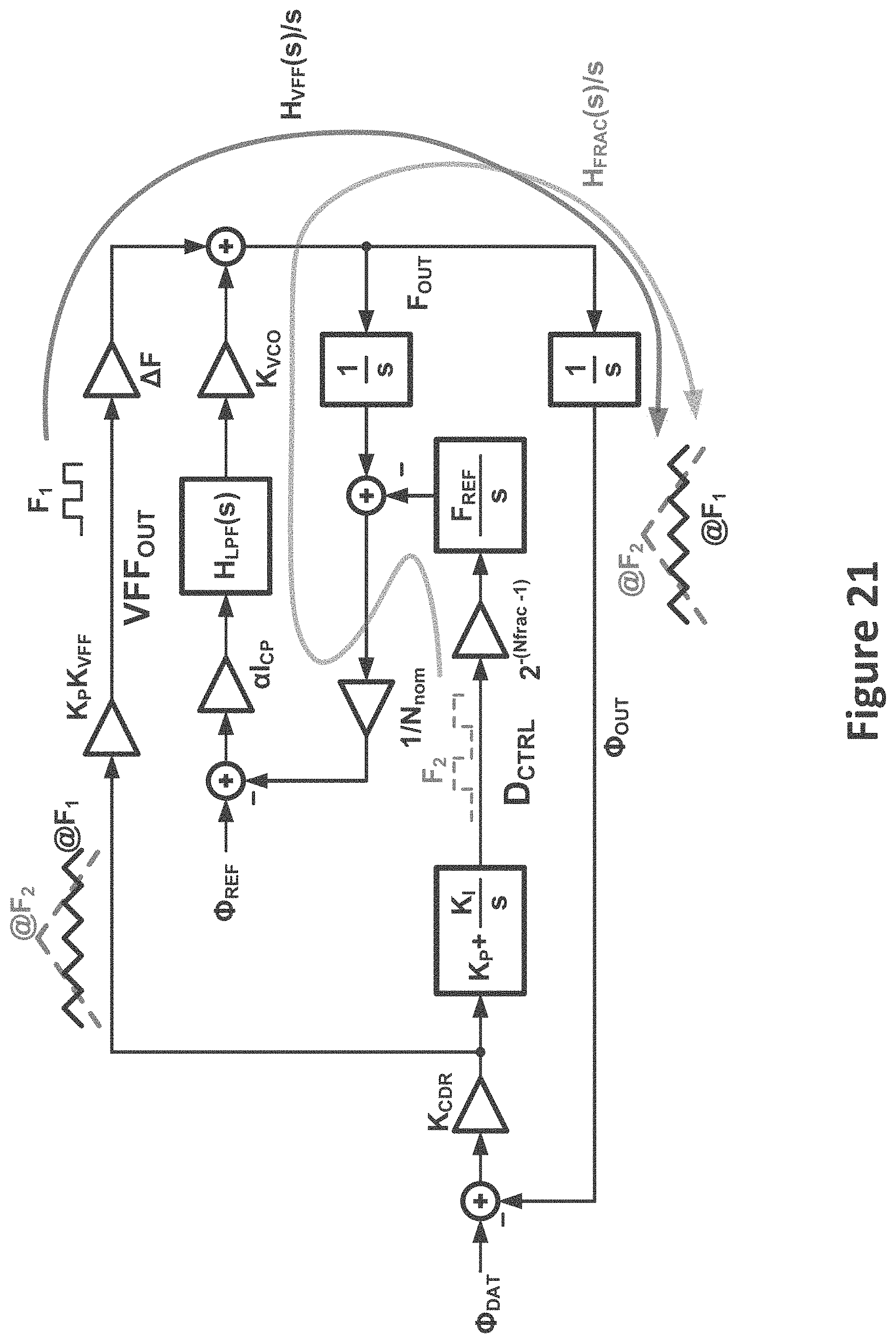
[0035] FIG. 21 is a simplified diagram illustrating a feedforward configuration with injected signals according to embodiments of the present invention.
[0036] FIG. 22 provides simulation results of a feedforward implementation according to embodiments of the present invention.
DETAILED DESCRIPTION OF THE INVENTION
[0037] The present invention relates to data communication and electrical circuits. More specifically, embodiments of the present invention provide a clock and data recovery (CDR) architecture implementation for high data rate wireline communication links. In an embodiment, a CDR device includes a phase detector, a loop filter, and a fractional-N PLL. The fractional-N PLL generates output clock signal based on output of the loop filter. There are other embodiments as well.
[0038] Low-jitter CDR architectures are often an essential aspect for high data rate wireline receivers. While some of the early CDRs utilized analog voltage-controlled oscillator (VCO) based architectures, phase interpolator (PI)-based clock data recovery (CDR) modules have come to dominate CDR loop implementations due to their relative small-area (as compared to other designs and architectures) and digital control functionality. A shift towards analog-to-digital converter (ADC) based receivers (thus moving from analog to digital) has made digital control necessary for CDR loop implementations. Phase interpolators provide this functionality by converting digital phase control input signal to analog clock phase shift signal at the output. Performance of a PI in a CDR implementation requires high linearity, high output phase resolution, and high-clock-frequency operation. Unfortunately, designing highly linear PIs with high output phase resolution at high clock frequency is difficult.
[0039] As a result, CDR architectures utilizing PIs struggle to achieve the low-jitter performance criteria needed for high data rate operation. An alternative to PI-based CDR is a digitally controlled oscillator (DCO) based CDR architecture. The low-jitter requirement mentioned above precludes the use of ring oscillator based DCOs applications that require high data rates. For example, LC-based DCO (LC DCO) can potentially provide low jitter, but they are susceptible to electromagnetic coupling due to low CDR bandwidth achieved by typical high data rate links.
[0040] It is thus to be appreciated that embodiments of the present invention provide high-performance CDRs implemented with fractional-N (Frac-N) phase-lock loops (PLL). More specifically, embodiments of the present invention provide CDRs with wide bandwidth Frac-N PLLs to provide the functionalities of digitally controlled oscillators and reduce susceptibility of LC-VCOs to electromagnetic coupling, while providing low jitter digital phase shift capability to CDR loops. In an exemplary embodiment, a CDR architecture is designed to eliminate the need for phase interpolator (PI) by employing fractional-N phase-locked loop (PLL), and it is capable of achieving low-jitter performance critical for high-data rate applications. The present invention also provides methods to ensure CDR loop stability. The present invention additionally provides calibration technique to ensure robust operation. As an example, the following techniques are provided: [0041] Use of fractional-N (analog or digital) PLLs in CDR loops for phase and frequency tracking; [0042] Digital high-pass filter based technique for compensating adverse effects (such as stability and error transfer function peaking) caused due to introduction of Frac-N PLL in CDR loop; [0043] Charge pump feedforward techniques for compensating adverse effects (such as stability and error transfer function peaking) caused due to introduction of Frac-N PLL in CDR loop; [0044] A variation of this technique can be used for digital fractional-N PLLs; [0045] VCO feedforward techniques for compensating adverse effects (such as stability and error transfer function peaking) caused due to introduction of an analog or digital Frac-N PLL in CDR loop; [0046] VCO feedforward gain calibration techniques for in-situ calibration of parallel path gain mismatch in VCO feedforward scheme.
[0047] The following description is presented to enable one of ordinary skill in the art to make and use the invention and to incorporate it in the context of particular applications. Various modifications, as well as a variety of uses in different applications will be readily apparent to those skilled in the art, and the general principles defined herein may be applied to a wide range of embodiments. Thus, the present invention is not intended to be limited to the embodiments presented, but is to be accorded the widest scope consistent with the principles and novel features disclosed herein.
[0048] In the following detailed description, numerous specific details are set forth in order to provide a more thorough understanding of the present invention. However, it will be apparent to one skilled in the art that the present invention may be practiced without necessarily being limited to these specific details. In other instances, well-known structures and devices are shown in block diagram form, rather than in detail, in order to avoid obscuring the present invention.
[0049] The reader's attention is directed to all papers and documents which are filed concurrently with this specification and which are open to public inspection with this specification, and the contents of all such papers and documents are incorporated herein by reference. All the features disclosed in this specification, (including any accompanying claims, abstract, and drawings) may be replaced by alternative features serving the same, equivalent or similar purpose, unless expressly stated otherwise. Thus, unless expressly stated otherwise, each feature disclosed is one example only of a generic series of equivalent or similar features.
[0050] Furthermore, any element in a claim that does not explicitly state "means for" performing a specified function, or "step for" performing a specific function, is not to be interpreted as a "means" or "step" clause as specified in 35 U.S.C. Section 112, Paragraph 6. In particular, the use of "step of" or "act of" in the Claims herein is not intended to invoke the provisions of 35 U.S.C. 112, Paragraph 6.
[0051] Please note, if used, the labels left, right, front, back, top, bottom, forward, reverse, clockwise and counter clockwise have been used for convenience purposes only and are not intended to imply any particular fixed direction. Instead, they are used to reflect relative locations and/or directions between various portions of an object.
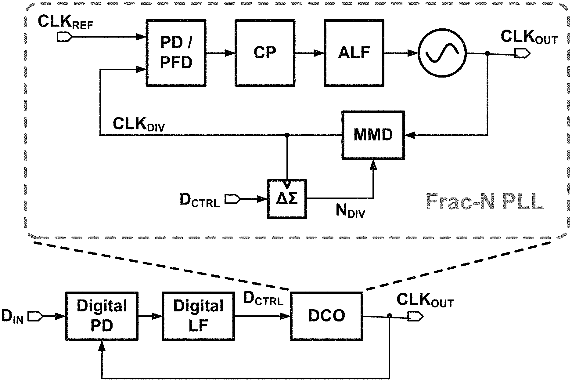
[0052] FIG. 1 is a simplified diagram illustrating a fractional-N PLL according to an embodiment of the present invention. This diagram is merely an example, which should not unduly limit the scope of the claims. One of ordinary skill in the art would recognize many variations, alternatives, and modifications. The PLL includes a phase detector (PD) or phase and frequency detector (PFD), a charge pump (CP), an analog loop filter (ALF), a voltage-controlled oscillator (VCO), multi-modulus divider (MMD), and a digital .DELTA..SIGMA. modulator (.DELTA..SIGMA.). The input reference clock is denoted as CLK.sub.REF, and the output clock is denoted as CLK.sub.OUT. A high resolution digital frequency control signal, D.sub.CTRL, is converted to an integer division ratio, N.sub.DIV, by a digital .DELTA..SIGMA. modulator. The output of the multi-modulus divider (MMD) is divided clock signal denoted as CLK.sub.DIV. The output frequency, F.sub.OUT, of such a fractional-N PLL depends on the input reference frequency F.sub.REF and D.sub.CTRL, which is described in Equation 1 below:
F.sub.OUT=D.sub.CTRLF.sub.REF Equation 1:
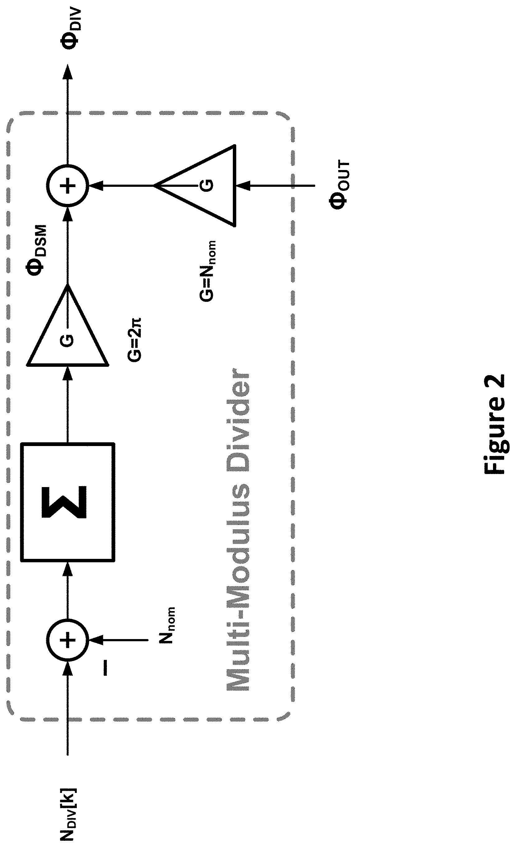
[0053] It is to be noted that D.sub.CTRL can be used to control not only the output frequency, but also the output phase of the Frac-N PLL. FIG. 2 provides a small signal model of a multi-modulus divider according to embodiments of the present invention. This diagram is merely an example, which should not unduly limit the scope of the claims. One of ordinary skill in the art would recognize many variations, alternatives, and modifications. It can be shown that the overall output phase of the MMD is given by Equation 2 below:
.PHI. DIV ( z ) = N n o m .PHI. O U T ( z ) + 2 .pi. ( N DIV ( z ) - N n o m ) ( z - 1 1 - z - 1 ) Equation 2 ##EQU00001##
[0054] where .PHI..sub.DIV is the phase of the divider output, .PHI..sub.OUT is the phase of the fractional-N PLL output that is input to the MMD, N.sub.nom denotes the nominal division ratio of the fractional-N PLL, and N.sub.DIV denotes the instantaneous integer division ratio of MMD.
[0055] Equation 2 can be expressed as Equation 3:
.PHI. DIV ( z ) = N n o m .PHI. O U T ( z ) + 2 .pi. ( D C T R L ( z ) S T F ( z ) - N n o m ) ( z - 1 1 - z - 1 ) Equation 3 ##EQU00002##
[0056] where STF(z) is the signal transfer function of the digital .DELTA..SIGMA. modulator and D.sub.CTRL denotes the digital frequency control input. If we assume an ideal reference clock for the Frac-N PLL (i.e., .PHI..sub.DIV=0), the output phase is given by Equation 4 below:
.PHI. O U T ( z ) = - 2 .pi. N n o m ( D C T R L ( z ) S T F ( z ) - N n o m ) ( z - 1 1 - z - 1 ) Equation 4 ##EQU00003##
[0057] Equation 4 shows that the output phase of the Frac-N PLL can be controlled using digital frequency control signal, D.sub.CTRL.
[0058] FIG. 3 is a simplified diagram illustrating a DCO-based CDR loop. The phase difference between incoming data, DIN, and sampling clock CLK.sub.OUT is detected by a digital phase detector (Digital PD). As an example, a proportional-integral path based digital loop filter (Digital LF) is used to generate a digital frequency control word D.sub.CTRL for the DCO. The output frequency F.sub.OUT of the DCO depends on D.sub.CTRL, and the output frequency (F.sub.OUT) of the DCO (characterized by a DCO gain, K.sub.DCO) is described in Equation 5 below:
F.sub.OUT=D.sub.CTRLK.sub.DCO Equation 5:
[0059] It is to be appreciated that there are similarities between DCO and Frac-N PLL. In particular, the functionality of Frac-N PLL in CDR implementations according to embodiments of the present invention is equivalent to a digitally controlled oscillator (DCO), with the functional characteristics K.sub.DCO=F.sub.REF. In various embodiments, a Frac-N PLL is used as a functional equivalent of a DCO in a CDR loop. Compared to a stand-alone LC DCO implementation, a wide bandwidth Frac-N PLL provides better immunity to VCO coupling noise. Due to its closed loop operation, it also provides a DCO implementation with a well-defined process independent DCO gain, K.sub.DCO.
[0060] FIG. 4 is a simplified diagram illustrating a Frac-N PLL incorporated inside a CDR loop according to embodiments of the present invention. This diagram is merely an example, which should not unduly limit the scope of the claims. One of ordinary skill in the art would recognize many variations, alternatives, and modifications. The digital frequency control word D.sub.CTRL (generated for CDR loop) is used as a frequency control input for a Frac-N PLL. The output clock generated by Frac-N PLL, CLK.sub.OUT, is used as a sampling clock for the CDR loop.
[0061] As explained above, Frac-N PLL in FIG. 4 provides functionalities and advantages of an LC DCO without its penalties as used in a CDR. As an example, Frac-N PLL includes a phase detector (PD) or a phase-frequency detector (PFD) for phase detection, a charge pump for compensation, an analog loop filter (ALF) for filtering. The Frac-N PLL additionally includes an oscillator, an MMD, and a digital .DELTA..SIGMA. modulator. It is to be appreciated that Frac-N PLL can be implemented in other ways as well. It is to be understood CDRs according to the present invention can be implemented using analog Frac-N PLLs or digital Frac-N PLLs.
[0062] The incorporation of a Frac-N PLL in a CDR also contributes to certain functional difference from an LC DCO implementation. After all, a Frac-N PLL is not the same as an LC DCO. More specifically, while a Frac-N PLL has well-defined gain at low frequencies, its gain rolls off at high frequencies due to low pass nature of the PLL. FIG. 5 is a simplified diagram illustrating small signal phase domain model of a CDR loop with a DCO.
[0063] In case of an ideal DCO, the gain is independent of frequency, (i.e., K.sub.DCO(S)=K.sub.DCO, where s is the reference modulation frequency). The digital loop filter is chosen to achieve appropriate CDR closed loop bandwidth and jitter tolerance. On the other hand, when Frac-N PLL is used (instead of DCO), the gain is given by K.sub.DCO(S)=F.sub.REFG(s), where G(s) is effective low-pass transfer function of the Frac-N PLL. Due to its low-pass nature, G(s) introduces additional poles in the CDR loop transfer function, which adversely affects the CDR loop stability and creates peaking in the CDR error transfer function E(s), where E(s) is defined by E(s)=.PHI..sub.E(s)/.PHI..sub.IN(s), subsequently degrading the jitter tolerance of the CDR loop. Note that jitter tolerance and error transfer function are related as JTOL(s)=1/E(s).
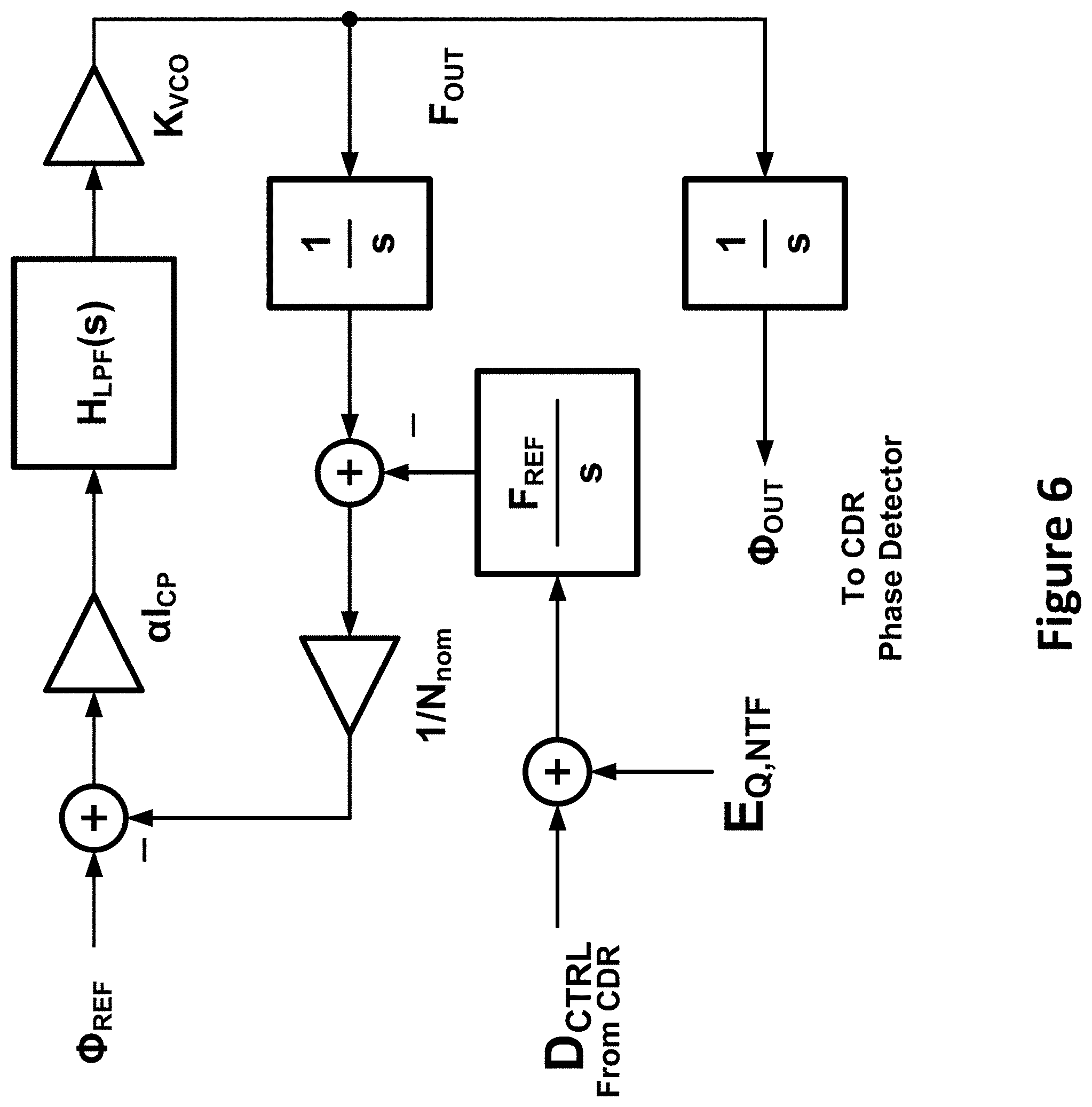
[0064] FIG. 6 is a simplified diagram illustrating a small signal model of Frac-N PLL functioning as a DCO according to embodiments of the present invention. This diagram is merely an example, which should not unduly limit the scope of the claims. One of ordinary skill in the art would recognize many variations, alternatives, and modifications. The function F.sub.OUT(s) represents the output frequency of the Frac-N PLL, while .PHI..sub.OUT(s) represents its phase. The high-pass shaped quantization noise of the digital .DELTA..SIGMA. modulator is denoted as E.sub.Q,NTF(s). The behavior of the Frac-N PLL is described in Equation 6 below:
F O U T ( s ) D C T R L ( s ) = F OUT ( s ) E Q , NTF ( s ) = F R E F G ( s ) Where , G ( s ) = L G ( s ) 1 + L G ( s ) Equation 6 ##EQU00004##
[0065] In Equation 6, LG(s) denotes the open loop gain of the Frac-N PLL. To reduce CDR error transfer function E(s) peaking, the implementation needs to increase the bandwidth of Frac-N PLL and by extending the bandwidth of G(s). This increased bandwidth, however, allows more noise from digital .DELTA..SIGMA. pass through. As a result, there is a trade-off between peaking of E(s) and the output jitter of the Frac-N PLL. FIG. 7 is a plot illustrating CDR error transfer functions comparing ideal DCO and actual DCO implementation (e.g., with Frac-N PLL) with a pole that contributes to undesired error transfer function peaking.
[0066] FIG. 8 provides plots illustrating CDR error transfer function peaking (top) and Frac-N PLL jitter (bottom) as function of Frac-N PLL bandwidth. As can be seen in FIG. 8, the peaking is reduced at higher PLL bandwidth at the cost of worse jitter performance. For optimal system performance, the implementation needs to reduce the bandwidth for F.sub.OUT(S)/E.sub.Q,NTF(s) while maximizing the bandwidth for F.sub.OUT(s)/D.sub.CTRL(s).
[0067] In various embodiments, the present invention provides feedforward techniques to compensate the bandwidth limitations of Frac-N PLL. The problem discussed in the previous section can be solved by introducing a feedforward path from D.sub.CTRL(s) to F.sub.OUT(s). Such a feedforward path can decouple the transfer function seen by D.sub.CTRL(s) from the transfer function seen by E.sub.Q,NTF(s). We propose the following methods for implementing the feedforward path.
[0068] According to a specific embodiment, a Frac-N PLL is implemented in a CDR with a digital high-pass filter. FIG. 9 is a simplified diagram illustrating a small signal model for a Frac-N PLL according to embodiments of the present invention. This diagram is merely an example, which should not unduly limit the scope of the claims. One of ordinary skill in the art would recognize many variations, alternatives, and modifications. It is to be appreciated that the addition of a digital high-pass filter in the D.sub.CTRL path can effectively counter the low-pass nature of G(s). In this case, the DCO (i.e., DCO equivalent implemented with Frac-N PLL as used in a CDR) transfer function is given by Equation 7 below:
F O U T ( s ) D C T R L ( s ) = F R E F H 1 ( s ) G ( s ) Equation 7 ##EQU00005##
[0069] It is to be noted that the transfer function from E.sub.Q,NTF to F.sub.OUT remains unchanged. For example, for H.sub.1(s)=G.sup.-1(s), Equation 8 below is obtained:
F OUT ( s ) D C T R L ( s ) = F R E F G - 1 ( s ) G ( s ) = F R E F Equation 8 ##EQU00006##
[0070] In practical implementations, a digital finite impulse response (FIR) filter can be used to approximately match the inverse of G(s). Furthermore, there is a possibility of noise in D.sub.CTRL signal folding back in Frac-N PLL in-band frequency region due to up-sampling in the Frac-N PLL. To alleviate this undesirable effect of out of band noise, an anti-aliasing filter is also provided in the D.sub.CTRL path. This anti-aliasing filter can also be implemented as a digital FIR filter. FIG. 10 is a simplified diagram illustrating a digital high-pass filter according to embodiments of the present invention. This diagram is merely an example, which should not unduly limit the scope of the claims. One of ordinary skill in the art would recognize many variations, alternatives, and modifications. For example, a digital high pass filter H.sub.1(s) includes an inverse filter H.sub.1(z) and an anti-aliasing filter AA(z).
[0071] FIG. 11 provides plots showing simulated CDR error transfer function peaking (top) and output jitter (bottom) as function of Frac-N PLL bandwidth with digital high-pass filter. It can be seen that the CDR error transfer function peaking becomes almost independent of Frac-N PLL bandwidth. This allows for a Frac-N PLL bandwidth that optimizes the jitter performance.
[0072] In certain embodiments, a CDR is implemented with Frac-N PLL and a charge pump, where the charge part is configured on the feedforward path. FIG. 12 is a simplified diagram illustrating a small signal model for a Frac-N PLL with charge pump according to embodiments of the present invention. This diagram is merely an example, which should not unduly limit the scope of the claims. One of ordinary skill in the art would recognize many variations, alternatives, and modifications. The DCO (i.e., DCO equivalent implemented with Frac-N PLL as used in a CDR) transfer function is provided in Equation 9 below:
F O U T ( s ) D C T R L ( s ) = F R E F G ( s ) + s N n o m .alpha. I C P H 2 ( s ) G ( s ) Equation 9 ##EQU00007##
[0073] where .alpha. and I.sub.CP denote phase detector and charge pump gain, respectively. It is to be noted that the transfer function from E.sub.Q,NTF to F.sub.OUT remains unchanged. If we choose
H 2 ( s ) = .alpha. I C P F R E F s N n o m ( G - 1 ( s ) - 1 ) , ##EQU00008##
Equation 10 below is obtained:
F OUT ( s ) D C T R L ( s ) = F R E F Equation 10 ##EQU00009##
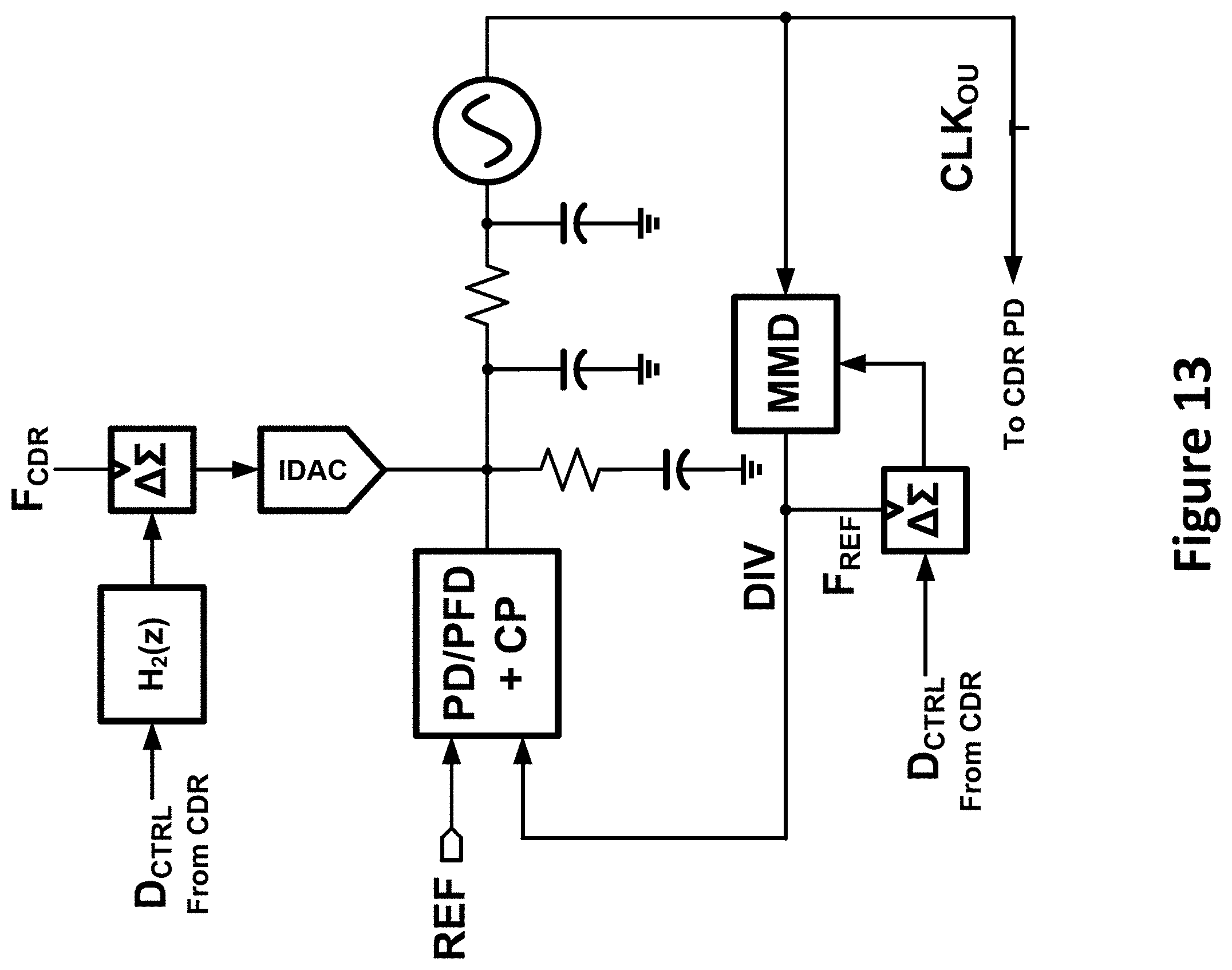
[0074] This feedforward path implementation requires digital filter as well as a current mode .DELTA..SIGMA. digital-to-analog converter (IDAC). FIG. 13 is a simplified diagram illustrating a Frac-N PLL implementation with a charge pump according to embodiments of the present invention. This diagram is merely an example, which should not unduly limit the scope of the claims. One of ordinary skill in the art would recognize many variations, alternatives, and modifications. The IDAC is configured with .DELTA..SIGMA. modulator in the signal path as shown. It is to be understood while PD and CP are shown in the same block in FIG. 13, they are implemented separately.
[0075] FIG. 14 shows the simulated CDR error transfer function peaking (top) and output jitter (bottom) as function of Frac-N PLL bandwidth with charge pump in the feedforward path. It can be seen that the CDR error transfer function peaking becomes almost independent of Frac-N PLL bandwidth. This allows for choosing Frac-N PLL bandwidth that optimizes the jitter performance.
[0076] In various embodiments, a Frac-N PLL is implemented with a feed-forward VCO path as a part of a CDR device. FIG. 15 is a simplified small signal model for a Frac-N PLL with a feed-forward VCO path according to embodiments of the present invention. This diagram is merely an example, which should not unduly limit the scope of the claims. One of ordinary skill in the art would recognize many variations, alternatives, and modifications. As shown in FIG. 15, the VCO (with gain K.sub.VCO) is configured on the feedforward path. The DCO (i.e., DCO equivalent implemented with Frac-N PLL as used in a CDR) transfer function is described in Equation 11 below:
F OUT ( s ) D C T R L ( s ) = F R E F G ( s ) + s N n o m .alpha. I C P H L P F ( s ) H 3 ( s ) G ( s ) Equation 11 ##EQU00010##
[0077] where H.sub.LPF(s) denotes the equivalent low pass transfer function of the analog loop filter connected to charge pump output. It is to be noted that the transfer function from E.sub.Q,NTF to F.sub.OUT remains unchanged. If we choose
H 3 ( s ) = F R E F K VCO , ##EQU00011##
Equation 12 below is obtained:
F OUT ( s ) D CTRL ( s ) = F R E F Equation 12 ##EQU00012##
[0078] Since H.sub.3(s) is a constant, this feedforward path implementation requires only a .DELTA..SIGMA. digital-to-analog converter. FIG. 16 is a simplified diagram illustrating a Frac-N PLL implemented with a feed-forward VCO path according to embodiments of the present invention. This diagram is merely an example, which should not unduly limit the scope of the claims. One of ordinary skill in the art would recognize many variations, alternatives, and modifications. For example, the .DELTA..SIGMA. digital-to-analog converter can be implemented as a switching capacitor in the VCO as shown in FIG. 16. For example, a digital gain scaling factor K.sub.VFF is utilized to implement H.sub.3(s) function.
[0079] FIG. 17 shows the simulated CDR error transfer function peaking (top) and output jitter (bottom) as function of Frac-N PLL bandwidth with a VCO on the feedforward path. It can be seen that the CDR error transfer function peaking becomes almost independent of Frac-N PLL bandwidth. This allows for choosing a Frac-N PLL bandwidth that optimizes the jitter performance.
[0080] It is to be noted that a VCO contributes to Frac-N PLL feedforward gain variation. As discussed before, the feedforward gain must match with Frac-N PLL K.sub.VCO to achieve an all-pass transfer function from D.sub.CTRL to F.sub.OUT. This gain scaling is implemented in digital domain, whereas the K.sub.VCO of the analog VCO varies with process, temperature, and supply voltage. As a result, there is a mismatch between the digital gain scaling factor (K.sub.VFF) and the Frac-N PLL gain. FIG. 18 shows the effect of gain mismatch on CDR error transfer function peaking. It indicates that for optimum performance, the digital path gain K.sub.VFF needs to be calibrated to match the analog gain inside Frac-N PLL.
[0081] FIG. 19 is a simplified block diagram illustrating feedforward gain calibration for Frac-N PLL implementation of CDR according to embodiments of the present invention. This diagram is merely an example, which should not unduly limit the scope of the claims. One of ordinary skill in the art would recognize many variations, alternatives, and modifications. More specifically, the foreground calibration technique illustrated in FIG. 9 involves matching digital feedforward path gain with that of analog path. As discussed above, the gain in the feedforward path (e.g., the H.sub.VFF(s) function) is to be matched with the gain Frac-N PLL path (e.g., the H.sub.FRAC(s) function).
[0082] FIG. 20 shows transfer functions for each of the two paths. It is to be noted that signal injected in Frac-N PLL path at frequency F.sub.2 has the same gain compared to the signal injected at frequency F.sub.1 in the feedforward path. Variables F.sub.CDR and F.sub.PLL denote the bandwidths for CDR and Frac-N PLL respectively. To measure the output because of the injected signal, we utilize the CDR phase detector. Since the CDR phase detector provides digital output, it can be measured in-situ.
[0083] FIG. 21 is a simplified diagram illustrating a feedforward configuration with injected signals according to embodiments of the present invention. This diagram is merely an example, which should not unduly limit the scope of the claims. One of ordinary skill in the art would recognize many variations, alternatives, and modifications. Digital square wave signals are injected through each path, and they create triangular signals at the CDR phase detector output. By detecting the peak-to-peak value of the triangular waveforms digitally, we can find the gain mismatch and correct for it by digitally adjusting K.sub.VFF. FIG. 22 provides simulation results of a feedforward implementation according to embodiments of the present invention. As an example, it shows that for an expected ratio 10 for peak to peak values, K.sub.VFF path gain needs to match with Frac-N PLL path gain. For other scaling factors the ratio of peak-to-peak values deviates from 10.
[0084] It is to be appreciated that Frac-N PLLs can be implemented into CDR devices in various ways. For example, the combination and configuration of charge pump, VCO, and/or other components of a Frac-N PLL can be used to allow the Frac-N PLL to satisfy the requirements of CDR devices.
[0085] While the above is a full description of the specific embodiments, various modifications, alternative constructions and equivalents may be used. Therefore, the above description and illustrations should not be taken as limiting the scope of the present invention which is defined by the appended claims.
* * * * *
D00000
D00001
D00002
D00003
D00004
D00005
D00006
D00007
D00008
D00009
D00010
D00011
D00012

D00013
D00014

D00015

D00016

D00017

D00018

D00019

D00020

D00021
D00022


XML
uspto.report is an independent third-party trademark research tool that is not affiliated, endorsed, or sponsored by the United States Patent and Trademark Office (USPTO) or any other governmental organization. The information provided by uspto.report is based on publicly available data at the time of writing and is intended for informational purposes only.
While we strive to provide accurate and up-to-date information, we do not guarantee the accuracy, completeness, reliability, or suitability of the information displayed on this site. The use of this site is at your own risk. Any reliance you place on such information is therefore strictly at your own risk.
All official trademark data, including owner information, should be verified by visiting the official USPTO website at www.uspto.gov. This site is not intended to replace professional legal advice and should not be used as a substitute for consulting with a legal professional who is knowledgeable about trademark law.