Transition-metal Oxides-coated Hydrogen-terminated Diamond Surface And Uses Thereof
KALISH; Rafi ; et al.
U.S. patent application number 16/644015 was filed with the patent office on 2020-12-24 for transition-metal oxides-coated hydrogen-terminated diamond surface and uses thereof. This patent application is currently assigned to Technion Research & Development Foundation Ltd.. The applicant listed for this patent is TECHNION RESEARCH & DEVELOPMENT FOUNDATION LTD.. Invention is credited to Rafi KALISH, Moshe TORDJMAN.
| Application Number | 20200403067 16/644015 |
| Document ID | / |
| Family ID | 1000005130362 |
| Filed Date | 2020-12-24 |


View All Diagrams
| United States Patent Application | 20200403067 |
| Kind Code | A1 |
| KALISH; Rafi ; et al. | December 24, 2020 |
TRANSITION-METAL OXIDES-COATED HYDROGEN-TERMINATED DIAMOND SURFACE AND USES THEREOF
Abstract
The present invention provides a conducting material comprising a carbon-based material selected from a diamond or an insulating diamond-like carbon, having a hydrogen-terminated surface and a layer of tungsten trioxide, rhenium trioxide, or chromium oxide coating said hydrogen-terminated surface. Such conducting materials are useful in the fabrication of electronic components, electrodes, sensors, diodes, field effect transistors, and field emission electron sources.
| Inventors: | KALISH; Rafi; (Haifa, IL) ; TORDJMAN; Moshe; (Haifa, IL) | ||||||||||
| Applicant: |
|
||||||||||
|---|---|---|---|---|---|---|---|---|---|---|---|
| Assignee: | Technion Research & Development
Foundation Ltd. Technion City, Haifa IL |
||||||||||
| Family ID: | 1000005130362 | ||||||||||
| Appl. No.: | 16/644015 | ||||||||||
| Filed: | September 2, 2018 | ||||||||||
| PCT Filed: | September 2, 2018 | ||||||||||
| PCT NO: | PCT/IL2018/050971 | ||||||||||
| 371 Date: | March 3, 2020 |
Related U.S. Patent Documents
| Application Number | Filing Date | Patent Number | ||
|---|---|---|---|---|
| 62553871 | Sep 3, 2017 | |||
| Current U.S. Class: | 1/1 |
| Current CPC Class: | H01B 1/04 20130101; H01L 29/872 20130101; H01L 29/7786 20130101; H01J 37/073 20130101; H01B 1/08 20130101; H01L 29/167 20130101; H01L 29/1602 20130101 |
| International Class: | H01L 29/16 20060101 H01L029/16; H01B 1/04 20060101 H01B001/04; H01B 1/08 20060101 H01B001/08; H01J 37/073 20060101 H01J037/073; H01L 29/778 20060101 H01L029/778; H01L 29/872 20060101 H01L029/872; H01L 29/167 20060101 H01L029/167 |
Claims
1. A conducting material comprising a carbon-based material selected from a diamond or insulating diamond-like carbon, having a hydrogen-terminated surface and a layer of tungsten trioxide (WO.sub.3), rhenium trioxide (ReO.sub.3), or chromium oxide (CrO.sub.3) coating said hydrogen-terminated surface.
2. The conducting material of claim 1, wherein said diamond is polycrystalline diamond, nanocrystalline diamond, ultra-nanocrystalline diamond, or single diamond.
3. The conducting material of claim 1, having a tungsten trioxide layer coating said hydrogen-terminated surface.
4. The conducting material of claim 3, wherein said tungsten trioxide layer is a single- or multi-layer of tungsten trioxide having a thickness in a range of 5 .ANG. to 1000 .ANG..
5. The conducting material of claim 1, having a rhenium trioxide layer coating said hydrogen-terminated surface.
6. The conducting material of claim 5, wherein said rhenium trioxide layer is a single- or multi-layer of rhenium trioxide having a thickness in a range of 5 .ANG. to 1000 .ANG..
7. The conducting material of claim 1, having a chromium oxide layer coating said hydrogen-terminated surface.
8. The conducting material of claim 7, wherein said chromium oxide layer is a single- or multi-layer of chromium oxide having a thickness in a range of 5 .ANG. to 1000 .ANG..
9. The conducting material of claim 1, wherein said carbon-based material is diamond and the thickness of said tungsten trioxide layer is in a range of 5 .ANG. to 1000 .ANG..
10. The conducting material of claim 9, having (i) an electrical stability of up to 300.degree. C., or (ii) a sheet conductance higher than 10.sup.-5.OMEGA..sup.-1, and a hole carrier concentration higher than 10.sup.11 cm.sup.-2.
11. (canceled)
12. The conducting material of claim 10, having a sheet conductance in a range of 10.sup.-5.OMEGA..sup.-1 to 10.sup.-2.OMEGA..sup.-1, and a hole carrier concentration in a range of 10.sup.11 cm.sup.-2 to 3.times.10.sup.14 cm.sup.-2.
13. The conducting material of claim 1, wherein said carbon-based material is diamond and the thickness of said rhenium trioxide layer is in a range of 5 .ANG. to 1000 .ANG..
14. The conducting material of claim 13, having (i) an electrical stability of up to at least 450.degree. C., or (ii) a sheet conductance higher than 10.sup.-5.OMEGA..sup.-1, and a hole carrier concentration higher than 10.sup.12 cm.sup.-2.
15. (canceled)
16. The conducting material of claim 4544, having a sheet conductance in a range of 10.sup.-5.OMEGA..sup.-1 to 10.sup.-2.OMEGA..sup.-1, and a hole carrier concentration in a range of 10.sup.12 cm.sup.-2 to 10.sup.14 cm.sup.-2.
17. The conducting material of claim 1, wherein said carbon-based material is diamond and the thickness of said chromium oxide layer is in a range of 5 .ANG. to 1000 .ANG..
18. The conducting material of claim 17, having (i) an electrical stability of up to at least 450.degree. C., or (ii) a sheet conductance higher than 10.sup.-5.OMEGA..sup.-1, and a hole carrier concentration higher than 10.sup.12 cm.sup.-2.
19. (canceled)
20. The conducting material of claim 4918, having a sheet conductance in a range of 10.sup.-5.OMEGA..sup.-1 to 10.sup.-2.OMEGA..sup.-1, and a hole carrier concentration in a range of 10.sup.12 cm.sup.-2 to 10.sup.14 cm.sup.-2.
21. An electronic component comprising a conducting material according to claim 1.
22. An electrode comprising a conducting material according to claim 1.
23. The electrode of claim 23, comprising said conducting material as a conductive layer.
24. A sensor comprising a conducting material according to claim 1.
25. In a method for detection of a chemical or biological material using a sensor, the improvement wherein said sensor comprises a conducting material according to claim 1.
26. A diode comprising a conducting material according to claim 1.
27. The diode of claim 26, comprising a p-n junction, a p-n-p heterojunction or n-p-n heterojunction, wherein one or more of the p-type layers comprises said conducting material and/or said conducting material bridges said p-n junction, p-n-p heterojunction or n-p-n heterojunction, or configured as a schottky diode.
28. (canceled)
29. A field effect transistor (FET) comprising a conductive material according to claim 1, as either a conductive layer or a p-type layer.
30. The FET of claim 29, constructed as a high-frequency high power FET.
31. A field emission electron source comprising a conductive material according to claim 1.
Description
TECHNICAL FIELD
[0001] The present invention relates to a conductive diamond surface, more particularly to tungsten trioxide (WO.sub.3), rhenium trioxide (ReO.sub.3), or chromium oxide (CrO.sub.3)-coated hydrogen-terminated diamond surface showing thermal stability with superior sheet conductivity and hole carrier concentration, and to uses thereof.
BACKGROUND ART
[0002] The next-generation of outperforming electronic devices is predicted to be led by diamond implementation as extreme semiconductors, as they have the most favorable properties among other semiconductors for this task (i.e., highest breakdown field and thermal conductivity, dielectric constant, and carrier transport properties). Up to date, due to the lack of suitable bulk dopants (acceptors and donors) with low activation energies (Kalish, 2007), diamond free carriers are found only at the surface and are generated by an unique sub-surface two-dimensional hole gas (2DHG) (Strobel et al., 2004; Chakrapani et al., 2007). This 2DHG is formed by an upward band bending (BB), following electron charge transfer from a hydrogen-terminated diamond (diamond:H) valence band maximum (VBM) to a lower unoccupied state of a surface electron acceptor (i.e., >4.2 eV from vacuum level). This induced p-type surface conductivity has first been seen in air-exposed hydrogen-terminated diamond (Landstrass and Ravi, 1989) and has been modeled by an electrochemical charge-exchange at the interface called transfer doping (TD) (Maier et al., 2000).
[0003] This elementary air-exposed surface TD has opened-up initial realization of diamond-based electronic devices (Umezawa et al., 1999; Taniuchi et al., 2001; Kasu et al., 2005; Kasu et al., 2007), nanoscale planar doped electronic devices (Sussmann, 2009; Geisler and Hugel, 2010), electrochemical electrodes (Poh et al., 2004; Christiaens et al., 2006), and biological electrodes sensors (Yang et al., 2002; Lud et al., 2006; Dankerl et al., 2011), to name just a few. In light of this wide spectrum of promising applications, a lot of efforts are invested for recognizing new surface electron acceptors with ability to surpass existing fragile surface TD of diamond:H. Among all the exposed surface acceptor candidates studied so far, none have yet offered a satisfactory and robust solution for assuring sustainability and efficiency of the diamond surface conductivity as they are required for practical electronic device processing and reliability.
[0004] First attempts to improve aqueous (i.e., H.sub.2O) air-exposed diamond:H conductivity performances (Sauerer et al., 2001) involved the use of alternative adsorbate molecules with high electron affinity (Strobel et al., 2006; Qi et al., 2007). Nevertheless, all those proposed surface electron acceptor molecules were still suffering from instability to temperature fluctuations, resulting in loss of conductivity upon heating (Laikhtman et al., 2004). Thus, the critical need to find more stable and efficient surface acceptor substitutes.
[0005] A second approach proposes to encapsulate the above fragile surface acceptors with thick oxide layers (i.e., Al.sub.2O.sub.3) in order to protect the first active electron acceptor adsorbates on the diamond:H surface (i.e., induced by air) (Kawarada, 2014; Daicho et al., 2014). It has been further developed by using thick capsuling oxide layers (100 nm) with high work functions (e.g., Nb.sub.2O.sub.5, WO.sub.3, V.sub.2O.sub.5, MoO.sub.3 vs. Al.sub.2O.sub.3) in order to exploit them as additional active layers over the air-doped diamond:H surface (Verona et al., 2016). A recent AlN capping layer work has achieved a hole carrier concentration value of 1.times.10.sup.14 cm.sup.-2 using H.sub.2+NH.sub.3 (Imura et al., 2017) activation of diamond:H, and comparable values from 8.2.times.10.sup.13 cm.sup.-2 to 1.7.times.10.sup.14 cm.sup.-2 have been reported for a NO.sub.2 activation (Wade et al., 2017; Sato and Kasu, 2013). However, despite the ameliorations, all the above approaches have considerable limitation such as in the design, process, and architecture of diamond:H-based electronic devices because the resulting 2DHG conductive channel must be protected with an additional impeding capsulation layer.
[0006] Recent advances were reported in the surface TD of diamond:H, using uniquely transition-metal oxides with high work functions as direct exposed surface electron acceptors (without capping), such as MoO.sub.3 (.phi.=5.6-6.8 eV) and V.sub.2O.sub.5 (.phi.=7 eV) (Russell et al., 2013; Tordjman et al., 2014; Crawford et al., 2016). In these cases, diamond:H/MoO.sub.3 (Tordjman et al., 2014) demonstrated a hole carrier concentration up to 1.times.10.sup.14 cm.sup.-2, and diamond:H/V.sub.2O.sub.5 (Tordjman et al., 2014) displayed values comparable to those of air-exposed diamond:H (Sauerer et al., 2001) (e.g., 1.8.times.10.sup.13 cm.sup.-2) but with a thermal stability of up to 300.degree. C. In both cases, oxygen deficiency upon exposure to air is critical and degrades their original efficient work function (Irfan et al., 2012; Greiner et al., 2012). Consequently, the first active monolayer has to be buried with additional protecting layers (e.g. 50 .ANG. for MoO.sub.3 and 100 .ANG. for V.sub.2O.sub.5) in order to overcome this lacunae. Hence, the crucial need is to find alternative candidates with higher efficiency and thermal stability at the very first monolayer of coverage. Such a desirable case will ensure the close proximity of electrical top-contacts to the sub-surface 2DHG conductive channel (rich in carrier concentration) and will cancel the need for additional encumbering protective layers.
SUMMARY OF INVENTION
[0007] In one aspect, the present invention provides a conducting material comprising a carbon-based material selected from a diamond or insulating diamond-like carbon, having a hydrogen-terminated surface and a layer of tungsten trioxide (WO.sub.3), rhenium trioxide (ReO.sub.3), or chromium oxide (CrO.sub.3) coating said hydrogen-terminated surface.
[0008] In another aspect, the present invention relates to an electronic component comprising a conducting material as defined above, i.e., a conducting material comprising a carbon-based material having a hydrogen-terminated surface and a layer of WO.sub.3, ReO.sub.3, or CrO.sub.3 coating said hydrogen-terminated surface.
[0009] In still another aspect, the present invention relates to an electrode comprising a conducting material as defined above, i.e., a conducting material comprising a carbon-based material having a hydrogen-terminated surface and a layer of WO.sub.3, ReO.sub.3, or CrO.sub.3 coating said hydrogen-terminated surface.
[0010] In yet another aspect, the present invention relates to a sensor comprising a conducting material as defined above, i.e., a conducting material comprising a carbon-based material having a hydrogen-terminated surface and a layer of WO.sub.3, ReO.sub.3, or CrO.sub.3 coating said hydrogen-terminated surface. Such sensors can be used for detecting chemical and biological materials. In still other aspects, the present invention thus relates to the use of such a sensor for the detection of a chemical or biological material; and to a method for the detection of a chemical or biological material utilizing said sensor.
[0011] In another aspect, the present invention relates to a diode comprising a conducting material as defined above, i.e., a conducting material comprising a carbon-based material having a hydrogen-terminated surface and a layer of WO.sub.3, ReO.sub.3, or CrO.sub.3 coating said hydrogen-terminated surface.
[0012] In still another aspect, the present invention relates to a FET comprising a conducting material as defined above, i.e., a conducting material comprising a carbon-based material having a hydrogen-terminated surface and a layer of WO.sub.3, ReO.sub.3, or CrO.sub.3 coating said hydrogen-terminated surface.
[0013] In yet another aspect, the present invention relates to a field emission electron source, e.g., a field emission cold cathode, comprising a conducting material as defined above, i.e., a conducting material comprising a carbon-based material having a hydrogen-terminated surface and a layer of WO.sub.3, ReO.sub.3, or CrO.sub.3 coating said hydrogen-terminated surface.
BRIEF DESCRIPTION OF DRAWINGS
[0014] FIG. 1 shows sheet hole carrier concentration as measured (under identical conditions) by Hall effect of transfer doped hydrogen terminated diamond with ReO.sub.3 and WO.sub.3, as a function of incremental surface acceptor thickness coverage, and H.sub.2O-air-exposed (sphere) result presented as reference. (Inset) Transfer doping efficiency vs. surface acceptor thickness at close diamond interface proximity for each respective transition-metal oxide.
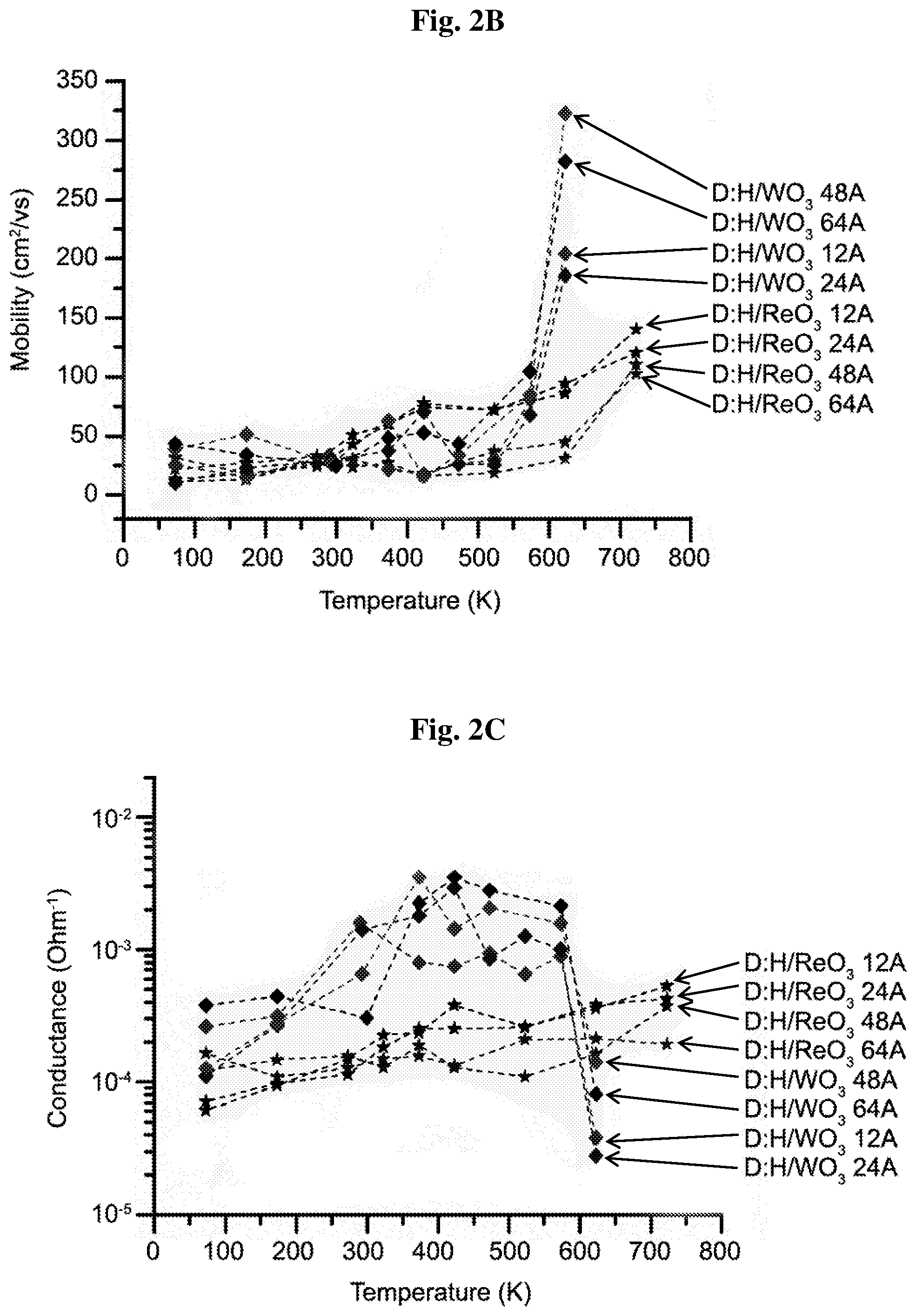
[0015] FIGS. 2A-2C show sheet hole carrier concentration (2A); mobility (2B); and conductance (2C) of transfer doped hydrogen terminated diamond samples with ReO.sub.3 and WO.sub.3 for different thicknesses as function of temperature (K).
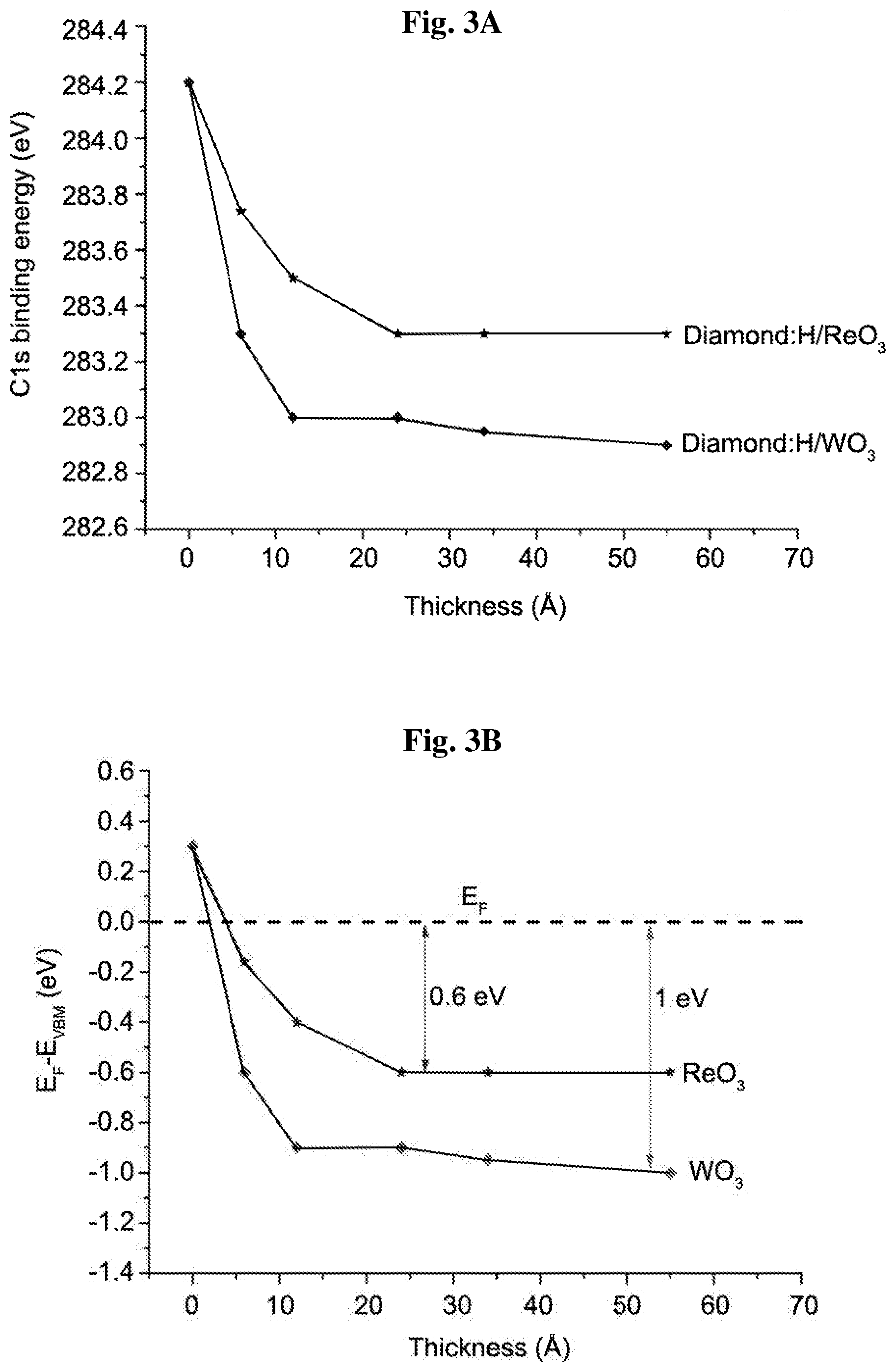
[0016] FIGS. 3A-3D show C1s diamond bulk binding energy position as a function of incremental ReO.sub.3 and WO.sub.3 films thicknesses (6 .ANG. to 45 .ANG.) deposited on hydrogenated diamond (3A); variation of E.sub.F-E.sub.VBM values as a function of ReO.sub.3 and WO.sub.3 thickness coverage derived from XPS measurement of C1s diamond bulk binding energy position (3B); and the Re4f and W4f XPS spectra plots of the respective deposited ReO.sub.3 and WO.sub.3 film thicknesses showing the Re.sup.6+ and W.sup.6+ oxidation state structures represented in dotted lines vs. a continuous line for raw data (3C and 3D, respectively).
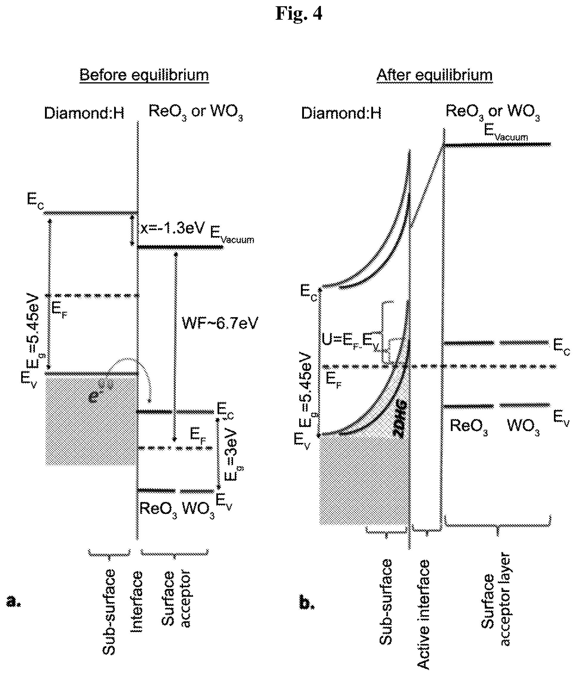
[0017] FIG. 4 schematically illustrates the energy-level diagram before charge exchange (left) and after equilibrium (right) of the surface transfer doping of hydrogenated diamond with ReO.sub.3 and WO.sub.3. A modified 2DHG depth-lying is illustrated following the corresponding band bending values and different transfer-doping efficiency of ReO.sub.3 and WO.sub.3.
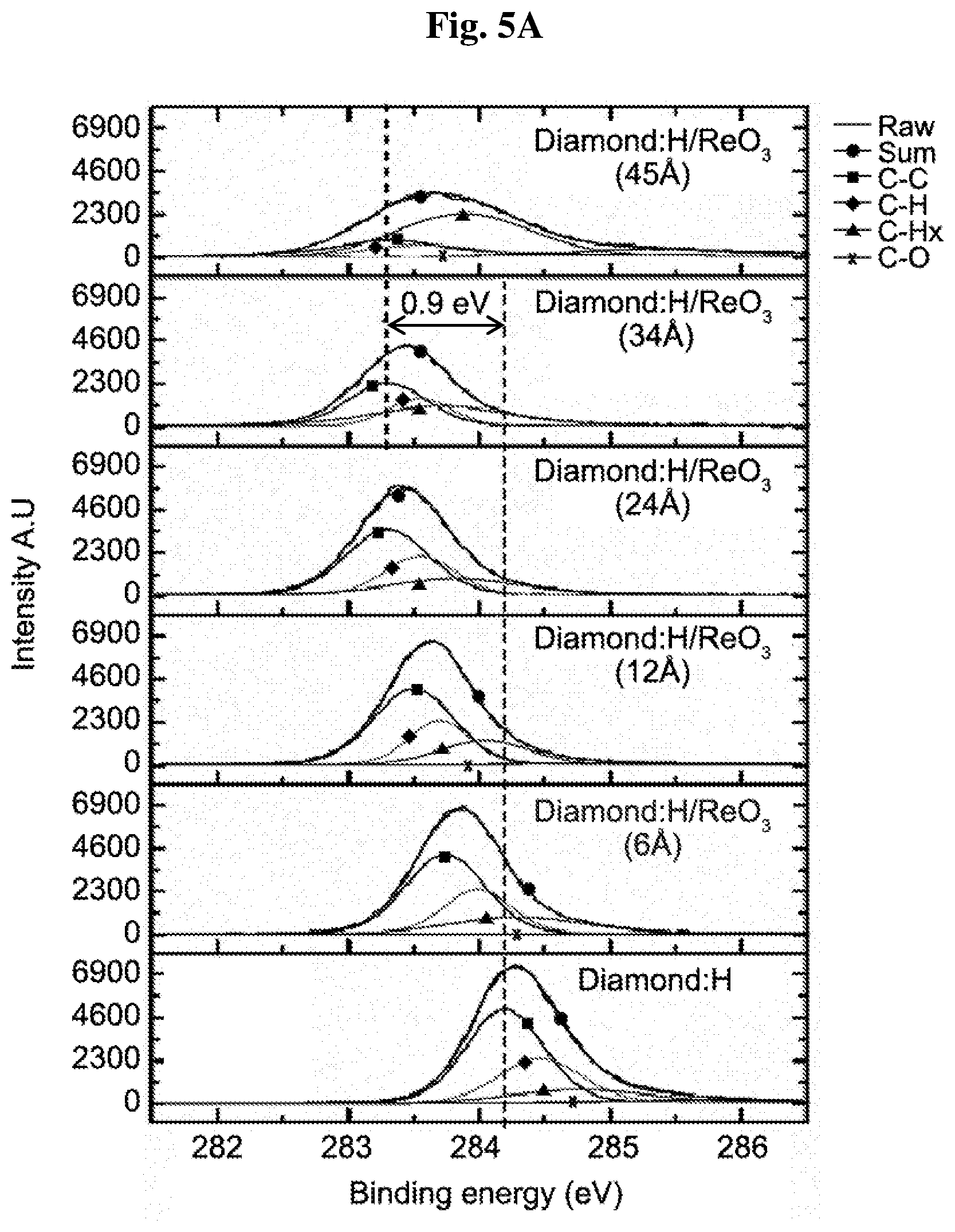
[0018] FIGS. 5A-5B show C1s XPS spectra for incremental ReO.sub.3 (5A) and WO.sub.3 (5B) films thicknesses (6 .ANG. to 45 .ANG.) deposited on hydrogenated diamond. Marked are: C--C bonds from bulk diamond component, the surface component C--H, a surface component contaminant hydrocarbon C--H, carboxyl weak feature C--O, sum of fitted peaks (black dots) and (gray line) experimental data (almost overlapping).
[0019] FIG. 6 shows a schematic cross-section of starting heterostructure (left) and p-type diamond:H/WO.sub.3 MOSFET (right).
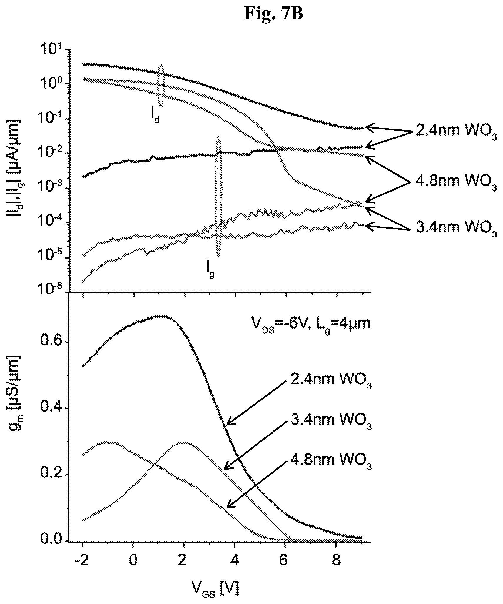
[0020] FIGS. 7A-7B show output (7A) and transfer (7B) characteristics for L.sub.g=4 diamond:H/WO.sub.3 FETs with WO.sub.3 thickness ranging from 2.4 nm to 4.8 nm.
[0021] FIGS. 8A-8D show electrical characteristics of 4.8 nm-thick WO.sub.3 diamond:H/WO.sub.3 FETs with gate width of 20 .mu.m and different gate lengths ranging from 0.7 .mu.m to 5 .mu.m: (8A) subthreshold and gate current characteristics; (8B) g.sub.m characteristics; (8C) maximum g.sub.m (g.sub.mmax) and maximum drain current (I.sub.Dsat), all at V.sub.DS=-6 V; (8D) ON resistance.
[0022] FIGS. 9A-9B show output (9A) and transfer (9B) characteristics for L.sub.g=5 .mu.m WO.sub.3=4.8 nm diamond:H/WO.sub.3 FETs measured at 77 K and room temperature (RT).
[0023] FIG. 10 shows split C-V measurements at 1 MHz of a typical diamond:HAVO3 FET (L.sub.g=5 .mu.m, W.sub.g=20 .mu.m, WO.sub.3=4.8 nm) at 77 K. Inset: sheet hole mobility vs. sheet hole concentration.
DETAILED DESCRIPTION
[0024] It has now been found, in accordance with the present invention, that an advanced charge-transfer yield is demonstrated by employing single monolayers of the transition-metal oxides WO.sub.3 and ReO.sub.3 deposited on hydrogenated diamond surface, resulting in improved p-type sheet conductivity and thermal stability. Surface conductivities, as determined by Hall effect measurements as function of temperature for WO.sub.3 yield a record sheet hole carrier concentration value up to 2.52.times.10.sup.14 cm.sup.-2 at room temperature for only few monolayers of coverage. Transfer doping with ReO.sub.3 exhibits a consistent narrow sheet carrier concentration range value of around 3.times.10.sup.13 cm.sup.-2, exhibiting thermal stability up to 450.degree. C. These enhanced conductivity and temperature robustness exceed those reported for previous exposed surface electron acceptor materials used so far on diamond surface. X-ray photoelectron spectroscopy (XPS) measurements of the C1s core level shift as function of WO.sub.3 and ReO.sub.3 layer thicknesses are used to determine the respective increase in surface band bending of the accumulation layers, leading to a different sub-surface two-dimensional hole gas formation efficiency in both cases. This substantial difference in charge-exchange efficiency is unexpected since both surface acceptors have very close work functions values. Transfer doping with WO.sub.3 reveals the highest yet reported transfer doping efficiency per minimal surface acceptor coverage. This improved surface conductivity performance and thermal stability will promote the realization of 2D diamond-based electronic devices facing process fabrication challenges.
[0025] In one aspect, the present invention thus provides a conducting material comprising a carbon-based material selected from a diamond or insulating diamond-like carbon, having a hydrogen-terminated surface and a layer of tungsten trioxide (WO.sub.3), rhenium trioxide (ReO.sub.3), or chromium oxide (CrO.sub.3) coating said hydrogen-terminated surface.
[0026] The term "diamond" refers to a carbon-based material which is almost always found in the crystalline form with a purely cubic orientation of spa bonded carbon atoms, i.e., to a carbon-based material in which each carbon atom is covalently bonded to four other carbon atoms in a tetrahedron. Particular diamonds include polycrystalline diamonds, nanocrystalline diamonds, ultra-nanocrystalline diamonds, and homoepitaxial single diamonds, each optionally doped by boron, nitrogen, hydrogen, phosphorus, or a combination thereof. In certain embodiments, the diamond is a homoepitaxial single crystal diamond, particularly an undoped homoepitaxial single crystal diamond type IIa.
[0027] The term "diamond-like carbon" as used herein refers to an amorphous carbon phase having sp.sup.3 hybridized bonds as well as a certain amount of sp.sup.2 hybridized bonds, more particularly, a material that has high sp.sup.3 hybridized bonds content and displays some of the physical properties of diamond. Diamond-like carbons exist in seven different forms of amorphous carbon materials, all containing significant amounts of sp.sup.3 hybridized carbon atoms. The different forms of diamond-like carbons may be produced by mixing the two crystalline polytypes of diamond, i.e., the one having a cubic lattice and the other rare one having a hexagonal lattice, in various ways at the nanoscale level of structure, and these materials may therefore be at the same time amorphous, flexible, and yet purely sp.sup.3 bonded "diamond". The hardest, strongest, and slickest mixture is that known as tetrahedral amorphous carbon, or ta-C, considered to be the "pure" form of diamond-like carbon, as it consists of sp.sup.3 bonded carbon atoms only. Diamond-like carbons close enough to ta-C on plots of bonding ratios and hydrogen content can be insulators with high values of resistivity. The term "insulating diamond-like carbon" as used herein thus refers to a diamond-like carbon having about 50% or more, e.g., about 50%, 55%, 60%, 65%, 70% 75%, 80%, 85%, 90%, 95% or more, sp.sup.3 hybridized bonds. It should be noted that where particular values are described in the description and claims, unless otherwise stated, the term "about" means that an acceptable error range, e.g., up to 5% or 10%, for the particular value should be assumed.
[0028] In a particular such aspect, the present invention provides a conducting material comprising a diamond having a hydrogen-terminated surface and a layer of WO.sub.3, ReO.sub.3, or CrO.sub.3 coating said surface, wherein said diamond may be a polycrystalline diamond, nanocrystalline diamond, ultra-nanocrystalline diamond, or homoepitaxial single diamond, undoped or doped by boron, nitrogen, hydrogen, phosphorus, or a combination thereof, e.g., an undoped homoepitaxial single crystal diamond type IIa.
[0029] In certain embodiments, the WO.sub.3, ReO.sub.3 or CrO.sub.3 layer coating the hydrogen-terminated surface of the carbon-based material is a single-layer or a multi-layer of said oxide having a thickness in a range of 5 .ANG. to 1000 .ANG., 5 .ANG. to 900 .ANG., 5 .ANG. to 800 .ANG., 5 .ANG. to 700 .ANG., 5 .ANG. to 600 .ANG., 5 .ANG. to 500 .ANG., 5 .ANG. to 450 .ANG., 5 .ANG. to 400 .ANG., 5 .ANG. to 350 .ANG., 5 .ANG. to 300 .ANG., 5 .ANG. to 250 .ANG., 5 .ANG. to 200 .ANG., 5 .ANG. to 150 .ANG., or 5 .ANG. to 100 .ANG..
[0030] In some embodiments, the conducting material of the invention comprises a carbon-based material selected from a diamond or insulating diamond-like carbon, having a hydrogen-terminated surface and a layer of WO.sub.3 coating said hydrogen-terminated surface. In particular such embodiments, said WO.sub.3 layer is a single- or multi-layer of WO.sub.3 having a thickness in a range of 5 .ANG. to 1000 .ANG., 5 .ANG. to 900 .ANG., 5 .ANG. to 800 .ANG., 5 .ANG. to 700 .ANG., 5 .ANG. to 600 .ANG., 5 .ANG. to 500 .ANG., 5 .ANG. to 450 .ANG., 5 .ANG. to 400 .ANG., 5 .ANG. to 350 .ANG., 5 .ANG. to 300 .ANG., 5 .ANG. to 250 .ANG., 5 .ANG. to 200 .ANG., 5 .ANG. to 150 .ANG., or 5 .ANG. to 100 .ANG.. Preferred such embodiments are those wherein said WO.sub.3 layer has a thickness in the range of 5 .ANG. to 150 .ANG., or 5 .ANG. to 100 .ANG..
[0031] In other embodiments, the invention provides a conducting material comprising a carbon-based material selected from a diamond or insulating diamond-like carbon, having a hydrogen-terminated surface and a layer of ReO.sub.3 coating said hydrogen-terminated surface. In particular such embodiments, said ReO.sub.3 layer is a single- or multi-layer of ReO.sub.3 having a thickness in a range of 5 .ANG. to 1000 .ANG., 5 .ANG. to 900 .ANG., 5 .ANG. to 800 .ANG., 5 .ANG. to 700 .ANG., 5 .ANG. to 600 .ANG., 5 .ANG. to 500 .ANG., 5 .ANG. to 450 .ANG., 5 .ANG. to 400 .ANG., 5 .ANG. to 350 .ANG., 5 .ANG. to 300 .ANG., 5 .ANG. to 250 .ANG., 5 .ANG. to 200 .ANG., 5 .ANG. to 150 .ANG., or 5 .ANG. to 100 .ANG.. Preferred embodiments are those wherein said ReO.sub.3 layer has a thickness in the range of 5 .ANG. to 150 .ANG., or 5 .ANG. to 100 .ANG..
[0032] In further embodiments, the invention provides a conducting material comprising a carbon-based material selected from a diamond or insulating diamond-like carbon, having a hydrogen-terminated surface and a layer of CrO.sub.3 coating said hydrogen-terminated surface. In particular such embodiments, said CrO.sub.3 layer is a single- or multi-layer of CrO.sub.3 having a thickness in a range of 5 .ANG. to 1000 .ANG., 5 .ANG. to 900 .ANG., 5 .ANG. to 800 .ANG., 5 .ANG. to 700 .ANG., 5 .ANG. to 600 .ANG., 5 .ANG. to 500 .ANG., 5 .ANG. to 450 .ANG., 5 .ANG. to 400 .ANG., 5 .ANG. to 350 .ANG., 5 .ANG. to 300 .ANG., 5 .ANG. to 250 .ANG., 5 .ANG. to 200 .ANG., 5 .ANG. to 150 .ANG., or 5 .ANG. to 100 .ANG.. Preferred embodiments are those wherein said CrO.sub.3 layer has a thickness in the range of 5 .ANG. to 150 .ANG., or 5 .ANG. to 100 .ANG..
[0033] In certain embodiments, the carbon based material composing the conducting material of the present invention is a diamond, in any one of the forms listed above, and the thickness of the WO.sub.3 layer coating the hydrogen-terminated surface of the diamond is in a range of 5 .ANG. to 1000 .ANG., 5 .ANG. to 900 .ANG., 5 .ANG. to 800 .ANG., 5 .ANG. to 700 .ANG., 5 .ANG. to 600 .ANG., 5 .ANG. to 500 .ANG., 5 .ANG. to 450 .ANG., 5 .ANG. to 400 .ANG., 5 .ANG. to 350 .ANG., 5 .ANG. to 300 .ANG., 5 .ANG. to 250 .ANG., 5 .ANG. to 200 .ANG., 5 .ANG. to 150 .ANG., or 5 .ANG. to 100 .ANG., but preferably in the range of 5 .ANG. to 150 .ANG., or 5 .ANG. to 100 .ANG.. As shown herein, such conducting materials have an electrical stability of up to 300.degree. C. In particular such embodiments, the conducting material of the invention has a sheet conductance higher than 1.times.10.sup.-5.OMEGA..sup.-1, e.g., in a range of 10.sup.-5.OMEGA..sup.-1 to 10.sup.-2.OMEGA..sup.-1; and a hole carrier concentration higher than 1.times.10.sup.11 cm.sup.-2, with thickness and temperature dependency, or higher than 10.sup.13 cm.sup.-2 at room temperature, e.g., in a range of 10.sup.11 cm.sup.-2 to 3.times.10.sup.14 cm.sup.-2.
[0034] In certain embodiments, the carbon based material composing the conducting material of the present invention is a diamond, in any one of the forms listed above, and the thickness of the ReO.sub.3 layer coating the hydrogen-terminated surface of the diamond is in a range of 5 .ANG. to 1000 .ANG., 5 .ANG. to 900 .ANG., 5 .ANG. to 800 .ANG., 5 .ANG. to 700 .ANG., 5 .ANG. to 600 .ANG., 5 .ANG. to 500 .ANG., 5 .ANG. to 450 .ANG., 5 .ANG. to 400 .ANG., 5 .ANG. to 350 .ANG., 5 .ANG. to 300 .ANG., 5 .ANG. to 250 .ANG., 5 .ANG. to 200 .ANG., 5 .ANG. to 150 .ANG., or 5 .ANG. to 100 .ANG., but preferably in the range of 5 .ANG. to 150 .ANG., or 5 .ANG. to 100 .ANG.. As shown herein, such conducting materials have an electrical stability of up to 450.degree. C. In particular such embodiments, the conducting material of the invention has a sheet conductance higher than 1.times.10.sup.-5.OMEGA..sup.-1, e.g., in a range of 10.sup.-5.OMEGA..sup.-1 to 10.sup.-2.OMEGA..sup.-1; and a hole carrier concentration higher than 10.sup.12 cm.sup.-2, with thickness and temperature dependency, or higher than 10.sup.13 cm.sup.-2 at room temperature, e.g., in a range of 10.sup.12 cm.sup.-2 to 10.sup.14 cm.sup.-2.
[0035] In certain embodiments, the carbon based material composing the conducting material of the present invention is a diamond, in any one of the forms listed above, and the thickness of the CrO.sub.3 layer coating the hydrogen-terminated surface of the diamond is in a range of 5 .ANG. to 1000 .ANG., 5 .ANG. to 900 .ANG., 5 .ANG. to 800 .ANG., 5 .ANG. to 700 .ANG., 5 .ANG. to 600 .ANG., 5 .ANG. to 500 .ANG., 5 .ANG. to 450 .ANG., 5 .ANG. to 400 .ANG., 5 .ANG. to 350 .ANG., 5 .ANG. to 300 .ANG., 5 .ANG. to 250 .ANG., 5 .ANG. to 200 .ANG., 5 .ANG. to 150 .ANG., or 5 .ANG. to imA, but preferably in the range of 5 .ANG. to 150 .ANG., or 5 .ANG. to 100 .ANG.. Such conducting materials have an electrical stability of up to 450.degree. C. In particular such embodiments, the conducting material of the invention has a sheet conductance higher than 1.times.10.sup.-5.OMEGA..sup.-1, e.g., in a range of 10.sup.-5.OMEGA..sup.-1 to 10.sup.-2.OMEGA..sup.-1; and a hole carrier concentration higher than 10.sup.12 cm.sup.-2, with thickness and temperature dependency, or higher than 10.sup.13 cm.sup.-2 at room temperature, e.g., in a range of 10.sup.12 cm.sup.-2 to 10.sup.14 cm.sup.-2.
[0036] In another aspect, the present invention relates to an electronic component comprising a conducting material as defined in any one of the embodiments above, i.e., a conducting material comprising a carbon-based material having a hydrogen-terminated surface and a layer of WO.sub.3, ReO.sub.3, or CrO.sub.3 coating said hydrogen-terminated surface. In certain embodiments, the electronic component of the invention comprises a conducting material wherein the carbon-based material is a diamond in any one of the forms listed above, and the thickness of the oxide layer coating the hydrogen-terminated surface of the diamond is in a range of 5 .ANG. to 1000 .ANG., but preferably 5 .ANG. to 150 .ANG., or 5 .ANG. to 100 .ANG.. Particular such electronic components are those wherein said diamond is coated with (i) a WO.sub.3 layer having a thickness in a range of 5 .ANG. to 1000 .ANG., wherein said conducting material has a sheet conductance higher than 1.times.10.sup.-5.OMEGA..sup.-1, e.g., in a range of 10.sup.-5.OMEGA..sup.-1 to 10.sup.-2.OMEGA..sup.-1, and a hole carrier concentration higher than 1.times.10.sup.11 cm.sup.-2, e.g., in a range of 10.sup.11 cm.sup.-2 to 3.times.10.sup.14 cm.sup.-2; (ii) a ReO.sub.3 layer having a thickness in a range of 5 .ANG. to 1000 .ANG., wherein said conducting material has a sheet conductance higher than 1.times.10.sup.-5.OMEGA..sup.-1, e.g., in a range of 10.sup.-5.OMEGA..sup.-1 to 10.sup.-2.OMEGA..sup.-1, and a hole carrier concentration higher than 10.sup.12 cm.sup.-2, e.g., in a range of 10.sup.12 cm.sup.-2 to 10.sup.14 cm.sup.-2; or (iii) a CrO.sub.3 layer having a thickness in a range of 5 .ANG. to 1000 .ANG., wherein said conducting material has a sheet conductance higher than 1.times.10.sup.-5.OMEGA..sup.-1, e.g., in a range of 10.sup.-5.OMEGA..sup.-1 to 10.sup.-2.OMEGA..sup.-1, and a hole carrier concentration higher than 10.sup.12 cm.sup.-2, e.g., in a range of 10.sup.12 cm.sup.-2 to 10.sup.14 cm.sup.-2.
[0037] In still another aspect, the present invention relates to an electrode comprising a conducting material as defined in any one of the embodiments above, i.e., a conducting material comprising a carbon-based material having a hydrogen-terminated surface and a layer of WO.sub.3, ReO.sub.3, or CrO.sub.3 coating said hydrogen-terminated surface. In certain embodiments, the electrode of the invention comprises a conducting material wherein the carbon-based material is a diamond in any one of the forms listed above, and the thickness of the oxide layer coating the hydrogen-terminated surface of the diamond is in a range of 5 .ANG. to 1000 .ANG., but preferably 5 .ANG. to 150 .ANG., or 5 .ANG. to 100 .ANG.. Particular such electrodes are those wherein said diamond is coated with (i) a WO.sub.3 layer having a thickness in a range of 5 .ANG. to 1000 .ANG., wherein said conducting material has a sheet conductance higher than 1.times.10.sup.-5.OMEGA..sup.-1, e.g., in a range of 10.sup.-5.OMEGA..sup.-1 to 10.sup.-2.OMEGA..sup.-1, and a hole carrier concentration higher than 1.times.10.sup.11 cm.sup.-2 e.g., in a range of 10.sup.11 cm.sup.-2 to 3.times.10.sup.14 cm.sup.-2; (ii)) a ReO.sub.3 layer having a thickness in a range of 5 .ANG. to 1000 .ANG., wherein said conducting material has a sheet conductance higher than 1.times.10.sup.-5.OMEGA..sup.-1, e.g., in a range of 10.sup.-5.OMEGA..sup.-1 to 10.sup.-2.OMEGA..sup.-1, and a hole carrier concentration higher than 10.sup.12 cm.sup.-2, e.g., in a range of 10.sup.12 cm.sup.-2 to 10.sup.14 cm.sup.-2; or (iii) a CrO.sub.3 layer having a thickness in a range of 5 .ANG. to 1000 .ANG., wherein said conducting material has a sheet conductance higher than 1.times.10.sup.-5.OMEGA..sup.-1, e.g., in a range of 10.sup.-5.OMEGA..sup.-1 to 10.sup.-2.OMEGA..sup.-1, and a hole carrier concentration higher than 10.sup.12 cm.sup.-2, e.g., in a range of 10.sup.12 cm.sup.-2 to 10.sup.14 cm.sup.-2. According to the invention, the electrode may comprise said conducting material as a conductive layer only or, alternatively, may entirely consist of said conducting material.
[0038] In yet another aspect, the present invention relates to a sensor comprising a conducting material as defined above, i.e., a conducting material comprising a carbon-based material having a hydrogen-terminated surface and a layer of WO.sub.3, ReO.sub.3, or CrO.sub.3 coating said hydrogen-terminated surface. In certain embodiments, the sensor of the invention comprises a conducting material wherein the carbon-based material is a diamond in any one of the forms listed above, and the thickness of the oxide layer coating the hydrogen-terminated surface of the diamond is in a range of 5 .ANG. to 1000 .ANG., but preferably 5 .ANG. to 150 .ANG., or 5 .ANG. to 100 .ANG.. Particular such sensors are those wherein said diamond is coated with (i) a WO.sub.3 layer having a thickness in a range of 5 .ANG. to 1000 .ANG., wherein said conducting material has a sheet conductance higher than 1.times.10.sup.-5.OMEGA..sup.-1, e.g., in a range of 10.sup.-5.OMEGA..sup.-1 to 10.sup.-2.OMEGA..sup.-1, and a hole carrier concentration higher than 1.times.10.sup.11 cm.sup.-2, e.g., in a range of 10.sup.11 cm.sup.-2 to 3.times.10.sup.14 cm.sup.-2; (ii) a ReO.sub.3 layer having a thickness in a range of 5 .ANG. to 1000 .ANG., wherein said conducting material has a sheet conductance higher than 1.times.10.sup.-5.OMEGA..sup.-1, e.g., in a range of 10.sup.-5.OMEGA..sup.-1 to 10.sup.-2.OMEGA..sup.-1, and a hole carrier concentration higher than 10.sup.12 cm.sup.-2, e.g., in a range of 10.sup.12 cm.sup.-2 to 10.sup.14 cm.sup.-2; or (iii) a CrO.sub.3 layer having a thickness in a range of 5 .ANG. to 1000 .ANG., wherein said conducting material has a sheet conductance higher than 1.times.10.sup.-5.OMEGA..sup.-1, e.g., in a range of 10.sup.-5.OMEGA..sup.-1 to 10.sup.-2.OMEGA..sup.-1, and a hole carrier concentration higher than 10.sup.12 cm.sup.-2, e.g., in a range of 10.sup.12 cm.sup.-2 to 10.sup.14 cm.sup.-2.
[0039] The sensor of the invention may be used, inter alia, for the detection of chemical or biological materials. In still other aspects, the present invention thus relates to the use of such a sensor for the detection of a chemical or biological material; and to a method for the detection of a chemical or biological material utilizing such a sensor.
[0040] A diode is a two-terminal electronic component with an asymmetric transfer characteristic, with low (ideally zero) resistance to current flow in one direction, and high (ideally infinite) resistance in the other. A semiconductor diode, the most common type today, is a crystalline piece of semiconductor material with a p-n junction connected to two electrical terminals. A p-n junction is a boundary or interface between two types of semiconductor material, p-type (a doped semiconductor containing excess holes) and n-type (doped semiconductor containing excess free electrons), inside a single crystal of semiconductor, created by doping, e.g., by ion implantation, diffusion of dopants, or by epitaxy, i.e., growing a layer of crystal doped with one type of dopant on top of a layer of crystal doped with another type of dopant. P-n junctions are elementary "building blocks" of most semiconductor electronic devices such as diodes, transistors, light-emitting diodes (LEDs) and integrated circuits, and are the active sites where the electronic action of the device takes place. Certain electronic devices such as particular types of transistors, e.g., bipolar junction transistors, consist of two pn junctions in series, in the form of npn or pnp jubction or heteroj uncti on.
[0041] In another aspect, the present invention relates to a diode comprising a conducting material as defined in any one of the embodiments above, i.e., a conducting material comprising a carbon-based material having a hydrogen-terminated surface and a layer of WO.sub.3, ReO.sub.3, or CrO.sub.3 coating said hydrogen-terminated surface. In certain embodiments, the diode of the invention comprises a conducting material wherein the carbon-based material is a diamond in any one of the forms listed above, and the thickness of the oxide layer coating the hydrogen-terminated surface of the diamond is in a range of 5 .ANG. to 1000 .ANG., but preferably 5 .ANG. to 150 .ANG., or 5 .ANG. to 100 .ANG.. Particular such diodes are those wherein said diamond is coated with (i) a WO.sub.3 layer having a thickness in a range of 5 .ANG. to 1000 .ANG., wherein said conducting material has a sheet conductance higher than 1.times.10.sup.-5.OMEGA..sup.-1, e.g., in a range of 10.sup.-5.OMEGA..sup.-1 to 10.sup.-2.OMEGA..sup.-1, and a hole carrier concentration higher than 1.times.10.sup.11 cm.sup.-2, e.g., in a range of 10.sup.11 cm.sup.-2 to 3.times.10.sup.14 cm.sup.-2; (ii) a ReO.sub.3 layer having a thickness in a range of 5 .ANG. to 1000 .ANG., wherein said conducting material has a sheet conductance higher than 1.times.10.sup.-5.OMEGA..sup.-1, e.g., in a range of 10.sup.-5.OMEGA..sup.-1 to 10.sup.-2.OMEGA..sup.-1, and a hole carrier concentration higher than 10.sup.12 cm.sup.-2, e.g., in a range of 10.sup.12 cm.sup.-2 to 10.sup.14 cm.sup.-2; or (iii) a CrO.sub.3 layer having a thickness in a range of 5 .ANG. to 1000 .ANG., wherein said conducting material has a sheet conductance higher than 1.times.10.sup.-5.OMEGA..sup.-1, e.g., in a range of 10.sup.-5.OMEGA..sup.-1 to 10.sup.-2.OMEGA..sup.-1, and a hole carrier concentration higher than 10.sup.12 cm.sup.-2, e.g., in a range of 10.sup.12 cm.sup.-2 to 10.sup.14 cm.sup.-2.
[0042] In certain embodiments, the diode of the invention is a p-n junction diode, a p-n-p heterojunction diode, or n-p-n heterojunction diode, wherein one or more of the p-type layers in said diode comprises said conducting material and/or said conducting material bridges said p-n junction, p-n-p heterojunction or n-p-n heterojunction.
[0043] In other embodiments, the diode of the invention is configured as Schottky diode, also known as hot carrier diode, in which a metal-semiconductor rather than a semiconductor-semiconductor junction is formed, creating a Schottky barrier, i.e., as a semiconductor diode with a low forward voltage drop and a very fast switching action.
[0044] Field effect transistor (FET) is a unipolar transistor using an electric field to control the shape and hence the conductivity of a channel of one type of charge carrier in a semiconductor material. The device consists of an active channel through which charge carriers, electrons or holes, flow from the source, through which the carriers enter the channel, to the drain, through which the carriers leave the channel, wherein the conductivity of the channel is a function of the potential applied across the gate terminal, i.e., the terminal that modulates the channel conductivity, and source terminal. A FET can be constructed from a number of semiconductors, wherein the channel is doped to produce either an n-type or a p-type semiconductor, and the drain and source are each doped of similar or opposite type to the channel, depending on the mode of the FET.
[0045] In still another aspect, the present invention relates to a FET comprising a conducting material as defined in any one of the embodiments above, i.e., a conducting material comprising a carbon-based material having a hydrogen-terminated surface and a layer of WO.sub.3, ReO.sub.3, or CrO.sub.3 coating said hydrogen-terminated surface. In certain embodiments, the FET of the invention comprises a conducting material wherein the carbon-based material is a diamond in any one of the forms listed above, and the thickness of the oxide layer coating the hydrogen-terminated surface of the diamond is in a range of 5 .ANG. to 1000 .ANG., but preferably 5 .ANG. to 150 .ANG., or 5 .ANG. to 100 .ANG.. Particular such FETs are those wherein said diamond is coated with (i) a WO.sub.3 layer having a thickness in a range of 5 .ANG. to 1000 .ANG., wherein said conducting material has a sheet conductance higher than 1.times.10.sup.-5.OMEGA..sup.-1, e.g., in a range of 10.sup.-5.OMEGA..sup.-1 to 10.sup.-2.OMEGA..sup.-1, and a hole carrier concentration higher than 1.times.10.sup.11 cm.sup.-2, e.g., in a range of 10.sup.11 cm.sup.-2 to 3.times.10.sup.14 cm.sup.-2; (ii) a ReO.sub.3 layer having a thickness in a range of 5 .ANG. to 1000 .ANG., wherein said conducting material has a sheet conductance higher than 1.times.10.sup.-5.OMEGA..sup.-1, e.g., in a range of 10.sup.-5.OMEGA..sup.-1 to 10.sup.-2.OMEGA..sup.-1, and a hole carrier concentration higher than 10.sup.12 cm.sup.-2, e.g., in a range of 10.sup.12 cm.sup.-2 to 10.sup.14 cm.sup.-2; or (iii) a CrO.sub.3 layer having a thickness in a range of 5 .ANG. to 1000 .ANG., wherein said conducting material has a sheet conductance higher than 1.times.10.sup.-5.OMEGA..sup.-1, e.g., in a range of 10.sup.-5.OMEGA..sup.-1 to 10.sup.-2.OMEGA..sup.-1, and a hole carrier concentration higher than 10.sup.12 cm.sup.-2, e.g., in a range of 10.sup.12 cm.sup.-2 to 10.sup.14 cm.sup.-2. The FET of the invention may comprise said conducting material as a conducting layer and/or as a p-type layer. In one particular embodiment, the FET of the invention is constructed as a high-frequency high power FET.
[0046] Field emission, also known as field electron emission and electron field emission, is emission of electrons induced by an electrostatic field, e.g., from a solid surface such as pure metals into vacuum, air, a fluid, or any non-conducting or weakly conducting dielectric. Field emission is explained by quantum tunneling of electrons, wherein the wave-mechanical tunneling of electrons through a rounded triangular barrier created at the surface of an electron conductor by applying a very high electric field is known as Fowler-Nordheim tunneling. Individual electrons can escape by Fowler-Nordheim tunneling from many materials in different circumstances. Cold field electron emission is a statistical emission regime, in which the electrons in the emitter are initially in internal thermodynamic equilibrium, and most emitted electrons escape by Fowler-Nordheim tunneling from electron states close to the emitter Fermi level, i.e., electrochemical potential.
[0047] Cold cathodes are cathodes, i.e., electrodes emitting electrons, which in contrast to hot cathodes, are electrically heated to their operating temperature by methods other than electric current passing through a filament.
[0048] In yet another aspect, the present invention relates to a field emission electron source, e.g., a field emission cold cathode, comprising a conducting material as defined in any one of the embodiments above, i.e., a conducting material comprising a carbon-based material having a hydrogen-terminated surface and a layer of WO.sub.3, ReO.sub.3, or CrO.sub.3 coating said hydrogen-terminated surface. In certain embodiments, the field emission electron source of the invention comprises a conducting material wherein the carbon-based material is a diamond in any one of the forms listed above, and the thickness of the oxide layer coating the hydrogen-terminated surface of the diamond is in a range of 5 .ANG. to 1000 .ANG., but preferably 5 .ANG. to 150 .ANG., or 5 .ANG. to 100 .ANG.. Particular such field emission electron sources are those wherein said diamond is coated with (i) a WO.sub.3 layer having a thickness in a range of 5 .ANG. to 1000 .ANG., wherein said conducting material has a sheet conductance higher than 1.times.10.sup.-5.OMEGA..sup.-1, e.g., in a range of 10.sup.-5.OMEGA..sup.-1 to 10.sup.-2.OMEGA..sup.-1, and a hole carrier concentration higher than 1.times.10.sup.11 cm.sup.-2, e.g., in a range of 10.sup.11 cm.sup.-2 to 3.times.10.sup.14 cm.sup.-2; (ii) a ReO.sub.3 layer having a thickness in a range of 5 .ANG. to 1000 .ANG., wherein said conducting material has a sheet conductance higher than 1.times.10.sup.-5.OMEGA..sup.-1, e.g., in a range of 10.sup.-5.OMEGA..sup.-1 to 10.sup.-2.OMEGA..sup.-1, and a hole carrier concentration higher than 10.sup.12 cm.sup.-2, e.g., in a range of 10.sup.12 cm.sup.-2 to 10.sup.14 cm.sup.-2; or (iii) a CrO.sub.3 layer having a thickness in a range of 5 .ANG. to 1000 .ANG., wherein said conducting material has a sheet conductance higher than 1.times.10.sup.-5.OMEGA..sup.-1, e.g., in a range of 10.sup.-5.OMEGA..sup.-1 to 10.sup.-2.OMEGA..sup.-1, and a hole carrier concentration higher than 10.sup.12 cm.sup.-2, e.g., in a range of 10.sup.12 cm.sup.-2 to 10.sup.14 cm.sup.-2.
[0049] The invention will now be illustrated by the following non-limiting Examples.
EXAMPLES
[0050] Study 1. Boosting Surface Charge-Transfer Doping Efficiency and Robustness of Diamond with WO.sub.3 and ReO.sub.3
[0051] Disclosed herein is the use of WO.sub.3 and ReO.sub.3 as direct surface electron acceptor layers for the TD of the diamond:H surface. WO.sub.3 TD is found to yield a p-type conductive surface layer at a close diamond:H interface proximity with electrical properties significantly superior to those induced by other materials reported so far (FIG. 1). The areal hole density at room temperature vs. thickness coverage, as measured by Hall effects, is found to reach a record value of up to 2.52.times.10.sup.14 cm.sup.-2 at the very first monolayers of coverage (from 1.2 nm to 4.8 nm) for WO.sub.3. For ReO.sub.3, a value in the range of 2.87-3.63.times.10.sup.13 cm.sup.-2 is shown for the different thicknesses. Hall effect measurements as a function of temperature for diamond:H/ReO.sub.3 layers show an impressive electrical stability of up to at least 450.degree. C., while diamond:H/WO.sub.3 loses its high electrical performance after 300.degree. C.
[0052] In charge-exchange complexes, work function is crucial for determining the energetic requirements of transferring electrons from a solid until electrodynamic equilibrium. Therefore, transition-metal oxides (TMOs) are attracting considerable interest due to their low-lying conduction band and/or high work functions. Besides having different lattice constants and crystallinity structures, the electronic properties of TMOs differ mainly by their sensitivity to oxygen deficiency, which translates to the degradation of work function values and hence to the stability of their charge transfer properties. In the present case, work functions of WO.sub.3 (.phi.=6.7 eV) (Gerling et al., 2015) and ReO.sub.3 (.phi.=6.7-6.8 eV) (Yoo et al., 2014; Suchitra et al., 2014) are very close to each other and to the aforementioned TMOs; thus, one would have expected to see similar results. However, in practice, diamond:H surface conductivity with the present oxides shows substantially different electrical characteristics and performances, suggesting additional factors (i.e., beside work function value) influencing the charge-exchange efficiency at the host/acceptor interlayer (FIG. 1).
[0053] The dependence of changes in the electrical and surface properties changes with the thickness of the deposited WO.sub.3 and ReO.sub.3 layers on diamond:H is investigated by carrying out a combination of Hall effect surface conductivity with C1s core level and corresponding Re(4f) and W(4f) spectra XPS measurements.
[0054] Diamond:H samples were coated with thermally evaporated WO.sub.3 and ReO.sub.3 with thicknesses ranging from 5 .ANG. to 100 .ANG., after in-situ heating at 350.degree. C., in order to prudently remove any humid-air-related adsorbates and exclude their eventual contribution to conductivity (see Experimental section). The electrical properties of all samples were measured by the Hall effect in a Van der Pauw configuration as described elsewhere (Yom-Tov et al., 2010). FIG. 1 shows a comparison of the areal hole density and conductance values for different transition-metal oxide surface acceptor layers inducing TD of diamond:H vs. their incremental layer thicknesses, all prepared and measured under identical conditions. A diamond:H TD induced with H.sub.2O from the air exposed is also presented in FIG. 1 for direct comparison. The data clearly demonstrate superior electrical properties obtained for WO.sub.3 layers evaporated onto diamond:H at the first monolayers of coverage with areal hole concentration values ranging from 2.52.times.10.sup.14 cm.sup.-2 to 1.3.times.10.sup.14 cm.sup.-2, corresponding to thicknesses from 1.2 nm to 4.8 nm. Diamond:H/ReO.sub.3 keeps constant the values of sheet hole density in a narrow range of 3.63.times.10.sup.13 cm.sup.-2 to 2.4.times.10.sup.13 cm.sup.-2.
[0055] Since the formed 2DHG depth at the diamond:H sub-surface will govern the available amount of carrier concentrations measured at the surface, we define a TD efficiency coefficient .eta. as: .eta.=100.times.(E.sub.F-E.sub.VBM)/Thickness, corresponding to the band bending depth value, E.sub.F-E.sub.VBM (extracted from XPS measurement, FIG. 3b) divided by the surface electron acceptor thickness. The inset of FIG. 1 shows the thus defined efficiency plotted vs. surface acceptor coverage and depicts how much each surface electron acceptors efficiently induces a deep-lying 2DHG at a given surface coverage thickness.
[0056] FIGS. 2a-2c show the hole sheet carrier concentration, carrier mobility, and conductance, measured by the Hall effect as a function of temperature between -200.degree. C. to 450.degree. C. (plotted in K) for diamond:H/WO.sub.3, and diamond:H/ReO.sub.3 samples with thicknesses ranging from 1.2 nm to 6.4 nm. Diamond:H/WO.sub.3 samples show an increase in the sheet hole concentration from 1.7-5.77.times.10.sup.13 cm.sup.-2 at -200.degree. C. to 2.18-4.78.times.10.sup.14 cm.sup.-2 for a temperature up to 150.degree. C., followed by a moderate decrease with a sheet hole concentration from 1.7.times.10.sup.14 cm.sup.-2 to 5.8.times.10.sup.13 cm.sup.-2 for 300.degree. C. and a loss of two orders of magnitude in the carrier concentration when reaching 350.degree. C. In contrast, diamond:H/ReO.sub.3 shows an outstanding stability in the sheet hole carrier concentration within a narrow value in the range of 2.55-3.12.times.10.sup.13 cm.sup.-2 from -200.degree. C. to 450.degree. C. Hole mobility of diamond:H/WO.sub.3 ranges between 20 and 104 cm.sup.-2V.sup.-1s.sup.-1 for temperatures up to 300.degree. C. and increase to a value of 320 cm.sup.-2V.sup.-1s.sup.-1 at 350.degree. C. following the decreasing carrier concentration. Taking into account the relatively high thickness layer and keeping in mind the crystallinity phase formation of WO.sub.3 at such temperature, this sharp mobility increase may be tentatively attributed to a carrier transport transition from a quasi-2DHG to an emerging 3D channel structure (i.e., WO.sub.3 layer) where the screening of the ionized impurities tends to diminish. Diamond:H/ReO.sub.3 samples show a moderate monotonic increase in hole mobility and in resistivity changing from 20 to 140 cm.sup.-2V.sup.-1s.sup.-1 when the temperature is changed from -200.degree. C. to 450.degree. C. A note worth to be added concerning the remarkable conductance value of 1.5.times.10.sup.-3 Ohm.sup.-1 measured for diamond:H/WO.sub.3 (1.2-2.4 nm) at room temperature and the value of 2-3.times.10.sup.-3 Ohm.sup.-1 for diamond:H/WO.sub.3 (4.8-6.4 nm) at 150.degree. C. Surface characterization of chemical bonding and band bending evolution of the diamond:H/ReO.sub.3 and diamond:H/WO.sub.3 interfaces were determined by XPS measurements of C1s core level spectra of the incremental layer thicknesses. Re(4f) and W(4f) core level spectra were also measured (FIGS. 3c-3d) for characterizing the stoichiometry of the various ReO.sub.3 and WO.sub.3 layers and analyzing eventual oxygen deficiencies, capable of causing work function modifications.
[0057] XPS spectra of Re(4f) (FIG. 3c) show the Re.sup.6+4f.sub.7/2 and 4f.sub.5/2 doublet peaks (with a splitting binding energy (BE) of 2.4 eV Re.sup.6+4f.sub.5/2/Re.sup.6+4f.sub.7/2 ratio of 3:4) for different thicknesses, at binding energies of 46.1 eV and 48.7 eV, in agreement with previous reports (Yoo et al., 2014). This pair of peaks represents the Re.sup.6+ oxidation state structure (dotted line) and reveals its predominant presence for different diamond:H/ReO.sub.3 films. Similarly, FIG. 3d shows the W.sup.6+4f.sub.7/2 and 4f.sub.5/2 doublet peaks (with a splitting BE of 2.1 eV and W.sup.6+4f.sub.5/2/W.sup.6+4f.sub.7/2 ratio of 3:4) for different thicknesses, appearing at binding energies of 35.7 eV and 37.8 eV, similar to previous reports (Bertus et al., 2013). Here again, the pair of peaks representing W.sup.6+ oxidation state (dotted line) is the predominant structure for the incremented different diamond:H/WO.sub.3 films. The absence of reduction states in different ReO.sub.3 and WO.sub.3 layers excludes possible oxygen deficiencies that may be the origin of gap state generation close to the Fermi level and work function degradation. These results are found to be identical before and after electrical measurements.
[0058] The C1s core level spectra for both ReO.sub.3 and WO.sub.3 at different thicknesses were measured by XPS in order to probe the state of the near surface C atoms and to estimate the position of the surface Fermi level (E.sub.F) relative to the valence band maximum (E.sub.VBM). The results of C1s core level peaks with their detailed de-convoluted bonding components for diamond:H covered with ReO.sub.3 and WO.sub.3 at increasing thicknesses and, as a reference, for a type IIb boron doped diamond:H after annealing at 400.degree. C. (lowest curve) can be found in the Experimental section.
[0059] The C1s diamond bulk binding energy position shift as a function of ReO.sub.3 and WO.sub.3 thickness coverage is shown in FIG. 3a. The band bending (BB) value, E.sub.F-E.sub.VBM (schematically represented in FIG. 3b), was determined from the energy difference between the diamond bulk peak, extracted from the measured C1s binding energy (FIG. 3a), and the known fixed energy separation of the valence band maximum (VBM) to the C1s core level of 283.9.+-.0.1 eV (Maier et al., 2001). The dependence of E.sub.F-E.sub.VBM with ReO.sub.3 and WO.sub.3 thicknesses is shown in FIG. 3b. The E.sub.VBM value starts from a position below the bulk Fermi level (0.35 eV), in accord with other reports (Edmonds et al., 2011), and rises rapidly, reaching a maximum of 0.6 and 1 eV above the Fermi level for ReO.sub.3 and WO.sub.3 thicknesses of 25 .ANG. and 35 .ANG., respectively, whereupon a saturation is noted.
[0060] Close to the diamond:H interface (FIG. 1b), the contribution of each TMO surface acceptor's first monolayer (up to 1.2 nm) to the 2DHG formation is very different from each other. WO.sub.3 clearly excels in yielding the deeper-lying 2DHG for minimum coverage, followed by ReO.sub.3. This same order of superiority is recognized in the carrier concentration values vs. same thicknesses (FIG. 1a) of each respective TMO. This similar trend appearing on both plots and extracted from both techniques (E.sub.F-E.sub.VBM from XPS vs. carrier concentration from Hall effect) suggests a further confirmation of the present experimental result correlation of the electrical measurement and band bending values. For TMO surface acceptor's thicker thicknesses (>5 nm), carrier concentration values and TD efficiency tend to converge. FIG. 4 shows the presentation of the energy-level diagram before charge exchange (FIG. 4a), and after equilibrium (FIG. 4b) of the surface transfer doping of hydrogenated diamond with ReO.sub.3 and WO.sub.3. As a result of the transfer of charge, a doping induced interface dipole arises and is expected to behave like an ideal capacitor--this is presented schematically and labeled as the active interface.
[0061] Despite the close values of work functions for both surface electron acceptor substances used here (ReO.sub.3 and WO.sub.3), an unexpected substantial difference in the experimental surface conductivity results for diamond:H/ReO.sub.3 and diamond:H/WO.sub.3 is recorded (FIG. 2). This electrical behavior is further pronounced by the fact that the oxides give rise to different band bending depths (FIG. 3a) and consequently different 2DHG effective dimensions (FIG. 4). This suggests that the surface TD efficiency of diamond:H is not only affected by the surface acceptor work functions, as it has been accepted so far, but also susceptible to be influenced by additional factors.
[0062] TMO crystallinity is temperature dependent and differs from material to material. This temperature dependence will certainly affect the electrical properties of different dopant layers. ReO.sub.3 exists in a single phase of primitive cubic structure of cP4 (Greenwood and Earnshaw, 1997). This single and symmetrical unit cell contributes to the stable lattice structure capabilities against eventual reconstruction upon heating. This may fairly explain the higher sustainability of the diamond:H/ReO.sub.3 conductive surface up to 450.degree. C. as compared to the case of V.sub.2O.sub.5, which also has a single crystalline phase (however, being orthorhombic with an asymmetric unit cell) and has been previously reported to yield a stable surface conductivity of up to 300.degree. C. (Crawford et al., 2016). Oppositely, WO.sub.3 has three different crystalline phases--triclinic, monoclinic, and orthorhombic--which spontaneously reorganize, following the temperature range values of -50-17.degree. C., 17-330.degree. C., and 330-740.degree. C., respectively (Lassner and Schubert, 1999). This may explain the three different electrical properties of the diamond:H/WO.sub.3 surface we see as function of temperature (FIG. 2a), which exhibits higher conductivity values for the favorable crystalline phase benefitting higher atomic density at the interface coverage (e.g., as seen for monoclinic up to 300.degree. C.). It can therefore be postulated that the highest areal hole concentration of 4.78.times.10.sup.14 cm.sup.-2 reported here for the diamond:H/WO.sub.3 surface may be associated with the high atomic density structure layer offered by the surface acceptor WO.sub.3 monoclinic phase, formed at the interface with diamond:H. An analogous comparison can be done with diamond:H/MoO.sub.3 which has been reported to yield an areal hole density of up to 1.times.10.sup.14 cm.sup.-2 for the same temperature range, knowing that MoO.sub.3 tends to crystallize in the orthorhombic structure of .alpha.-phase, which has a relatively lower atomic density structure as compared with the monoclinic one (Di Yao et al., 2012). We therefore propose that the results reported here about the magnitude and the temperature stability of the diamond:H transfer doping with WO.sub.3 and ReO.sub.3, are influenced by the combined work functions and atomic density structure characteristic of the electron surface acceptor's layers at the diamond:H/TMO's interface.
[0063] In summary, a way for obtaining a p-type surface conductivity by transfer doping of hydrogen-terminated diamond with minimal WO.sub.3 and ReO.sub.3 coverage is reported. The hall effect measurement vs. temperature and core level C1s XPS measurements were used to depict a higher transfer doping efficiency per thickness coverage for the case of diamond:H/WO.sub.3. The surface conductivity of diamond:H/WO.sub.3 yields a record value of the hole carrier concentration (2.18-4.78.times.10.sup.14 cm.sup.-2) at the very first monolayer coverage (from 1.2 nm), whereas diamond:H/ReO.sub.3 surface conductivity is found to be remarkably stable up to 450.degree. C. These findings suggest that TMO's work functions are not the only factor governing the charge-transfer efficiency but may also be influenced by the atomic density structure characteristics of the film at the interface. The present study improves the performances of surface electron acceptors used so far and provides a new advantageous means for realizing electronic devices based on diamond surface conductivity with higher performances.
Experimental
Samples Preparation
[0064] Type IIa (100) diamond single crystal samples were used. Surface treatment of the samples include cleaning in boiling acids and hydrogen termination by exposure to pure hydrogen plasma in a CVD reactor at a temperature of about 650.degree. C. for 30 minutes. The samples were then introduced to a vacuum chamber (10.sup.-7 torr) for ReO.sub.3 and WO.sub.3 thermal evaporation of various thicknesses from 5 .ANG. to 150 .ANG.. Prior to each deposition, the hydrogenated diamond samples were heated, in situ, to 350.degree. C. during 60 minutes through an underlying heater, to remove hydrocarbon contaminants and to desorb any water adsorbate inducing surface conductivity during ambient exposure. ReO.sub.3 and WO.sub.3 were separately evaporated in situ from a Knudsen cell onto the sample surfaces at room temperature with a deposition rate of 0.1 nm/min, nominally determined by a quartz crystal microbalance. The deposited ReO.sub.3 and WO.sub.3 thicknesses values were confirmed by ellipsometry measurements over Si samples references for every deposition batch.
[0065] As a verification, a non-hydrogenated diamond, coated with WO.sub.3 and ReO.sub.3 (25 .ANG.) under similar conditions, has shown a resistance higher than 10.sup.5 k.OMEGA./Sqr with currents below the detection limit of 100 pA of Hall effect systems for all temperatures. This control clearly proves the absence of parallel conduction contributions from the oxides alone without a previous charge exchange from diamond.
Surface Characterization
[0066] Electrical measurements consisting of carrier type, carrier concentration, and mobility were measured as function of temperature, from -200.degree. C. to 450.degree. C., using Hall Effect measurements with magnetic field up to 1.5 T using a Van der Pauw (VdP) contact configuration. Four silver symmetric paint corner-points placed on the top layer of the samples were used for electrical contacts. Hall system data acquisition and analysis algorithm took into account the required 2D sheet geometrical rectification following our standard VdP contacts. This rectification has routinely been calibrated with a reference p-Si with known thickness doped layer before measurements. A further similar reference verification is also done with a Boron doped diamond with known concentration as mentioned elsewhere (Suchitra et al., 2014). Additionally, the same measurements conditions were applied similarly for diamond:H/H.sub.2O (FIG. 5), used as well as reference value. Each data acquisition point values have been received by several round loop measurements and have been extracted as final value within an error rate of less than 10% (error bars in FIG. 5). It should be noted, that the scattering mechanisms involved in the presence of a magnetic field are different, therefore the measured Hall mobility is expected to differ somewhat from the drift mobility.
[0067] XPS measurements were used to characterize the chemical bonding and to determine the band structure of the films. These measurements were conducted in a Thermo VG Scientific Sigma Probe system using a monochromatic Al K.alpha. (1486.6 eV) x-ray source in bulk and surface modes. Re4f, W4f and C Is core levels spectra were collected with pass energy of 20 eV. The spectrometer binding energies (BE) was calibrated by setting the 4f.sub.7/2 core level of Au to 84.0 eV. Curve fitting was done by the XPSPEAK 4.1 software using Voigt functions convolution with a Shirley-type background subtraction.
[0068] FIG. 5a-5b show the results of C1s core level peaks, with their detailed de-convoluted bonding components for diamond:H covered with ReO.sub.3 (3a) and WO.sub.3 (3b) at increasing thicknesses and, as a reference, for a type IIb boron doped diamond:H after annealing at 400.degree. C. (lowest curve). The different C1s de-convoluted lines arise from a pure bulk diamond component (blue line) at a binding energy (BE) of 284.2 eV, a surface component C--H (green line) chemically shifted to a higher binding energy by 0.25 eV, hydrocarbon contaminant surface component (C--H.sub.x orange line) shifted to higher binding energies by 0.58 eV, and a weak carboxyl (C--O pink line) feature in agreement with previous work (Russell et al., 2013). The presence of hydrocarbons (C--H.sub.x), presumably originating from respective oxide surface contaminants, becomes significant with the increasing coverage. The shift of the diamond bulk peak position with increasing ReO.sub.3 thickness indicates a maximum shift of 0.9 eV from the bulk VBM position at about 34 .ANG.. A maximum diamond bulk peak position shift of 1.3 eV is found for the corresponding increasing WO.sub.3 thickness.
Study 2. Diamond:H/WO.sub.3 Metal-Oxide-Semiconductor Field-Effect Transistor (MOSFET)
[0069] The present Study demonstrates the first implementation of a metal-oxide-semiconductor field-effect transistor (MOSFET) utilizing the diamond:H/WO.sub.3 system, and investigates the impact of WO.sub.3 thickness, gate length and low temperature operation on the device characteristics.
Device Fabrication
[0070] FIG. 6 shows a schematic cross section of the starting heterostructure and the fabricated MOSFET. Three 3.times.3.times.0.5 mm.sup.3 type IIa (001)-oriented single-crystal diamond substrates supplied from Element6 Ltd., with nitrogen concentration <1 ppm were used. Surface hydrogenation was performed by exposure to pure hydrogen plasma in a CVD reactor at 600.degree. C. for 40 minutes. Subsequently, the samples were heated at 350.degree. C. to desorb H.sub.2O molecules and contaminants from the diamond surface in vacuum (Vardi et al., 2014). This was immediately followed by low-rate (0.1 .ANG./min) thermal evaporation of different thicknesses (2.4, 3.4 and 4.8 nm) of WO.sub.3 in each sample. A surface roughness of Ra 0.6 nm over an area of 1.times.1 .mu.m was measured by AFM, and a WO.sub.3 thickness uniformity of 10% was evaluated by ellipsometry. The stoichiometry and thickness of WO.sub.3 was characterized by X-ray photoelectron spectroscopy and ellipsometry and results similar to those shown in Study 1 were obtained.
[0071] The process continues with electron-beam evaporation of Ti/Au (20/200 nm), as source and drain electrodes, through a shadow mask. Following this, 20 nm of HfO.sub.2 as gate dielectric layer was grown by atomic layer deposition (ALD) at 150.degree. C. The use of a gate oxide was deemed essential to obtain a working FET since WO.sub.3 is expected to become highly conductive after the surface transfer process. After that, flowable oxide (FOX) was spin coated on the sample surface and exposed by electron-beam lithography (EBL). This forms a hard mask that is used to define the active channel. Reactive-ion etching based on a BCl.sub.3/Cl/Ar chemistry was performed to etch the exposed HfO.sub.2 and WO.sub.3 and to desorb the Hydrogen from the diamond surface. FOX was then striped with a buffered oxide etchant. Subsequently, a standard photolithographic liftoff step was used to create a Ti/Au (10/100 nm) gate electrode at the center of the channel of the FETs. Devices with gate lengths (L.sub.g) ranging from 0.7 to 5 .mu.m and a constant gate width (Wg) of 20 .mu.m were fabricated. The source-drain distance gradually increased from 29 .mu.m to 58 .mu.m as the gate length changed from 0.7 .mu.m to 5 .mu.m.
[0072] In this first demonstration, no effort was given to bringing the source and drain ohmic contacts directly onto the D:H surface. Rather, the goal of this work was to demonstrate the viability of the D:H/WO.sub.3 as a MOSFET system.
Results
[0073] FIG. 7 shows electrical characteristics of typical MOSFETs with L.sub.g=4 .mu.m and different WO.sub.3 thickness. All devices show well saturated drain current behavior with sharp pinchoff and low output conductance (FIGS. 7A and 7B). The 2.4 nm WO.sub.3 MOSFETs show greater drain current, Id, and transconductance, g.sub.m (FIG. 7B), and a more positive threshold voltage, V.sub.T. These results are consistent with recent Hall effect observations of decreased surface transfer efficiency and a reduced sheet hole concentration (from 2.5.times.10.sup.14 cm.sup.-2 to 1.3.times.10.sup.14 cm.sup.-2) of D:H with increasing WO.sub.3 thicknesses (from 1.2 nm to 4.8 nm).
[0074] The thinner WO.sub.3 devices also show greater gate leakage current, I.sub.g, (FIG. 7B). This also results in worse drain current saturation (FIGS. 7A and 7B). A more effective electron transfer into the 2.4 nm thick WO.sub.3 layer is a plausible explanation for the larger gate current.
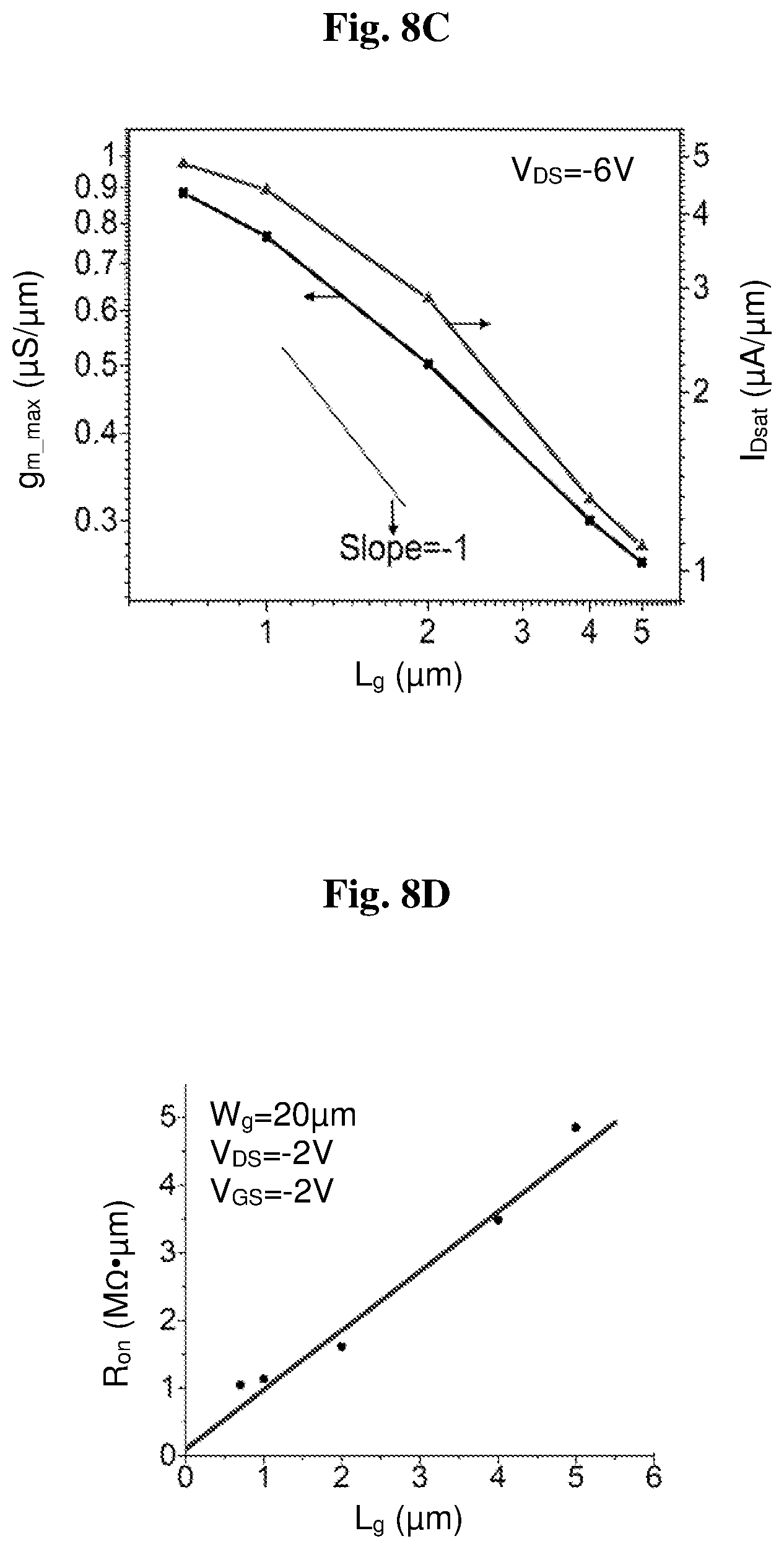
[0075] We have studied the impact of gate length, L.sub.g, on the electrical characteristics of 4.8 nm-thick WO.sub.3 devices. This is graphed in FIG. 8. FIG. 8A shows that the subthreshold behavior rapidly improves as L.sub.g increases. This probably stems from a combination of short-channel effects and reduced I.sub.g. In addition, we observe a significant improvement in peak transconductance, g.sub.mmax, as L.sub.g decreases (FIG. 8B). The threshold voltage, V.sub.T, shifts positive as gate length shortens. This could be explained by severe short-channel effects that arise from the use of a relatively thick gate dielectric coupled with the absence of body doping (del Alamo, 2017). FIG. 8C plots g.sub.mmax and the maximum drain current, I.sub.Dsat as a function of gate length at V.sub.DS=-6 V. The results indicate both g.sub.mmax and I.sub.Dsat correlate well with each other and scale in a well-behaved manner with L.sub.g.
[0076] In addition, we extracted the ON resistance of 4.8 nm-thick WO.sub.3 transistors with different L.sub.g at VGS=-2 V and V.sub.DS=-2 V (FIG. 8D). At this VGS, the ON resistance is largely saturated to its minimum value. From extrapolation of these data to L.sub.g=0, we estimated a total source/drain access resistance of 197 k.OMEGA..mu.m.
[0077] We have also studied the effect of temperature on the electrical characteristics of an L.sub.g=5 .mu.m, WO.sub.3=4.8 nm FET at 77 K. The results are presented in FIG. 9. At 77 K, we observe a large increase in I.sub.d and g.sub.m with g.sub.mmax scaling up by 3.5 times. We also see that I.sub.g was reduced by about two orders of magnitude (FIG. 9B). This results in significantly improved subthreshold behavior with the minimum subthreshold swing (S.sub.min) scaling down from 1225 mV/dec to 190 mV/dec and the ON-OFF ratio improving from .about.103 to .about.106, as the temperature is reduced from room temperature to 77K.
[0078] Device operation at 77 K was further studied by carrying out capacitance-voltage (C.sub.g--V.sub.GS) and I-V transfer (I.sub.d-V.sub.GS) characteristics in a device with 4.8 nm of WO.sub.3 and L.sub.g=5 .mu.m. The C-V characteristics were measured at 1 MHz with V.sub.DS=0 V. I.sub.d-V.sub.GS measurements were performed at VDs=-2 V. A typical C.sub.g-V.sub.GS result is shown in FIG. 10. From these data, we extract the gate voltage dependence of the sheet hole concentration (p.sub.s) and hole mobility (.mu..sub.p) (Radisavljevic et al., 2011; Balendhran et al., 2013). We also assume that the access resistance does not change with temperature since it is believed to be largely dominated by the contact resistance. We find that, in any case, the extracted mobility exhibits weak sensitivity to the actual value of access resistance that was used.
[0079] The inset of FIG. 10 graphs the sheet hole mobility (.mu.s) vs. sheet hole concentration (p.sub.s). Over most of its range, the mobility increases with hole concentration. This suggests that Coulomb scattering dominates at low temperature. We observe a maximum sheet hole concentration of about 3.1.times.10.sup.12 cm.sup.-2, The corresponding mobility, however, is 1.8 cm.sup.-2/Vsec. This is much lower than results obtained from Hall measurements at room temperature of similar unprocessed samples. This is also consistent with Coulomb scattering that could be due to gap states introduced as a result of WO.sub.3-x reduction during the device fabrication process (Greiner et al., 2012). The reduction in resistance that is observed as the temperature drops could be due to an insulator-to-metal transport transition recently reported by Mattoni et al. in WO.sub.3-x (Mattoni et al., 2017). This would also result in a reduced work function and degraded surface transfer doping efficiency at room temperature (Greiner et al., 2012).
[0080] The results of this Study reveal the potential of the D:H/WO.sub.3 system for future transistor applications but also illustrate the challenge of maintaining high TMO quality during device fabrication, an issue already noted in Vardi et al. (2014). To exploit the advantageous properties of the D:H/TMO system, transistor fabrication processes will need to be developed that maintain the integrity of the TMO layer.
REFERENCES
[0081] Balendhran, S., Deng, J., Ou, J. Z., Walia, S., Scott, J., Tang, J., Wang, K. L., Field, M. R., Russo, S., Zhuiykov, S., Strano, M. S., Medhekar, N., Sriram, S., Strano, M. S., Bhaskaran, M., Adv. Mater., 2013, 25(1), 109-114 [0082] Bertus, L. M., Faure, C., Danine, A., Labrugere, C., Campet, G., Rougier, A., Duta, A., Mater. Chem. Phys., 2013, 140, 49 [0083] Chakrapani, V., Angus, J. C., Anderson, A. B., Wolter, S. D., Stoner, B. R., Sumanasekera, G. U., Science, 2007, 318, 1424 [0084] Christiaens, P., Vermeeren, V., Wenmackers, S., Daenen, M., Haenen, K., Nesladek, M., vandeVen, M., Ameloot, M., Michiels, L., Wagner, P., Biosens. Bioelectron., 2006, 22, 170 [0085] Crawford, K. G., Cao, L., Qi, D. C., Tallaire, A., Limiti, E., Verona, C., Wee, A. T. S., Moran, D. A. J., Appl. Phys. Lett., 2016, 108(4), 042103 [0086] Dankerl, M., Lipert, A., Briner, S., Stutzel, E. U., Stutzmann, M., Garrido, J. A., Phys, Rev. Lett., 2011, 106, 16884 [0087] Daicho, A., Saito, T., Kurihara, S., Hiraiwa, A., Kawarada, H., J. Appl. Phys., 2014, 115, 223711 [0088] del Alamo, J. A., Integrated Microelectronic Devices: Physics and Modeling, 1st ed. London, U.K.: Pearson, 2017, sec. 10.2. [0089] Edmonds, M. T., Pakes, C. I., Mammadov, S., Zhang, W., Tadich, A., Ristein, J., Ley, L., Phys. Status Solidi A, 2011, 208(9), 2062 [0090] Geisler, M., Hugel, T., Adv. Mater., 2010, 22, 398 [0091] Gerling, L. G., Mahato, S., Voz, C., Alcubilla, R., Puigdollers, J., Appl. Sci., 2015, 5(4), 695 [0092] Greenwood, N. N., Earnshaw, A., Chemistry of the Elements (2nd ed). (Butterworth-Heinemann, 1997) [0093] Greiner, M. T., Chai, L., Helander, M. G., Tang, W. M., Lu, Z. H., Adv. Funct. Mater., 2012, 22(21), 4557-4568 [0094] Irfan, I., Turinske, A. J., Bao, Z. N., Gao, Y. L., Appl. Phys. Lett., 2012, 101(9), 093305 [0095] Imura, M., Banal, R. G., Liao, M., Liu, J., Aizawa, T., Tanaka, H. I. A., Mano, T., Koide, Y., J. Appl. Phys., 2017, 121, 025702 [0096] Kalish, R., J. Phys. D: Appl. Phys., 2007, 40, 6467 [0097] Kasu, M., Ueda, K., Ye, H., Yamauchi, Y., Sasaki, S., Makimoto, T., Electron. Lett., 2005, 41(22), 1248 [0098] Kasu, M., Ueda, K., Yamauchi, Y., Tallaire, A., Makimoto, T., Diamond Related Mater., 2007, 16(4-7), 1010 [0099] Kawarada, H., Appl. Phys. Lett., 2014, 105(1), 13510 [0100] Laikhtman, A., Lafosse, A., Le Coata, Y., Azriaa, R., Hoffman, A., Surface Science, 2004, 551, 99 [0101] Landstrass, M. I., Ravi, K. V., App. Phys. Lett., 1989, 55(14), 1391 [0102] Lassner, E., Schubert, W. D., Tungsten: Properties, Chemistry, Technology of the Element, Alloys, and Chemical Compounds. (Kluwer Academic, New York, 1999) [0103] Lud, S. Q., Steenackers, M., Jordan, R., Bruno, P., Gruen, D. M., Feulner, P., Garrido, J. A., Stutzmann, M., J. Am. Chem. Soc., 2006, 128, 16884 [0104] Maier, F., Riedel, M., Mantel, B., Ristein, J., Ley, L., Phys. Rev. Lett., 2000, 85(16), 3472 [0105] Maier, F., Ristein, J., Ley, L., Phys. Rev. B, 2001, 64, 165411 [0106] Mattoni, G., Filippetti, A., Manca, N., Zubko, P., Caviglia, A. D., Charge doping and large lattice expansion in oxygendeficient heteroepitaxial WO.sub.3, 2017, Available: https://arxiv.org/abs/1711.05106 [0107] Umezawa, H., Tsugawa, K., Yamanaka, S., Takeuchi, D., Okushi, H., Kawarada, H., Jpn. J Appl. Phys. Part 2, 1999, 38 (L1222) [0108] Suchitra, Pan, J., Waghmare, U. V., J Appl. Phys., 2014, 116(3), 034304 [0109] Poh, W. C., Loh, K. P., De Zhang, W., Triparthy, S., Langmuir, 2004, 20(13), 5484 [0110] Qi, D., Chen, W., Gao, X., Wang, L., Chen, S., Loh, K. P., Wee, A. T. S., J. Am. Chem. Soc., 2007, 129, 8084 [0111] Radisavljevic, B., Radenovic, A., Brivio, J., Giacometti, V., Kis, A., Nature Nanotechnol., 2011, 6(3), 147-150 [0112] Russell, S. A. O., Cao, L., Qi, D., Tallaire, A., Crawford, K. G., Wee, A. T. S., Moran, D. A. J., Appl. Phys. Lett., 2013, 103, 202112 [0113] Sato, H., Kasu, M., ibid, 2013, 31, 47 [0114] Sauerer, C., Ertl, F., Nebel, C. E., Stutzmann, M., Bergonzo, P., Williams, O. A., Jackman, R. A., Phys. Status Solidi A, 2001, 186(2), 241 [0115] Strobel, P., Riedel, M., Ristein, J., Ley, L., Nature, 2004, 430, 439 [0116] Strobel, P., Ristein, J., Ley, L., Seppelt, K., Goldt, I. V., Boltalina, O., Diamond Relat. Mater., 2006, 15, 720 [0117] Sussmann, R. S., CVD diamond for Electronic Devices. (John Wiley & Sons, Chichester, 2009). [0118] Taniuchi, H., Umezawa, H., Arima, T., Tachiki, M., Kawarada, H., Electron Device Lett., 2001, 22(8), 390 [0119] Tordjman, M., Saguy, C., Bolker, A., Kalish, R., Adv. Mater. Interfaces, 2014, 1, 1300155 [0120] Vardi, A., Tordjman, M., del Alamo, J. A., Kalish, R., IEEE Electron Device Lett., 2014, 35(12), 1320-1322 [0121] Verona, C., Ciccognani, W., Colangeli, S., Limiti, E., Marinelli, M., Verona-Rinati, G., J. Appl. Phys., 2016, 120(2), 025104 [0122] Wade, T., Geis, M. W., Fedynyshyna, T. H., Vitalea, S. A., Varghesea, J. O., Lennona, D. M., Nemanichc, R. J., Grotjohnb, T. A., Hollis, M. A., Diam. Rel. Mat., 2017, 76, 79 [0123] Yang, W., Auciello, O., Butler, J. E., Cai, W., Carlisle, J. A., Gerbi, J. E., Gruen, D. M., Knickerbocker, T., Lasseter, T. L., Russell, J. N., Smith, Jr. L. M., Hamers, R. J., Nat. Mater., 2002, 1, 253 [0124] Di Yao, D., Ou, J. Z., Latham, K., Zhuiykov, S., O'Mullane, A. P., Kalantar-zadeh, K., Cryst. Growth & Des., 2012, 12(4), 1865 [0125] Yom-Tov, N., Saguy, C., Bolker, A., Kalish, R., Yaish, Y. E., J. Appl. Phys., 2010, 108, 043711 [0126] Yoo, S. J., Chang, J. H., Lee, J. H., Moon, C. K., Wu, C. I., Kim, J. J., Sci. Rep., 2014, 4, 3902
* * * * *
References
D00000
D00001
D00002
D00003
D00004
D00005
D00006
D00007
D00008
D00009
D00010
D00011
D00012

D00013

XML
uspto.report is an independent third-party trademark research tool that is not affiliated, endorsed, or sponsored by the United States Patent and Trademark Office (USPTO) or any other governmental organization. The information provided by uspto.report is based on publicly available data at the time of writing and is intended for informational purposes only.
While we strive to provide accurate and up-to-date information, we do not guarantee the accuracy, completeness, reliability, or suitability of the information displayed on this site. The use of this site is at your own risk. Any reliance you place on such information is therefore strictly at your own risk.
All official trademark data, including owner information, should be verified by visiting the official USPTO website at www.uspto.gov. This site is not intended to replace professional legal advice and should not be used as a substitute for consulting with a legal professional who is knowledgeable about trademark law.