Three Dimensional Antenna Array Module
Yoon; Seunghwan ; et al.
U.S. patent application number 17/004373 was filed with the patent office on 2020-12-17 for three dimensional antenna array module. The applicant listed for this patent is Movandi Corporation. Invention is credited to Alfred Grau Besoli, Michael Boers, Franco De Flaviis, Sam Gharavi, Ahmadreza Rofougaran, Maryam Rofougaran, Donghyup Shin, Farid Shirinfar, Kartik Sridharan, Stephen Wu, Seunghwan Yoon.
| Application Number | 20200395682 17/004373 |
| Document ID | / |
| Family ID | 1000005051740 |
| Filed Date | 2020-12-17 |


| United States Patent Application | 20200395682 |
| Kind Code | A1 |
| Yoon; Seunghwan ; et al. | December 17, 2020 |
THREE DIMENSIONAL ANTENNA ARRAY MODULE
Abstract
Provided is an apparatus including a plurality of antenna modules and a printed circuit board (PCB) having a plurality of holes embedded with a heat sink. Each antenna module includes an antenna substrate, a plurality of three-dimensional (3-D) antenna cells mounted on a first surface of the antenna substrate, and a plurality of packaged circuitry mounted on a second surface of the antenna substrate. The plurality of packaged circuitry are electrically connected with the plurality of 3-D antenna cells. Each antenna module is mounted on the plurality of holes via a corresponding packaged circuitry of the plurality of packaged circuitry.
| Inventors: | Yoon; Seunghwan; (Irvine, CA) ; De Flaviis; Franco; (Irvine, CA) ; Besoli; Alfred Grau; (Irvine, CA) ; Sridharan; Kartik; (San Diego, CA) ; Rofougaran; Ahmadreza; (Newport Beach, CA) ; Boers; Michael; (South Turramurra, AU) ; Gharavi; Sam; (Irvine, CA) ; Shin; Donghyup; (Irvine, CA) ; Shirinfar; Farid; (Granada Hills, CA) ; Wu; Stephen; (Fountain Valley, CA) ; Rofougaran; Maryam; (Rancho Palos Verdes, CA) | ||||||||||
| Applicant: |
|
||||||||||
|---|---|---|---|---|---|---|---|---|---|---|---|
| Family ID: | 1000005051740 | ||||||||||
| Appl. No.: | 17/004373 | ||||||||||
| Filed: | August 27, 2020 |
Related U.S. Patent Documents
| Application Number | Filing Date | Patent Number | ||
|---|---|---|---|---|
| 15607750 | May 30, 2017 | |||
| 17004373 | ||||
| Current U.S. Class: | 1/1 |
| Current CPC Class: | H01Q 1/2283 20130101; H01Q 9/045 20130101; H01Q 21/0025 20130101; H01Q 21/065 20130101 |
| International Class: | H01Q 21/06 20060101 H01Q021/06; H01Q 21/00 20060101 H01Q021/00; H01Q 1/22 20060101 H01Q001/22; H01Q 9/04 20060101 H01Q009/04 |
Claims
1. An apparatus, comprising: a plurality of antenna modules; and a printed circuit board (PCB) having a plurality of holes embedded with a heat sink, wherein each antenna module of the plurality of antenna modules comprises: an antenna substrate; a plurality of three-dimensional (3-D) antenna cells mounted on a first surface of the antenna substrate; and a plurality of packaged circuitry mounted on a second surface of the antenna substrate, wherein the plurality of packaged circuitry are electrically connected with the plurality of 3-D antenna cells, wherein each antenna module of the plurality of antenna modules is mounted on the plurality of holes via a corresponding packaged circuitry of the plurality of packaged circuitry.
2. The apparatus according to claim 1, wherein each of the plurality of 3-D antenna cells is a 3-D metal stamped antenna.
3. The apparatus according to claim 1, wherein a height of each of the plurality of 3-D antenna cells is one-fourth of wavelength at an operational frequency.
4. The apparatus according to claim 1, wherein a width of each of the plurality of 3-D antenna cells is half of wavelength at an operational frequency.
5. The apparatus according to claim 1, wherein each of the plurality of 3-D antenna cells comprises a raised antenna patch with air dielectric.
6. The apparatus according to claim 5, wherein the raised antenna patch comprises a top plate over a ground plane in each of the plurality of 3-D antenna cells.
7. The apparatus according to claim 5, wherein the raised antenna patch comprises four projections having outwardly increasing widths.
8. The apparatus according to claim 5, wherein the raised antenna patch comprises a top plate at a height greater than a ground plane in each of the plurality of 3-D antenna cells.
9. The apparatus according to claim 1, wherein each of the plurality of 3-D antenna cells further comprises four supporting legs.
10. The apparatus according to claim 9, wherein each of the four supporting legs is located between a pair of adjacent projections of four projections associated with a raised antenna patch of each of the plurality of 3-D antenna cells.
11. The apparatus according to claim 1, wherein the plurality of packaged circuitry comprises a plurality of radio-frequency (RF) chips and at least one mixer chip that are mounted on a second surface of the antenna substrate.
12. The apparatus according to claim 11, wherein the plurality of packaged circuitry is further mounted on a printed circuit board (PCB) based on the plurality of holes in the PCB.
13. The apparatus according to claim 1, further comprises a first supporting ball on a first side of a packaged circuitry of the plurality of packaged circuitry and a second supporting ball on a second side of the packaged circuitry on the second surface of the antenna substrate.
14. The apparatus according to claim 1, wherein the heat sink is in direct contact with the PCB and the plurality of holes.
Description
CROSS-REFERENCE TO RELATED APPLICATIONS/INCORPORATION BY REFERENCE
[0001] This Patent Application makes reference to, claims priority to, claims the benefit of, and is a Divisional Application of U.S. patent application Ser. No. 15/607,750, filed May 30, 2017.
[0002] This Application also makes reference to U.S. Pat. No. 10,062,965, which was filed on Apr. 14, 2017.
[0003] The above referenced Application is hereby incorporated herein by reference in its entirety.
FIELD OF TECHNOLOGY
[0004] Certain embodiments of the disclosure relate to an antenna module. More specifically, certain embodiments of the disclosure relate to a three-dimensional (3-D) antenna cells for antenna modules.
BACKGROUND
[0005] Current decade is witnessing a rapid growth and evolvement in the field of wireless communication. For instance, in 5G wireless communication, advanced antennas and radar systems (such as phased antenna array modules) are utilized for beam forming by phase shifting and amplitude control techniques, without a physical change in direction or orientation and further, without a need for mechanical parts to effect such changes in direction or orientation.
[0006] Typically, a phased antenna array module includes a substrate and a radio frequency (RF) antenna cell provided in relation to the substrate. To design a radio frequency frontend (RFFE), for every phased antenna array module, a designer may also be required to purchase and integrate various semiconductor chips in order to realize their design objectives. The designer may also be required to consider other factors, such as the design of the antenna, various connections, transitions from the antenna cell to the semiconductor chips and the like, which may me quite complex, tedious, and time consuming. Further, impaired antenna impedance matching during scanning or beam forming results in increased return loss (defined as ratio of power returned from an antenna to power delivered to the antenna). Also, the choice of substrate materials is important is thicker substrates are more expensive and may behave as waveguides, adversely affecting radiation of RF waves from the antennas, and resulting in increased loss and lower efficiency. Thus, there is a need for a highly efficient antenna array module with a flexible design for RFFE (in the wireless communication systems) that overcomes the deficiencies in the art.
[0007] Further limitations and disadvantages of conventional and traditional approaches will become apparent to one of skill in the art, through comparison of such systems with some aspects of the present disclosure as set forth in the remainder of the present application with reference to the drawings.
BRIEF SUMMARY OF THE DISCLOSURE
[0008] Three-dimensional (3-D) antenna array module for use in RF communication system, substantially as shown in and/or described in connection with at least one of the figures, as set forth more completely in the claims.
[0009] These and other advantages, aspects and novel features of the present disclosure, as well as details of an illustrated embodiment thereof, will be more fully understood from the following description and drawings.
BRIEF DESCRIPTION OF DRAWINGS
[0010] FIG. 1 is an exemplary arrangement of 3-D antenna array modules on a printed circuit board (PCB), in accordance with an exemplary embodiment of the disclosure.
[0011] FIG. 2 illustrates a perspective view of an antenna cell of a 3-D antenna array module, in accordance with an exemplary embodiment of the disclosure.
[0012] FIG. 3A illustrates a perspective view of an exemplary 3-D antenna array module, in accordance with an exemplary embodiment of the disclosure.
[0013] FIG. 3B illustrates a top view of an exemplary 3-D antenna array module, in accordance with an exemplary embodiment of the disclosure.
[0014] FIG. 3C illustrates a rear view of an exemplary 3-D antenna array module, in accordance with an exemplary embodiment of the disclosure.
[0015] FIG. 4 illustrates a side view arrangement of antenna cells of a 3-D antenna array module on a PCB, in accordance with an exemplary embodiment of the disclosure.
DETAILED DESCRIPTION OF THE DISCLOSURE
[0016] Certain embodiments of the disclosure may be found in a 3-D antenna array module for use in RF communication system. In the following description, reference is made to the accompanying drawings, which form a part hereof, and in which is shown, by way of illustration, various embodiments of the present disclosure.
[0017] FIG. 1 is an exemplary arrangement of 3-D antenna array modules on a PCB, in accordance with an exemplary embodiment of the disclosure. With reference to FIG. 1, there is shown an exemplary arrangement diagram 100. The exemplary arrangement diagram 100 corresponds to integration of a plurality of antenna modules 106 (for example, a first antenna module 106a, a second antenna module 106b, and a third antenna module 106c) on a PCB 102. The PCB 102 may have a top PCB surface 102a and a bottom PCB surface 102b. There is further shown a plurality of holes 108, for example, a first gap or hole 108a, a second gap or hole 108b, and a third gap 108c that are included in the PCB 102. There is further shown a heat sink 104 in direct contact with the bottom PCB surface 102b and further embedded within the plurality of holes 108. With reference to the plurality of antenna modules 106, for example, the first antenna module 106a, there is shown an antenna substrate 110, a plurality of 3-D antenna cells 112 (for example, a first antenna cell 112a, a second antenna cell 112b, a third antenna cell 112c, and a fourth antenna cell 112d), a plurality of packaged circuitry 114, and a plurality of supporting balls 116.
[0018] In accordance with an embodiment, the heat sink 104 may be in direct contact with the bottom PCB surface 102b of the PCB 102, as shown in FIG. 1. Further, the plurality of holes 108 included in the PCB 102 may be embedded with the heat sink 104. The heat sink 104 embedded within the plurality of holes 108 of the PCB 102 may dissipate heat generated by, for example, the plurality of 3-D antenna cells 112, the plurality of packaged circuitry 114, one or more power amplifiers (not shown), and other heat generating circuitry or components associated with the plurality of antenna modules 106 and the PCB 102. With such arrangement, the top PCB surface 102a of the PCB 102 and the plurality of portions of the heat sink 104 embedded within the plurality of holes 108 forms a mounting surface of the PCB 102 on which the plurality of antenna modules 106 may be mounted.
[0019] The plurality of antenna modules 106, for example, the first antenna module 106a, may be obtained based on integration of the plurality of 3-D antenna cells 112, the plurality of packaged circuitry 114, and the plurality of supporting balls 116 on the antenna substrate 110. The antenna substrate 110 may be composed of a low loss substrate material. The low loss substrate material may exhibit characteristics, such as low loss tangent, high adhesion strength, high insulation reliability, low roughness, and/or the like.
[0020] In accordance with an exemplary embodiment, the plurality of 3-D antenna cells 112 may be integrated on a first surface of the antenna substrate 110. In accordance with an embodiment, each of the plurality of 3-D antenna cells 112 may correspond to a plurality of small packages mounted on an antenna module, for example, the first antenna module 106a. In accordance with another embodiment, each of the plurality of 3-D antenna cells 112 may correspond to a 3-D metal stamped antenna, which provide high efficiency at a relatively low cost. A structure of a 3-D antenna cell has been described in detail in FIG. 2.
[0021] Further, the plurality of packaged circuitry 114 may be integrated on a second surface of the antenna substrate 110, as shown. Each of the plurality of packaged circuitry 114 in the first antenna module 106a may comprise suitable logic, circuitry, interfaces, and/or code that may be configured to execute a set of instructions stored in a memory (not shown) to execute one or more (real-time or non-real-time) operations. The plurality of packaged circuitry 114 may further comprise a plurality of RF chips and at least one mixer chip. The plurality of RF chips and the at least one mixer chip in the plurality of packaged circuitry 114 may be integrated on the second surface of the antenna substrate 110. Further, the plurality of packaged circuitry 114 may be connected through an electromagnetic transmission line with the plurality of 3-D antenna cells 112.
[0022] Further, the plurality of supporting balls 116 may be integrated on the second surface of the antenna substrate 110, as shown. The plurality of supporting balls 116 may be integrated to provide uniform spacing between the first antenna module 106a and the PCB 102. Furthermore, the plurality of supporting balls 116 may be integrated to provide uniform support to the first antenna module 106a on the PCB 102. Each of the plurality of supporting balls 116 may be composed of materials, such as, but not limited to, an insulating material, a non-insulating material, a conductive material, a non-conductive material, or a combination thereof.
[0023] Based on at least the above integration of the plurality of 3-D antenna cells 112, the plurality of packaged circuitry 114, and the plurality of supporting balls 116 on the antenna substrate 110, the first antenna module 106a may be obtained. Similar to the first antenna module 106a, the second antenna module 106b and the third antenna module 106c may be obtained, without deviation from the scope of the disclosure.
[0024] Further, in accordance with an embodiment, each of the plurality of antenna modules 106 may be mounted on the plurality of portions of the heat sink 104 embedded within the plurality of holes 108 that forms the mounting surface of the PCB 102. The plurality of antenna modules 106 may be mounted on the plurality of portions in such a manner that the corresponding packaged circuitry is in direct contact with portions of the heat sink 104 embedded within the plurality of holes 108 to realize a 3-D antenna panel. In an exemplary implementation, the 3-D antenna panel comprising 3-D antenna cells, for example, the plurality of antenna cells 112, may be used in conjunction with 5G wireless communications (5th generation mobile networks or 5th generation wireless systems). In another exemplary implementation, the 3-D antenna panel comprising the 3-D antenna cells may be used in conjunction with commercial radar systems and geostationary communication satellites or low earth orbit satellites.
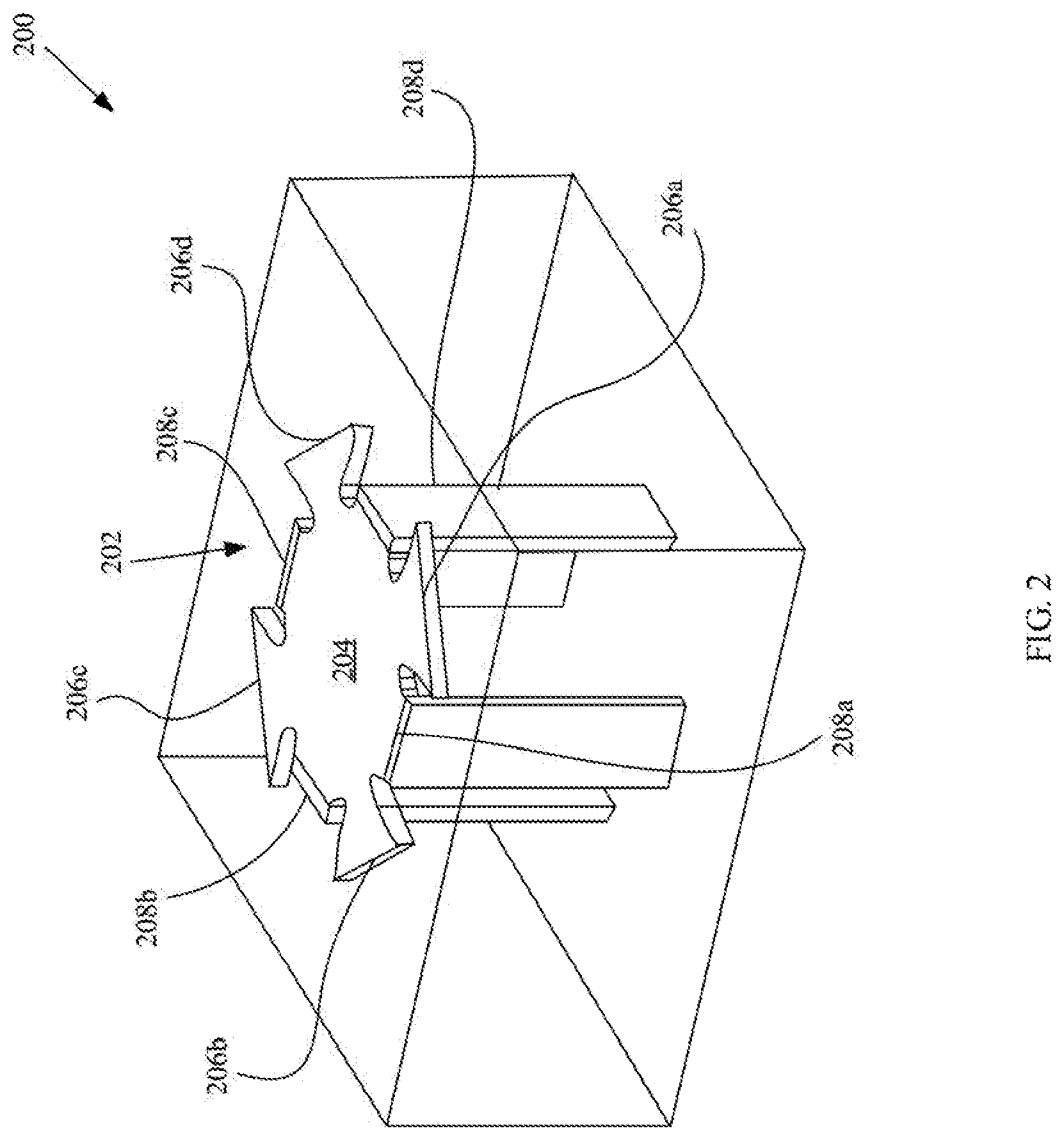
[0025] FIG. 2 illustrates a perspective view of an exemplary antenna cell of a 3-D antenna array module, in accordance with an exemplary embodiment of the disclosure. With reference to FIG. 2, there is shown a 3-D antenna cell 200 as one of the antenna cells associated with each of the plurality of antenna modules 106. For example, the 3-D antenna cell 200 may correspond to one of the plurality of antenna cells 112, such as the first antenna cell 112a, the second antenna cell 112b, the third antenna cell 112c, or the fourth antenna cell 112d of the first antenna module 106a. With reference to the 3-D antenna cell 200, there is shown a raised antenna patch 202, having a top plate 204 with projections 206a, 206b, 206c, and 206d, and supporting legs 208a, 208b, 208c, and 208d.
[0026] In accordance with an embodiment, the 3-D antenna cell 200 may correspond to a 3-D metal stamped antenna for use in a wireless communication network, such as 5G wireless communications. The wireless communication network may facilitate extremely high frequency (EHF), which is the band of radio frequencies in the electromagnetic spectrum from 30 to 300 gigahertz. Such radio frequencies have wavelengths from ten to one millimeter, referred to as millimeterwave (mmWave). In such a scenario, a height of the 3-D antenna cell 200 may correspond to one-fourth of the mmWave. Further, a width of the 3-D antenna cell 200 may correspond to half of the mmWave. Further, a distance between two antenna cells may correspond to half of the mmWave.
[0027] Further, the four projections 206a, 206b, 206c, and 206d of the raised antenna patch 202 may be situated between a pair of adjacent supporting legs of the four supporting legs 208a, 208b, 208c, and 208d. The four projections 206a, 206b, 206c, and 206d may have outwardly increasing widths i.e., a width an inner portion of each of the four projections 206a, 206b, 206c, and 206d is less than a width of an outer portion of each of the four projections 206a, 206b, 206c, and 206d. Further, the width of each of the four projections 206a, 206b, 206c, and 206d gradually increases while moving outward from the inner portion towards the outer portion.
[0028] Further, the four supporting legs 208a, 208b, 208c, and 208d of the raised antenna patch 202 may be situated between a pair of adjacent projections of the four projections 206a, 206b, 206c, and 206d. For example, supporting leg 208a is situated between the adjacent projections 206a and 206b. The four supporting legs 208a, 208b, 208c, and 208d extend from top plate 204 of the raised antenna patch 202. Based on the usage of the four supporting legs 208a, 208b, 208c, and 208d in the 3-D antenna cell, the four supporting legs 208a, 208b, 208c, and 208d may carry RF signals between the top plate 204 of the raised antenna patch 202 and components (for example, the plurality of packaged circuitry 114) at second surface of the antenna substrate 110. The material of the raised antenna patch 202 may be copper, stainless steel, or any other conductive material. The raised antenna patch 202 may be formed by bending a substantially flat copper patch at the four supporting legs 208a, 208b, 208c, and 208d. The flat patch may have relief cuts between the four projections 206a, 206b, 206c, and 206d and the four supporting legs 208a, 208b, 208c, and 208d in order to facilitate bending supporting legs 208a, 208b, 208c, and 208d without bending top plate 204.
[0029] In accordance with an embodiment, the use of the 3-D antenna cell 200 in the 3-D antenna panel may result in improved matching conditions, scan range, and bandwidth. The improved matching conditions, scan range, and bandwidth are attributed to factors, such as the shape of the raised antenna patch 202 (for example, the projections 206a, 206b, 206c, and 206d), the use of air as dielectric to obtain the desired height of the raised antenna patch 202 at low cost, and shielding fence around the 3-D antenna cell 200.
[0030] In accordance with an embodiment, the raised antenna patch 202 uses air as a dielectric, instead of using solid material (such as FR4) as a dielectric, and thus may present several advantages. For example, air, unlike typical solid dielectrics, does not excite RF waves within the dielectric or on the surface thereof, and thus decreases power loss and increases efficiency. Moreover, since top plate 204 may have an increased height, the bandwidth of the raised antenna patch 202 with air dielectric may be significantly improved without increasing manufacturing cost. Furthermore, the use of air as the dielectric is free of cost, and may not result in formation of a waveguide since RF waves would not be trapped when air is used as the dielectric. In addition, the raised antenna patch 202 having the projections 206a, 206b, 206c, and 206d may provide improved matching with transmission lines, thereby, delivering power to the antenna over a wide range of scan angles, resulting in lower return loss.
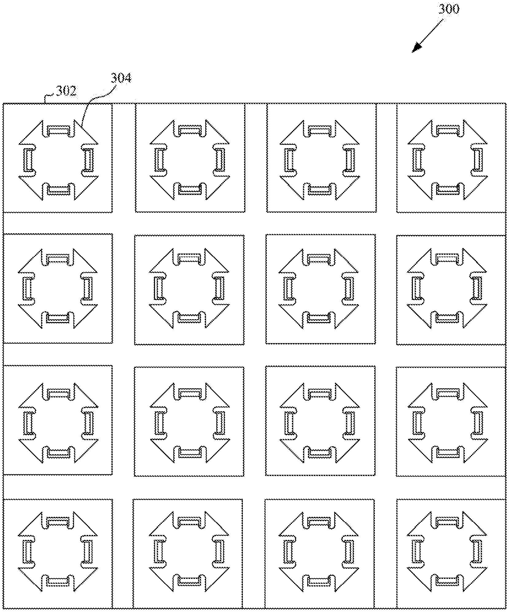
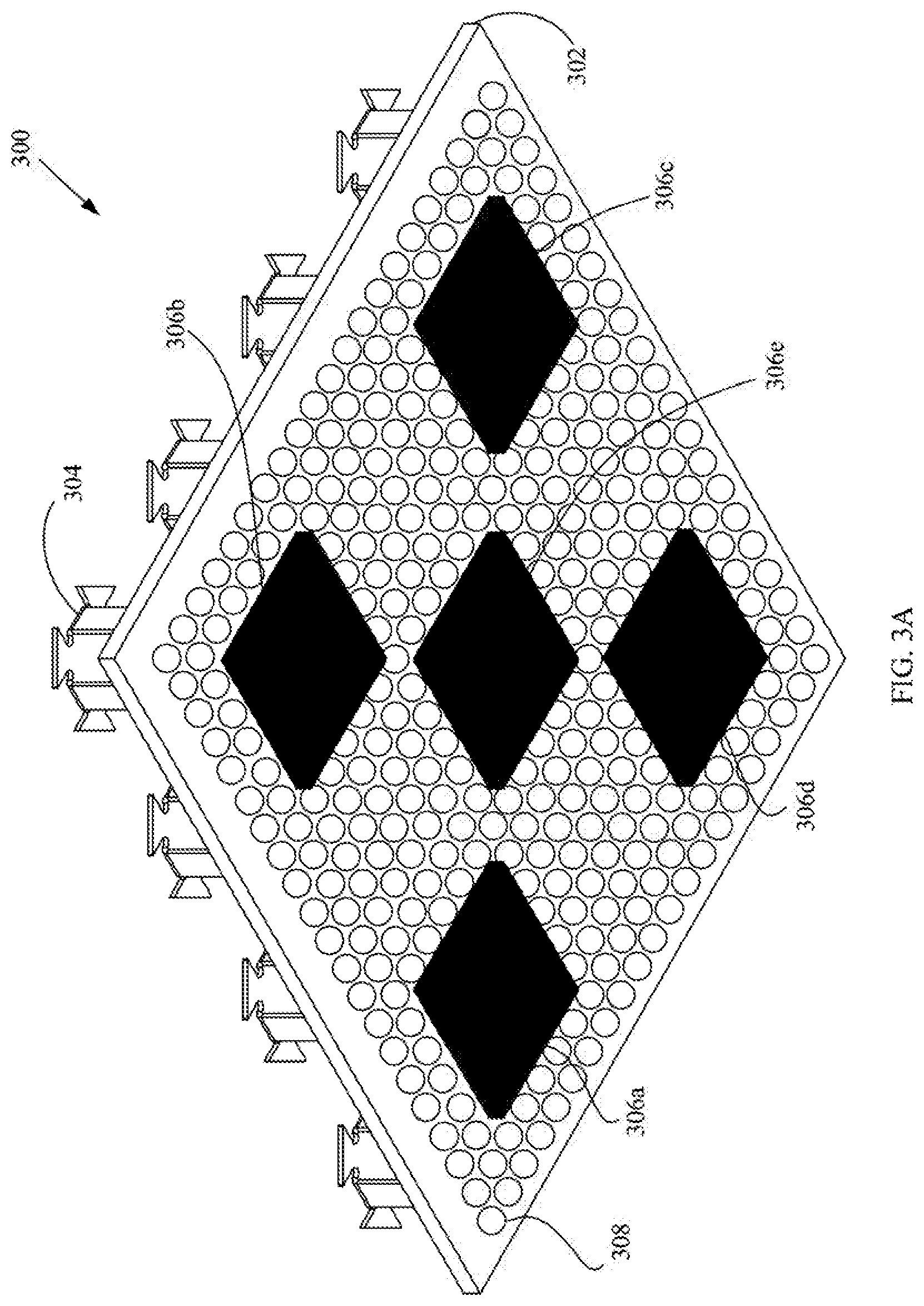
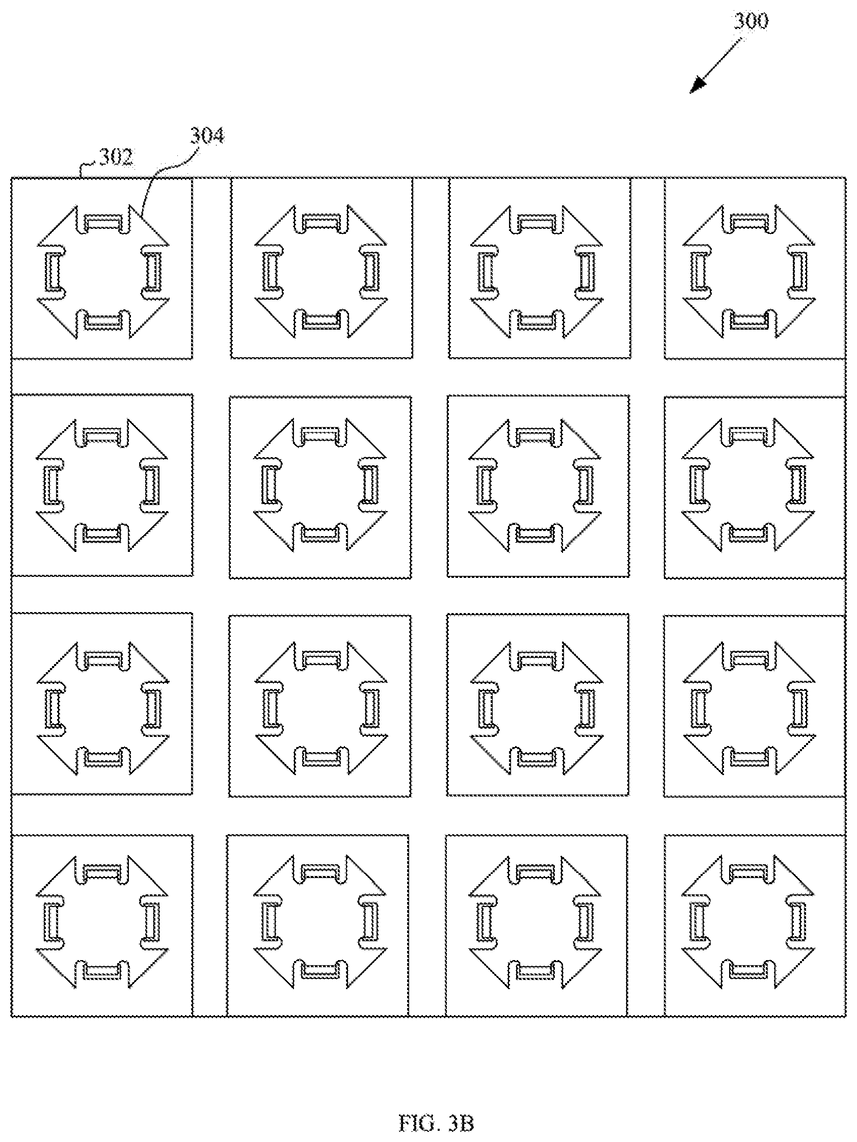
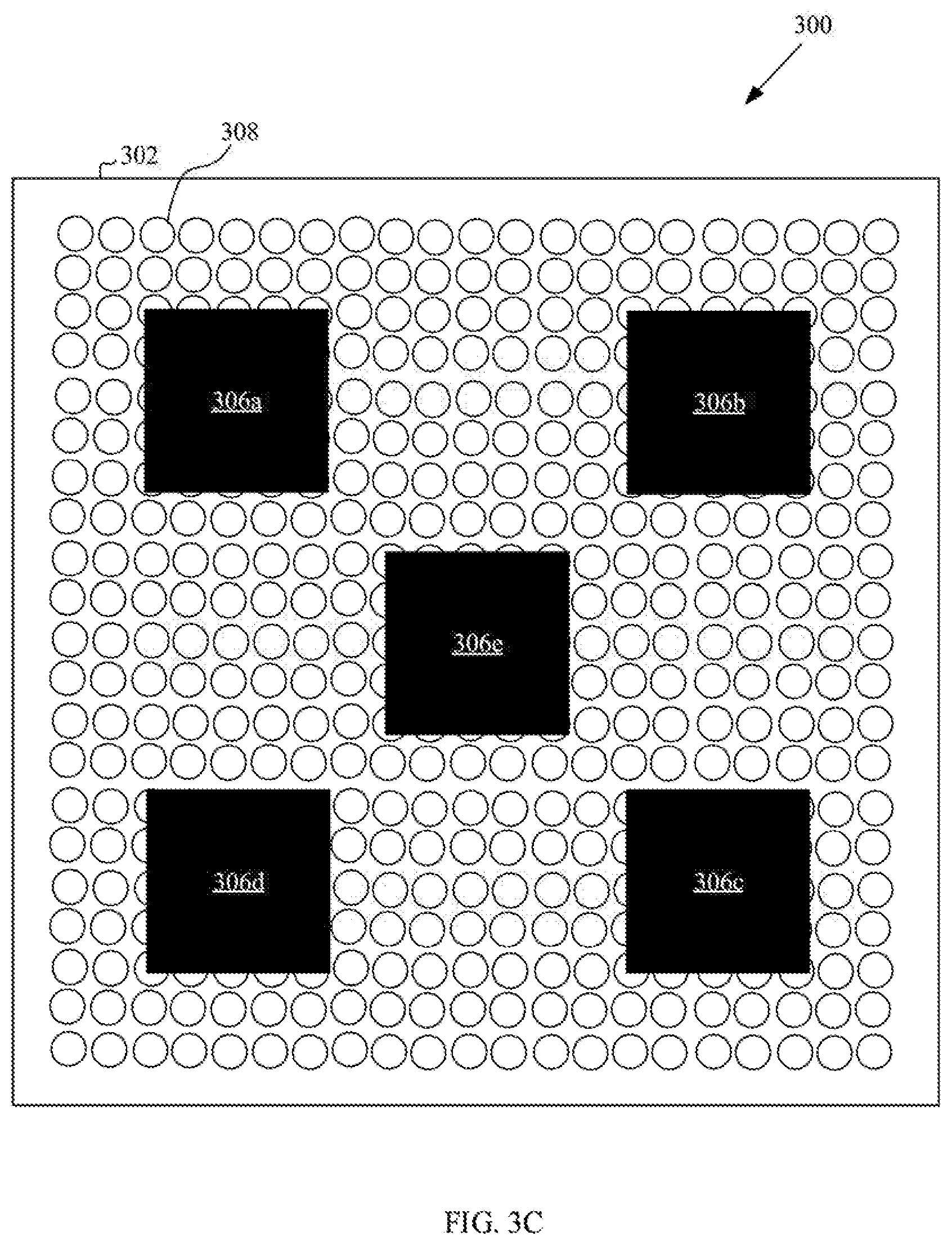
[0031] FIG. 3A illustrates a perspective view of an exemplary 3-D antenna array module, in accordance with an exemplary embodiment of the disclosure. With reference to FIG. 3A, there is shown an antenna module 300. The antenna module 300 may correspond to one of the plurality of antenna modules 106, such as the first antenna module 106a, as shown in FIG. 1. With reference to the antenna module 300, there is further shown an antenna substrate 302 that may generally correspond to the antenna substrate 110 of the first antenna module 106a, as shown in FIG. 1. There is further shown a plurality of 3-D antenna cells 304 that may generally correspond to the plurality of antenna cells 112 of the first antenna module 106a, as shown in FIG. 1. There is further shown a plurality of packaged circuitry, such as a first RF chip 306a, a second RF chip 306b, a third RF chip 306c, a fourth RF chip 306d, and a mixer chip 306e, that may generally correspond to the plurality of packaged circuitry 114 of the first antenna module 106a, as shown in FIG. 1. There is further shown a plurality of supporting balls 308 that may generally correspond to the plurality of supporting balls 116 of the first antenna module 106a, as shown in FIG. 1.
[0032] As shown in FIG. 3A, the plurality of 3-D antenna cells 304 may be mounted on an upper surface of the antenna substrate 302. A specified count of 3-D antenna cells from the plurality of 3-D antenna cells 304 may be connected with each of the first RF chip 306a, the second RF chip 306b, the third RF chip 306c, or the fourth RF chip 306d. Further, the plurality of 3-D antenna cells 304 may be connected with the mixer chip 306e. In another exemplary embodiment, at least one of the first RF chip 306a, the second RF chip 306b, the third RF chip 306c, or the fourth RF chip 306d may be connected with the mixer chip 306e. The first RF chip 306a, the second RF chip 306b, the third RF chip 306c, the fourth RF chip 306d, and the mixer chip 306e may be mounted on a lower surface of the antenna substrate 302, as shown. The lower surface of the antenna substrate 302 may further include the plurality of supporting balls 308 that are designed to maintain uniform space and support to the antenna module when the antenna module 300 is mounted on the PCB 102.
[0033] FIG. 3B illustrates a top view of the antenna module 300, in accordance with an exemplary embodiment of the disclosure. The antenna module 300 may correspond to a "4.times.4" array of the plurality of 3-D antenna cells 304. Each of the "4.times.4" array of the plurality of 3-D antenna cells 304 is mounted on the top surface of the antenna substrate.
[0034] FIG. 3C illustrates a rear view of the antenna module 300, in accordance with an exemplary embodiment of the disclosure. The first RF chip 306a, the second RF chip 306b, the third RF chip 306c, the fourth RF chip 306d, and the mixer chip 306e are mounted on the lower surface of the antenna substrate 302. Further, each of the "4.times.4" array of the plurality of 3-D antenna cells 304 is electrically connected with at least one of the first RF chip 306a, the second RF chip 306b, the third RF chip 306c, the fourth RF chip 306d, or the mixer chip 306e.
[0035] FIGS. 3A, 3B, and 3C show a 3-D antenna panel with one antenna module 300 having "4.times.4" array of the plurality of 3-D antenna cells 304 that include "16" 3-D antenna cells. However, a count of the 3-D antenna cells is for exemplary purposes and should not be construed to limit the scope of the disclosure. In practice, for example, when the 3-D antenna panel is used in conjunction with 5G wireless communications, the 3-D antenna panel may include "144" 3-D antennas cells. Therefore, "9" antenna modules of "4.times.4" array of the plurality of 3-D antenna cells 304 may be required. Furthermore, when the 3-D antenna panel is used in conjunction with commercial geostationary communication satellites or low earth orbit satellites, the 3-D antenna panel may be even larger, and have, for example, "400" 3-D antennas cells. Therefore, "25" antenna modules of "4.times.4" array of the plurality of 3-D antenna cells 304 may be required. In other examples, the 3-D antenna panel may have any other number of 3-D antenna cells. In general, the performance of the 3-D antenna panel improves with the number of 3-D antenna cells.
[0036] FIG. 4 illustrates a side view arrangement of antenna cells of a 3-D antenna module on a PCB, in accordance with an exemplary embodiment of the disclosure. With reference to FIG. 4, there is shown a side view arrangement 400 that is described in conjunction with FIGS. 1, 2, and 3A to 3C. The side view arrangement 400 corresponds to side view integration of the plurality of 3-D antenna cells 112 on a first surface (i.e., a top surface) of the antenna substrate 110 of the first antenna module 106a. The plurality of 3-D antenna cells 112 may be electrically (or magnetically) connected with the plurality of packaged circuitry 114 (i.e., the RF and mixer chips 306). The RF and mixer chips 306 may be integrated with a second surface (i.e., a bottom surface) of the antenna substrate 110. Further, the first antenna module 106a is integrated on the PCB 102 via the plurality of packaged circuitry 114 and the plurality of supporting balls 116. The plurality of 3-D antenna cells 112 may result in improved bandwidth. Further, the use of the plurality of 3-D antenna cells 112, as shown in FIG. 4, may provide improved matching with transmission lines, thereby, delivering power to the first antenna module 106a over a wide range of scan angles, resulting in lower return loss. The 3-D antenna module may facilitate the integration of the chips and the antenna cells as single package implementation. The 3-D antenna modules simplify the design of 5G RFFE and enhance the flexibility to extend. The antenna impedance matching is improved resulting in reduced return loss. In PCB 102, as the signals are low frequency, therefore generic substrates (such as organic based material) may be utilized instead of expensive substrate, thereby saving the overall cost for realization. The 3-D antenna modules may further attract the users to design customized front end system.
[0037] Thus, various implementations of the present application achieve improved large scale integration of 3-D antenna panels for use in 5G applications. From the above description it is manifest that various techniques can be used for implementing the concepts described in the present application without departing from the scope of those concepts. Moreover, while the concepts have been described with specific reference to certain implementations, a person of ordinary skill in the art would recognize that changes can be made in form and detail without departing from the scope of those concepts. As such, the described implementations are to be considered in all respects as illustrative and not restrictive. It should also be understood that the present application is not limited to the particular implementations described above, but many rearrangements, modifications, and substitutions are possible without departing from the scope of the present disclosure.
* * * * *
D00000
D00001
D00002
D00003
D00004
D00005
D00006
XML
uspto.report is an independent third-party trademark research tool that is not affiliated, endorsed, or sponsored by the United States Patent and Trademark Office (USPTO) or any other governmental organization. The information provided by uspto.report is based on publicly available data at the time of writing and is intended for informational purposes only.
While we strive to provide accurate and up-to-date information, we do not guarantee the accuracy, completeness, reliability, or suitability of the information displayed on this site. The use of this site is at your own risk. Any reliance you place on such information is therefore strictly at your own risk.
All official trademark data, including owner information, should be verified by visiting the official USPTO website at www.uspto.gov. This site is not intended to replace professional legal advice and should not be used as a substitute for consulting with a legal professional who is knowledgeable about trademark law.