Method For Depositing A Phosphorus Doped Silicon Arsenide Film And Related Semiconductor Device Structures
Lo; Chi-Wei ; et al.
U.S. patent application number 17/009093 was filed with the patent office on 2020-12-17 for method for depositing a phosphorus doped silicon arsenide film and related semiconductor device structures. The applicant listed for this patent is ASM IP Holding B.V.. Invention is credited to Alexandros Demos, Raj Kumar, Chi-Wei Lo.
| Application Number | 20200395444 17/009093 |
| Document ID | / |
| Family ID | 1000005063055 |
| Filed Date | 2020-12-17 |


| United States Patent Application | 20200395444 |
| Kind Code | A1 |
| Lo; Chi-Wei ; et al. | December 17, 2020 |
METHOD FOR DEPOSITING A PHOSPHORUS DOPED SILICON ARSENIDE FILM AND RELATED SEMICONDUCTOR DEVICE STRUCTURES
Abstract
A method for depositing a phosphorus doped silicon arsenide film is disclosed. The method may include, providing a substrate within a reaction chamber, heating the substrate to a deposition temperature, exposing the substrate to a silicon precursor, an arsenic precursor, and a phosphorus dopant precursor, and depositing the phosphorus doped silicon arsenide film over a surface of the substrate. Semiconductor device structures including a phosphorus doped silicon arsenide film deposited by the methods of the disclosure are also provided.
| Inventors: | Lo; Chi-Wei; (Phoenix, AZ) ; Demos; Alexandros; (Scottsdale, AZ) ; Kumar; Raj; (Chandler, AZ) | ||||||||||
| Applicant: |
|
||||||||||
|---|---|---|---|---|---|---|---|---|---|---|---|
| Family ID: | 1000005063055 | ||||||||||
| Appl. No.: | 17/009093 | ||||||||||
| Filed: | September 1, 2020 |
Related U.S. Patent Documents
| Application Number | Filing Date | Patent Number | ||
|---|---|---|---|---|
| 16014981 | Jun 21, 2018 | 10797133 | ||
| 17009093 | ||||
| Current U.S. Class: | 1/1 |
| Current CPC Class: | H01L 21/0262 20130101; H01L 21/02521 20130101; H01L 21/02576 20130101; H01L 29/24 20130101; C23C 16/30 20130101; H01L 29/267 20130101; H01L 29/0847 20130101; H01L 29/167 20130101 |
| International Class: | H01L 29/08 20060101 H01L029/08; H01L 29/267 20060101 H01L029/267; H01L 21/02 20060101 H01L021/02; C23C 16/30 20060101 C23C016/30 |
Claims
1. A semiconductor device structure comprising: a channel region; a phosphorus doped silicon arsenide film disposed adjacent to the channel region; and a doped silicon film disposed adjacent to the phosphorus doped silicon arsenide film; wherein the phosphorus doped silicon arsenide film is disposed between the channel region and the doped silicon film and substantially prevents the diffusion of dopants from the doped silicon film into the channel region.
2. The semiconductor device structure of claim 1 wherein the phosphorus doped silicon arsenide film is disposed directly between the channel region and the doped silicon film.
3. The semiconductor device structure of claim 1, wherein the phosphorus doped silicon arsenide film has a phosphorus concentration of greater than 5.times.10.sup.20/cm.sup.3.
4. The semiconductor device structure of claim 1, wherein the phosphorus doped silicon arsenide film has an arsenic concentration of greater than 5.times.10.sup.20/cm.sup.3.
5. The semiconductor device structure of claim 1, wherein the phosphorus doped silicon arsenide film has an electrical resistivity of less than 0.9 m.OMEGA.-cm.
6. The semiconductor device structure of claim 5, wherein the phosphorus doped silicon arsenide film has an electrical resistivity of less than 0.5 m.OMEGA.-cm.
7. The semiconductor device structure of claim 1, wherein the phosphorus doped silicon arsenide film has a thickness of less than 500 Angstroms.
8. The semiconductor device structure of claim 1, wherein the doped silicon film comprises a phosphorus doped silicon film with a phosphorus concentration greater than 1.times.10.sup.21/cm.sup.3.
Description
CROSS-REFERENCE TO RELATED APPLICATIONS
[0001] This application is a Divisional of, and claims priority to and the benefit of, U.S. patent application Ser. No. 16/014,981, filed on Jun. 21, 2018 and entitled "METHOD FOR DEPOSITING A PHOSPHORUS DOPED SILICON ARSENIDE FILM AND RELATED SEMICONDUCTOR DEVICE STRUCTURES," which is hereby incorporated by reference herein.
FIELD OF DISCLOSURE
[0002] The present disclosure generally relates to methods for depositing a phosphorus doped silicon arsenide film and to semiconductor device structures including a phosphorus doped silicon arsenide film.
BACKGROUND OF THE DISCLOSURE
[0003] The scaling of semiconductor device structures, such as, for example, complementary metal-oxide-semiconductor (CMOS) devices, has led to significant improvements in speed and density of integrated circuits. However, conventional device scaling faces immense challenges for future technology nodes.
[0004] The contact resistance to the active regions of a semiconductor device structure may be a concern for on-going device improvement at future technology nodes. For example, for CMOS device structures, the contact resistance may include the electrical resistance between the contact structure and the source and drain regions of the transistor structure. In the case of an n-type MOS device, the source/drain region may comprise a highly doped region, i.e., with a carrier density of approximately 5.times.10.sup.21 cm.sup.-3, doped with either phosphorus or arsenic. However, the high doping concentration in the source/drain regions may result in unwanted diffusion of dopants from the source/drain regions to the channel region, resulting in deterioration of device performance. Accordingly, methods and related semiconductor device structures are desirable for forming low electrical resistivity source/drain regions without negatively impacting the semiconductor device performance.
SUMMARY OF THE DISCLOSURE
[0005] In accordance with at least one embodiment of the disclosure, a method for depositing a phosphorus doped silicon arsenide film is disclosed. The method may comprise: providing a substrate within a reaction chamber; heating the substrate to a deposition temperature; exposing the substrate to a silicon precursor, an arsenic precursor, and a phosphorus dopant precursor; and depositing a phosphorus doped silicon arsenide film over a surface of the substrate.
[0006] In accordance with at least one embodiment of the disclosure, a semiconductor device structure is disclosed. The semiconductor device structure may comprise: a channel region; a phosphorus doped silicon arsenide film disposed adjacent to the channel region; and a doped silicon film disposed adjacent to the phosphorus doped silicon arsenide film; wherein the phosphorus doped silicon arsenide film is disposed between the channel region and the doped silicon film and substantially prevents the diffusion of dopants from the doped silicon film into the channel region.
[0007] For purposes of summarizing the invention and the advantages achieved over the prior art, certain objects and advantages of the invention have been described herein above. Of course, it is to be understood that not necessarily all such objects or advantages may be achieved in accordance with any particular embodiment of the invention. Thus, for example, those skilled in the art will recognize that the invention may be embodied or carried out in a manner that achieves or optimizes one advantage or group of advantages as taught or suggested herein without necessarily achieving other objects or advantages as may be taught or suggested herein.
[0008] All of these embodiments are intended to be within the scope of the invention herein disclosed. These and other embodiments will become readily apparent to those skilled in the art from the following detailed description of certain embodiments having reference to the attached figures, the invention not being limited to any particular embodiment(s) disclosed.
BRIEF DESCRIPTION OF THE DRAWING FIGURES
[0009] While the specification concludes with claims particularly pointing out and distinctly claiming what are regarded as embodiments of the invention, the advantages of embodiments of the disclosure may be more readily ascertained from the description of certain examples of the embodiments of the disclosure when read in conjunction with the accompanying drawing, in which:
[0010] FIG. 1 illustrates an exemplary process flow diagram illustrating a deposition method in accordance with embodiments of the disclosure;
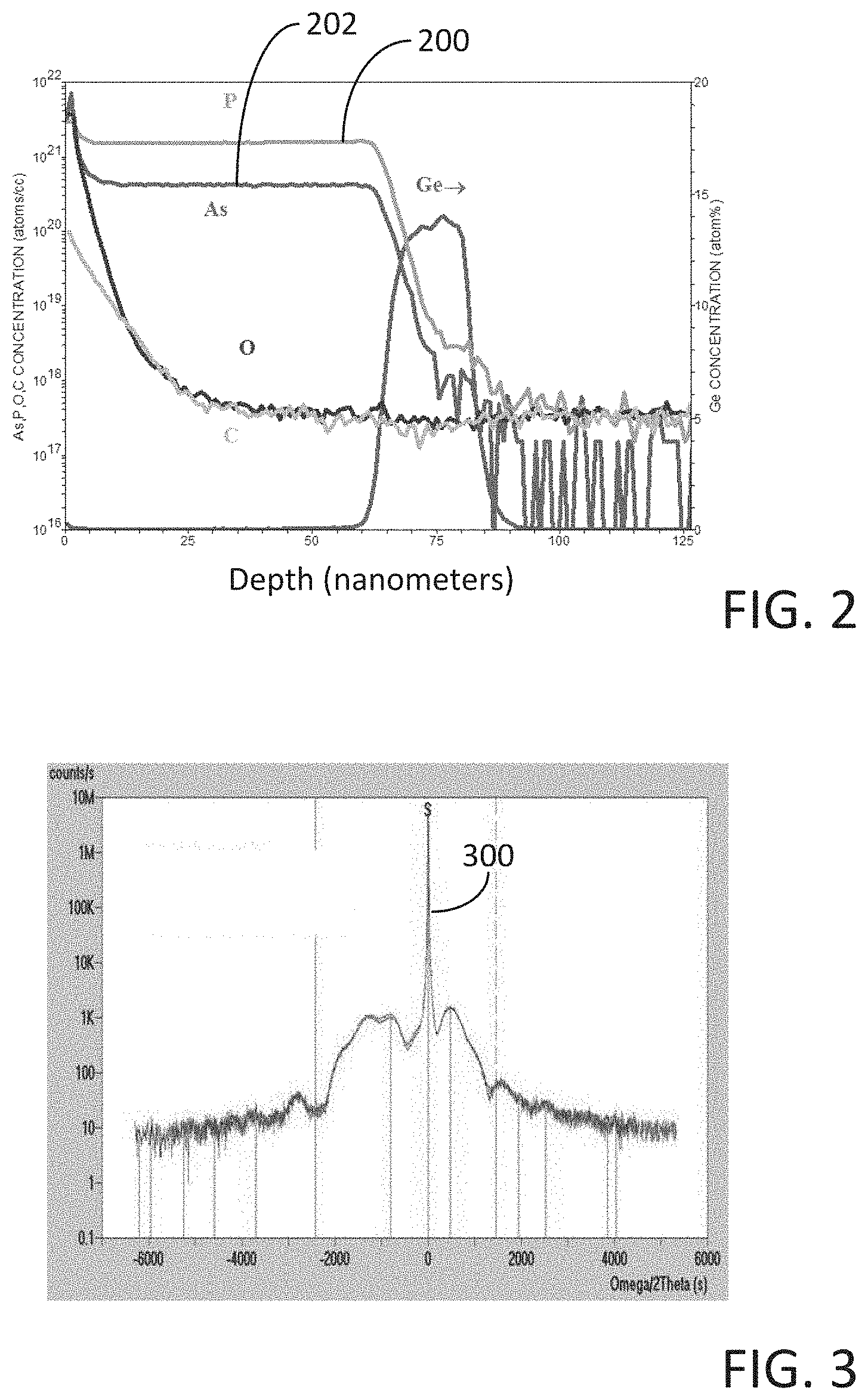
[0011] FIG. 2 illustrates a secondary ion mass spectrum (SIMS) obtain from a phosphorus doped silicon arsenide film deposited according to the embodiments of the disclosure;
[0012] FIG. 3 illustrates x-ray diffraction (XRD) data obtain from a phosphorus doped silicon arsenide film deposited according to the embodiments of the disclosure;
[0013] FIG. 4 illustrates a schematic diagram of a semiconductor device structure including a phosphorus doped silicon arsenide film in accordance with embodiments of the disclosure; and
[0014] FIG. 5 illustrates an additional schematic diagram of a semiconductor device structure including a phosphorus doped silicon arsenide film in accordance with the embodiments of the disclosure.
[0015] It will be appreciated that elements in the figures are illustrated for simplicity and clarity and have not necessarily been drawn to scale. For example, the dimensions of some of the elements in the figures may be exaggerated relative to other elements to help improve understanding of illustrated embodiments of the present disclosure.
DETAILED DESCRIPTION OF EXEMPLARY EMBODIMENTS
[0016] Although certain embodiments and examples are disclosed below, it will be understood by those in the art that the invention extends beyond the specifically disclosed embodiments and/or uses of the invention and obvious modifications and equivalents thereof. Thus, it is intended that the scope of the invention disclosed should not be limited by the particular disclosed embodiments described below.
[0017] As used herein, the term "substrate" may refer to any underlying material or materials that may be used, or upon which, a device, a circuit or a film may be formed.
[0018] As used herein, the term "phosphorus doped silicon arsenide" may refer to a material comprising both silicon species and arsenic species as well as active phosphorus dopant species.
[0019] As used herein, the term "film" and "thin film" may refer to any continuous or non-continuous structures and material deposited by the methods disclosed herein. For example, "film" and "thin film" could include 2D materials, nanorods, nanotubes, or nanoparticles or even partial or full molecular layers or partial or full atomic layers or clusters of atoms and/or molecules. "Film" and "thin film" may comprise material or a layer with pinholes, but still be at least partially continuous.
[0020] A number of example materials are given throughout the embodiments of the current disclosure, it should be noted that the chemical formulas given for each of the example materials should not be construed as limiting and that the non-limiting example materials given should not be limited by a given example stoichiometry.
[0021] The methods and related semiconductor device structures of the current disclosure may be utilized to deposit a phosphorus doped silicon arsenide film. In some embodiments, the phosphorus doped silicon arsenide film may be utilized as a diffusion barrier in the source/drain region of a transistor structure, to prevent diffusion of dopants from a highly doped silicon film disposed adjacent to the phosphorous doped silicon arsenide film.
[0022] In current CMOS technology the source/drain regions of the transistor device structure may comprise a highly phosphorus doped silicon film (e.g., phosphorus concentration of greater than 1.times.10.sup.21/cm) to enable a low resistance contact to be formed to the source/drain region of the device. However, the high concentration of phosphorus in the source/drain region must be contained to prevent diffusion of the phosphorus dopant into the active channel region of the device structure. Current technologies may utilize a silicon film with a low dopant concentration of phosphorus (e.g., a phosphorus concentration of less than 5.times.10.sup.20/cm.sup.3) to act as a diffusion barrier to the highly doped silicon film. However, in advanced technology nodes, as device geometries reduce and film thickness reduce, the ability of the low doped silicon film to prevent diffusion of dopants diminishes.
[0023] Silicon Arsenide (SiAs) may be utilized as an alternative diffusion barrier material in the source/drain regions. For example, arsenic diffuses less than phosphorus and therefore, source/drain regions formed with SiAs will have sharper and more abrupt junctions than those formed with a phosphorus doped silicon. However, current methods for depositing a SiAs film have been limited to SiAs films with an electrical resistivity of greater than 0.7 m.OMEGA.-cm. Accordingly, methods and related semiconductor device structures are desirable for depositing a low electrical resistivity silicon arsenide film.
[0024] Therefore, the methods of the disclosure may comprise methods for depositing a phosphorus doped silicon arsenide film. These methods may comprise: providing a substrate within a reaction chamber; heating the reaction chamber to a deposition temperature; exposing the substrate to a silicon precursor, an arsenic precursor, and a phosphorus dopant precursor; and depositing the phosphorus doped silicon arsenide film over a surface of the substrate.
[0025] The methods of the disclosure may be understood with reference to FIG. 1 which illustrates a non-limiting example embodiment of a method for depositing a phosphorus doped silicon arsenide film. The method 100 of forming a phosphorus doped silicon arsenide film may commence by means of a process block 110, which comprises providing a substrate into a reaction chamber and heating the substrate to a deposition temperature.
[0026] In some embodiments of the disclosure, the substrate may comprise a planar substrate or a patterned substrate. Patterned substrates may comprise substrates that may include semiconductor device structures formed into or onto a surface of the substrate; for example, the patterned substrates may comprise partially fabricated semiconductor device structures such as transistors and memory elements. A patterned substrate may comprise a non-planar surface which may comprise one or more fin structures extending up from the main surface of the substrate. The substrate may contain monocrystalline surfaces and/or one or more secondary surfaces that may comprise a non-monocrystalline surface, such as a polycrystalline surface and an amorphous surface. Monocrystalline surfaces may comprise, for example, one or more of: silicon (Si), silicon germanium (SiGe), germanium tin (GeSn), or germanium (Ge). Polycrystalline or amorphous surfaces may include dielectric materials, such as oxides, oxynitrides, or nitrides, including for example, silicon oxides and silicon nitrides.
[0027] As a non-limiting example, the reaction chamber may comprise a reaction chamber of a chemical vapor deposition system. However, it is also contemplated that other reaction chambers, such as, for example, atomic layer deposition reaction chambers, and alternative chemical vapor deposition systems may also be utilized to perform the embodiments of the present disclosure.
[0028] With continued reference to FIG. 1, the process block 110 of exemplary method 100 may continue by heating the substrate to a desired deposition temperature within a reaction chamber. In some embodiments of the disclosure, the method 100 may comprise heating the substrate to a temperature of less than approximately 750.degree. C., or to a temperature of less than approximately 650.degree. C., or to a temperature of less than approximately 600.degree. C., or to a temperature of less than approximately 550.degree. C., or even to a temperature of less than approximately 500.degree. C. For example, in some embodiments of the disclosure, heating the substrate to a deposition temperature may comprise heating the substrate to a temperature of between approximately 660.degree. C. and approximately 720.degree. C.
[0029] In addition to controlling the temperature of the substrate, the pressure within the reaction chamber may also be regulated. For example, in some embodiments of the disclosure, the pressure within the reaction chamber may be less than 300 Torr, or less than 250 Torr, or less than 200 Torr, or less than 150 Torr, or less than 100 Torr, or even less than 50 Torr. In some embodiments, the pressure in the reaction chamber may be between 50 Torr and 300 Torr.
[0030] Once the substrate is heated to the desired deposition temperature, the exemplary method 100 may continue by means of a process block 120 comprising, exposing the substrate to a silicon precursor, an arsenic precursor, and a phosphorus dopant precursor. In some embodiments, the substrate exposure to the silicon precursor, the arsenic precursor, and the phosphorus dopant precursor may occur concurrently, in other words, the silicon precursor, the arsenic precursor, and the phosphorus dopant precursor are co-flowed into the reaction chamber and interact with the heated substrate as a gas mixture comprising the silicon precursor, the arsenic precursor, and the phosphorus dopant precursor. In some embodiments, exposing the substrate to the silicon precursor, the arsenic precursor, and the phosphorous dopant precursor may comprise sequentially introducing the precursors into the reaction chamber, in other words, the precursors are separately and sequentially introduced into the reaction chamber and contact the substrate.
[0031] In some embodiments of the disclosure, the silicon precursor may comprise a hydrogenated silicon precursor selected from the group comprising: silane (SiH.sub.4), disilane (Si.sub.2H.sub.6), trisilane (Si.sub.3H.sub.8), or tetrasilane (Si.sub.4H.sub.10). In some embodiments of the disclosure, the silicon precursor may comprise a chlorinated silicon precursor selected from the group comprising: monochlorosilane (MCS), dichlorosilane (DCS), trichlorosilane (TCS), hexachlorodisilane (HCDS), octachlorotrisilane (OCTS), or silicon tetrachloride (STC). In some embodiments, exposing the substrate to the silicon precursor comprises flowing the silicon precursor into the reaction chamber at flow rate of less than 1000 sccm, or less than 750 sccm, or even less than 500 sccm.
[0032] In some embodiments of the disclosure, the arsenic precursor may comprise at least one of arsine (AsH.sub.3), or tertiary butyl arsine (TBA). In some embodiments, exposing the substrate to the arsenic precursor comprises, flowing the arsenic precursor into the reaction chamber at flow rate of less than 200 sccm, or less than 100 sccm, or less than 50 sccm, or even less than 25 sccm.
[0033] In some embodiments of the disclosure, the phosphorus dopant precursor may comprise at least one of phosphine (PH.sub.3), or tertiary butyl phosphine (TBP). In some embodiments, exposing the substrate to the phosphorus dopant precursor comprises, flowing the phosphorus dopant precursor into the reaction chamber at flow rate of less than 200 sccm, or less than 150 sccm, or less than 100 sccm, or less than 50 sccm, or even less than 25 sccm.
[0034] In addition to the silicon precursor, the arsenic precursor, and the phosphorus dopant precursor, one or more carrier gases may also be introduced into the reaction chamber to enable flow of precursors into the reaction chamber. For example, a carrier gas may comprise one or more of hydrogen (H.sub.2) or nitrogen (N.sub.2).
[0035] The exemplary method 100 may continue by means of a process block 130 comprising, depositing a phosphorus doped silicon arsenide film. In some embodiments, the phosphorus doped silicon arsenide film may have a phosphorus concentration of greater than 1.times.10.sup.20/cm.sup.3, or greater than 5.times.10.sup.20/cm.sup.3, or even greater than 1.times.10.sup.21/cm.sup.3. In some embodiments, the phosphorus doped silicon arsenide film may have an arsenic concentration of greater than 1.times.10.sup.20/cm.sup.3, or greater than 5.times.10.sup.20/cm.sup.3, or even greater than 1.times.10.sup.21/cm.sup.3. For example, FIG. 2 illustrates a secondary ion mass spectrum (SIMS) obtain from a phosphorus doped silicon arsenide film deposited according to the embodiments of the disclosure. The data labelled as 200 illustrates the concentration of phosphorus in the phosphorus doped silicon arsenide film which in this exemplary film is approximately 1.times.10.sup.21/cm.sup.3. The data labelled as 202 illustrates the concentration of arsenic in the phosphorus doped silicon arsenide film which in this exemplary film is approximately 4.times.10.sup.20/cm.sup.3.
[0036] In some embodiments, the phosphorus doped silicon arsenide film may have an electrical resistivity of less than 0.9 m.OMEGA.-cm, or less than 0.7 m.OMEGA.-cm, or less than 0.5 m.OMEGA.-cm, or even less than 0.3 m.OMEGA.-cm.
[0037] In some embodiments, the phosphorus doped silicon arsenide film may be deposited to a thickness of less than 500 Angstroms, or less than 300 Angstroms, of less than 200 Angstroms, or less than 100 Angstroms, or less than 50 Angstroms, or even less than 25 Angstroms. In some embodiments of the disclosure, the phosphorus doped silicon arsenide may be deposited to a thickness between 100 Angstroms and 500 Angstroms.
[0038] In some embodiments of the disclosure, the phosphorus doped silicon arsenide film may be deposited as a crystalline material. For example, FIG. 3 illustrates x-ray diffraction (XRD) data obtained from a phosphorus doped silicon arsenide film deposited according to the embodiments of the disclosure. The XRD data of FIG. 3 shows a significant peak, labelled as 300, indicating the phosphorus doped silicon arsenide film is crystalline.
[0039] The embodiments of the disclosure may also provide semiconductor device structures comprising a phosphorus doped silicon arsenide film deposited according to the embodiments of the disclosure. For example, FIG. 4 illustrates a non-limiting example of a semiconductor device structure 400, wherein the semiconductor device structure 400 comprises a double gate MOSFET, commonly referred to as a FinFET. The semiconductor device structure 400 may comprise a substrate 402, which may comprise a bulk silicon (Si) substrate. The substrate 402 may be doped with p-type dopants (for NMOS type FinFET devices) and/or with n-type dopants (for PMOS type FinFET devices). In the non-limiting example semiconductor device structure of FIG. 4 the substrate 400 may comprise p-type dopants and the semiconductor device structure 400 may comprise an NMOS FinFET.
[0040] The semiconductor device structure 400 may also comprise isolation regions 404, which may comprise shallow trench isolation (STI) regions. The semiconductor device structure 400 may also comprise a Fin structure 406 extending over the top surfaces of the isolation regions 404, the portion of Fin structure 406 buried beneath additional device layers is shown by the dashed lines and particularly includes the channel region 412. A gate dielectric may be disposed over the sidewalls of the Fin structure 406 (not shown) and the gate dielectric may comprise a silicon oxide or a high-k dielectric material. A gate electrode 408 may be disposed on the gate dielectric for providing electrical contact to the channel region 412, the channel region 412 being the portion of the Fin structure 406 covered by the gate dielectric and the gate electrode. The semiconductor device structure 400 may also comprise gate spacers 410, which are disposed on the sidewalls of the gate electrode 408.
[0041] In some embodiments of the disclosure, the semiconductor device structure 400 may further comprise source/drain regions 414 disposed over the Fin structure 406 and adjacent to the channel region 412. In some embodiments, the source/drains regions 414 may comprise a phosphorus doped silicon arsenide film 416 deposited according to the embodiments of the disclosure, and a doped silicon film 418, such as, for example, a phosphorus doped silicon film. It should be noted that the source/drain regions 414 comprising the phosphorus doped silicon arsenide film 416 and the doped silicon film 418 may comprise a number of facets that may result due to the difference in growth rates on the different facets of the Fin structure 406.
[0042] Therefore, in some embodiments of the disclosure, the phosphorus doped silicon arsenide film 416 may be deposited adjacent to a channel region 412 of a semiconductor device structure and the methods may further comprise depositing a doped silicon film 418 adjacent to the phosphorus doped silicon arsenide film 416. For example, the phosphorus doped silicon arsenide film 416 may be deposited directly over the Fin structure 406 in the source/drain regions 414, adjacent to the channel region 412. A doped silicon film 418 may be deposited directly over the phosphorus doped silicon arsenide film, wherein the doped silicon film may comprise a phosphorus doped silicon film. Therefore in some embodiments, the phosphorus doped silicon arsenide film 416 may be deposited between a phosphorus doped silicon film 418 with a phosphorus concentration greater than 1.times.10.sup.21/cm.sup.3 and a channel region 412 of a semiconductor device, wherein the phosphorus doped silicon arsenide film 416 is a diffusion barrier to prevent phosphorus dopants from the phosphorus doped silicon film 418 form diffusing into the channel region 412.
[0043] The embodiments of the disclosure therefore provide semiconductor device structures including a phosphorus doped silicon arsenide film. In some embodiments the semiconductor device structure, such as device structure 400, may comprise: a channel region 412, a phosphorus doped silicon arsenide film 416 disposed adjacent to the channel region 412, and a doped silicon film 418 disposed adjacent to the phosphorus doped silicon arsenide film 416, wherein the phosphorus doped silicon arsenide film 416 is disposed between the channel region 412 and the doped silicon film 418 and substantially prevents the diffusion of dopants from the doped silicon film 418 into the channel region 412. In some embodiments, the phosphorus doped silicon arsenide film 416 is disposed directly between the channel region 412 and the doped silicon film 418. In some embodiments, the phosphorus doped silicon arsenide film 416 may have a phosphorus concentration of greater than 5.times.10.sup.20/cm.sup.3. In some embodiments, the phosphorus doped silicon arsenide film 416 may have an arsenic concentration of greater than 5.times.10.sup.20/cm.sup.3. In some embodiments, the phosphorus doped silicon arsenide film 416 may have an electrical resistivity of less than 0.9 m.OMEGA.-cm, or less than 0.5 m.OMEGA.-cm, or less than 0.3 m.OMEGA.-cm. In some embodiments, the phosphorus doped silicon arsenide film 416 may have a thickness of less than 500 Angstroms. In addition, in some embodiments, the doped silicon film 418 may comprise a phosphorus doped silicon film with a phosphorus concentration greater than 1.times.10.sup.21/cm.sup.3.
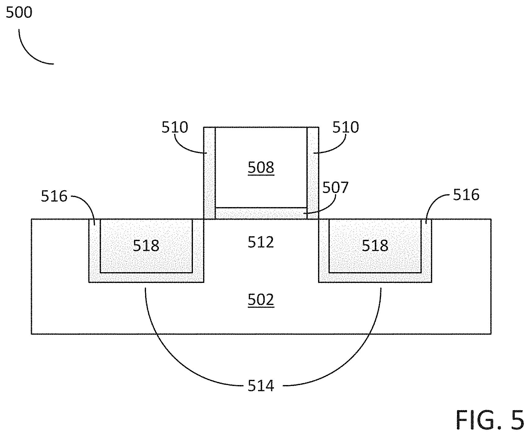
[0044] A further example of semiconductor device structure that may employ a phosphorus doped silicon arsenide film is illustrated in FIG. 5. In more detail, FIG. 5 illustrates semiconductor device structure 500, which may comprise a planar NMOS FET device. Semiconductor device structure may include a substrate 502, which may include p-type dopants. Disposed in the or on the substrate are source/drain regions 514, the source/drain regions 514 comprising a phosphorus doped silicon arsenide film 516 and a phosphorus doped silicon film 518. A channel region 512 may be disposed between the source/drain regions 505 and a gate dielectric 507 and gate electrode 508 may be disposed over the channel region 512. In addition, gate spacers 510 may be disposed over the substrate 502. Therefore, semiconductor device structure 500 comprises, a channel region 512, a phosphorus doped silicon arsenide film 516 disposed adjacent to the channel region 512, and a doped silicon film 518 disposed adjacent to the phosphorus doped silicon arsenide film 516. The phosphorus doped silicon arsenide film 516 is disposed between the channel region 512 and the doped silicon film 518 and substantially prevents diffusion of dopants from the doped silicon film 518 into the channel region 512.
[0045] In some embodiments of the disclosure, an electrical contact may be made to the source/drain regions 414, 514 of the FET devices illustrated in FIGS. 4 and 5. In some embodiments, the electrical contact (not shown) may comprise a silicide, such as, for example, a titanium silicide (TiSi.sub.2). The embodiments of the disclosure allow for a high concentration of active n-type carriers in the source/drain regions 414 and 514, which in turn may result in a reduction in the electrical contact resistance to the source/drain regions. For example, the methods of the disclosure may comprise forming an electrical contact to the source/drain regions 414 and 514, wherein the electrical contact has an electrical resistivity of less than 0.9 m.OMEGA.-cm, or less than 0.5 m.OMEGA.-cm, or even less than 0.3 m.OMEGA.-cm.
[0046] The example embodiments of the disclosure described above do not limit the scope of the invention, since these embodiments are merely examples of the embodiments of the invention, which is defined by the appended claims and their legal equivalents. Any equivalent embodiments are intended to be within the scope of this invention. Indeed, various modifications of the disclosure, in addition to those shown and described herein, such as alternative useful combination of the elements described, may become apparent to those skilled in the art from the description. Such modifications and embodiments are also intended to fall within the scope of the appended claims.
* * * * *
D00000
D00001
D00002
D00003
D00004
XML
uspto.report is an independent third-party trademark research tool that is not affiliated, endorsed, or sponsored by the United States Patent and Trademark Office (USPTO) or any other governmental organization. The information provided by uspto.report is based on publicly available data at the time of writing and is intended for informational purposes only.
While we strive to provide accurate and up-to-date information, we do not guarantee the accuracy, completeness, reliability, or suitability of the information displayed on this site. The use of this site is at your own risk. Any reliance you place on such information is therefore strictly at your own risk.
All official trademark data, including owner information, should be verified by visiting the official USPTO website at www.uspto.gov. This site is not intended to replace professional legal advice and should not be used as a substitute for consulting with a legal professional who is knowledgeable about trademark law.