Nonfouling Biosensors
Chilkoti; Ashutosh ; et al.
U.S. patent application number 16/305696 was filed with the patent office on 2020-12-03 for nonfouling biosensors. The applicant listed for this patent is Duke University. Invention is credited to Roozbeh Abedini-Nassab, Joseph Andrews, Ashutosh Chilkoti, Aaron Franklin, Angus Hucknall, Daniel Joh, Benjamin Yellen.
| Application Number | 20200378916 16/305696 |
| Document ID | / |
| Family ID | 1000005085466 |
| Filed Date | 2020-12-03 |


View All Diagrams
| United States Patent Application | 20200378916 |
| Kind Code | A1 |
| Chilkoti; Ashutosh ; et al. | December 3, 2020 |
NONFOULING BIOSENSORS
Abstract
Disclosed are sensors that include a carbon nanotube channel and a non-fouling polymer layer, where the non-fouling polymer layer and the carbon nanotube channel do not directly contact each other and are separated by a dielectric layer. The disclosed sensors may be used, e.g., as biosensors for the accurate and sensitive detection of analytes within a sample. Also disclosed are methods of making and using the sensors.
| Inventors: | Chilkoti; Ashutosh; (Durham, NC) ; Franklin; Aaron; (Durham, NC) ; Yellen; Benjamin; (Durham, NC) ; Hucknall; Angus; (Durham, NC) ; Joh; Daniel; (Durham, NC) ; Abedini-Nassab; Roozbeh; (Durham, NC) ; Andrews; Joseph; (Durham, NC) | ||||||||||
| Applicant: |
|
||||||||||
|---|---|---|---|---|---|---|---|---|---|---|---|
| Family ID: | 1000005085466 | ||||||||||
| Appl. No.: | 16/305696 | ||||||||||
| Filed: | June 1, 2017 | ||||||||||
| PCT Filed: | June 1, 2017 | ||||||||||
| PCT NO: | PCT/US17/35530 | ||||||||||
| 371 Date: | November 29, 2018 |
Related U.S. Patent Documents
| Application Number | Filing Date | Patent Number | ||
|---|---|---|---|---|
| 62343926 | Jun 1, 2016 | |||
| 62414877 | Oct 31, 2016 | |||
| Current U.S. Class: | 1/1 |
| Current CPC Class: | G01N 27/126 20130101; G01N 33/5438 20130101; G01N 27/127 20130101; G01N 27/227 20130101 |
| International Class: | G01N 27/22 20060101 G01N027/22; G01N 33/543 20060101 G01N033/543; G01N 27/12 20060101 G01N027/12 |
Claims
1. A sensor comprising: a conductive substrate; a first dielectric layer positioned on the conductive substrate; a carbon nanotube channel comprising at least one carbon nanotube, the carbon nanotube channel being positioned on the first dielectric layer; a source electrode and a drain electrode positioned on the carbon nanotube channel; a second dielectric layer positioned on the carbon nanotube channel; a non-fouling polymer layer comprising hydroxy terminated poly oligo(ethylene glycol) methyl methacrylate (POEGMA), alkoxy terminated POEGMA, a copolymer of alkoxy-terminated POEGMA and hydroxy-terminated POEGMA, or a combination thereof, the non-fouling polymer layer being positioned on the second dielectric layer; and at least one capture agent adapted to specifically bind to a target analyte, the capture agent being bound to the non-fouling polymer layer.
2. The sensor of claim 1, wherein the conductive substrate comprises silicon, doped silicon, a III-V group semiconductor substrate, a II-VI group semiconductor substrate, an epitaxially grown silicon-germanium substrate, a glass substrate, a quartz substrate, a metal substrate or a plastic substrate.
3. The sensor of claim 1, wherein at least one of the first and second dielectric layers comprise a metal oxide.
4. The sensor of claim 3, wherein the metal oxide comprises SiO.sub.2, Sc.sub.2O.sub.3, Al.sub.2O.sub.3, TiO.sub.2, MgO, In.sub.2O.sub.3, SnO.sub.2, ZnO, ZnMgO, or a combination thereof.
5. The sensor of claim 1, wherein the first dielectric layer has a thickness of from about 10 nm to about 500 nm.
6. The sensor of claim 1, wherein the second dielectric layer has a thickness of from about 10 nm to about 30 nm.
7. The sensor of claim 1, wherein the carbon nanotube channel has a thickness of from about 1 nm to about 10 nm.
8. The sensor of claim 1, wherein the carbon nanotube channel is printed onto the first dielectric layer.
9. The sensor of claim 1, wherein the carbon nanotube channel comprises a plurality of carbon nanotubes.
10. The sensor of claim 1, wherein the carbon nanotube is semi-conducting.
11. The sensor of claim 1, wherein the non-fouling polymer layer has a thickness of from about 10 nm to about 150 nm.
12. The sensor of claim 1, wherein the non-fouling polymer layer has an ethylene glycol repeat unit of greater than or equal to 2.
13. The sensor of claim 1, wherein the non-fouling polymer layer does not directly contact the carbon nanotube channel.
14. The sensor of claim 1, wherein the capture agent is non-covalently bound to the non-fouling polymer layer.
15. The sensor of claim 1, wherein the capture agent is separated from the carbon nanotube channel by a distance of greater than 5 nm.
16. The sensor of claim 1, further comprising a detection agent adapted to specifically bind to a target analyte.
17. The sensor of claim 1, wherein at least one of the capture agent and detection agent comprises a nucleic acid, a carbohydrate, a protein or a peptide.
18. The sensor of claim 17, wherein the protein is an antibody.
19. The sensor of claim 18, wherein the antibody is printed onto the non-fouling polymer layer.
20. The sensor of claim 1, further comprising an electronic circuit configured to measure an electrical property of the carbon nanotube channel.
21. The sensor of claim 20, wherein the electrical property is selected from the group consisting of resistivity, capacitance, impedance, inductance, and a combination thereof.
22. A method of detecting the presence or absence of an analyte, the method comprising: contacting the sensor of claim 1 with a sample; measuring an electrical property of the carbon nanotube channel; and determining the presence of the analyte, wherein the presence of the analyte is detected through a change in the electrical property of the carbon nanotube channel upon binding of the analyte to the capture agent.
23. The method of claim 22, wherein the sample does not directly contact the carbon nanotube channel.
Description
CROSS-REFERENCE TO RELATED APPLICATIONS
[0001] This application claims priority to U.S. Provisional Application No. 62/343,926 filed on Jun. 1, 2016, and U.S. Provisional Application No. 62/414,877 filed on Oct. 31, 2016, both of which are incorporated fully herein by reference.
BACKGROUND
[0002] Printed electronics is a rapidly expanding field as it offers easy integration into current manufacturing processes, is inherently low-cost, and enables rapid fabrication of large-area sensors for use in Internet-of-Things (IoT) technologies. Recently, nanomaterials have provided a viable path forward for printed electronics, especially with the commercial availability of solution-processed semiconducting carbon nanotubes (CNTs). Printed CNT thin-film transistors (TFTs) have shown high performance, while remaining robust to the environment, unlike the more traditional printed organic semiconductors. CNTs have also proven useful in highly sensitive biosensor applications, where small changes in charge in the vicinity of the CNTs can produce a sizeable electrical response. Nonetheless, there is still a need for improved CNT-based biosensors that can accurately and sensitively detect analytes in a biological milieu without, e.g., rinsing or pre-sample calibration.
SUMMARY
[0003] In one aspect, disclosed are sensors that include a conductive substrate; a first dielectric layer positioned on the conductive substrate; a carbon nanotube channel comprising at least one carbon nanotube, the carbon nanotube channel being positioned on the first dielectric layer; a source electrode and a drain electrode positioned on the carbon nanotube channel; a second dielectric layer positioned on the carbon nanotube channel; a non-fouling polymer layer comprising hydroxy terminated poly oligo(ethylene glycol) methyl methacrylate (POEGMA), alkoxy terminated POEGMA, a copolymer of alkoxy-terminated POEGMA and hydroxy-terminated POEGMA, or a combination thereof, the non-fouling polymer layer being positioned on the second dielectric layer; and at least one capture agent adapted to specifically bind to a target analyte, the capture agent being bound to the non-fouling polymer layer.
[0004] In another aspect, disclosed are methods of detecting the presence or absence of an analyte. The methods include contacting the disclosed sensor with a sample; measuring an electrical property of the carbon nanotube channel; and determining the presence of the analyte, wherein the presence of the analyte is detected through a change in the electrical property of the carbon nanotube channel upon binding of the analyte to the capture agent.
BRIEF DESCRIPTION OF THE DRAWINGS
[0005] FIG. 1 is a schematic showing Poly oligo(ethylene glycol) methyl ether methacrylate (POEGMA) brush growth from dielectric oxide materials by surface-initiated atom transfer radical polymerization (SI-ATRP).
[0006] FIG. 2 is a set of graphs showing growth behavior of POEGMA brushes grown by SI-ATRP on metal oxides. POEGMA brush growth was measured by reflective mode ellipsometry at the indicated timepoints for (A) Si/SiO.sub.2, (B) TiO.sub.2, (C) ZrO.sub.2, and (D) Al.sub.2O.sub.3.
[0007] FIG. 3 is a graph showing the effect of bromide initiator on POEGMA brush growth.
[0008] FIG. 4 A-D is a set of graphs showing X-ray photoelectron spectra prior to and after SI-ATRP on metal oxides. (A & B): survey spectra of initiator-grafted (APTES-BiB) surfaces on Si/SiO.sub.2 and TiO.sub.2, respectively. (C & D): survey spectra following SI-ATRP of POEGMA brushes. Insets: High resolution C1s spectra following SI-ATRP, showing peaks consistent with POEGMA brushes following peak fitting.
[0009] FIG. 5 A-D is a set of graphs showing X-ray photoelectron spectra prior to and after SI-ATRP on metal oxides. (A & B): survey spectra of initiator-grafted (APTES-BiB) surfaces on ZrO.sub.2 and Al.sub.2O.sub.3, respectively. (C & D): survey spectra following SI-ATRP of POEGMA brushes. Insets: High resolution C1s spectra following SI-ATRP, showing peaks consistent with POEGMA brushes following peak fitting.
[0010] FIG. 6 is a schematic of the POEGMA samples used to obtain the capacitance-voltage curves with detailed expression for the total measured capacitance (C.sub.meas) used for determining permittivity.
[0011] FIG. 7 is a set of graphs showing capacitance-voltage measurements on POEGMA. (A-C): sequence of capacitance-voltage curves from a POEGMA film of 24.3 nm thickness beginning with the initial characteristic (A), followed by the response post-hydration of the POEGMA (B), and finally after a drying step to dehydrate (C). (D): linear fit to plot of the inverse POEGMA capacitance versus thickness used to confirm the extracted permittivity Ep.
[0012] FIG. 8 is (A): a schematic of a POEGMA sample used to investigate the breakdown of POEGMA films. (B): is a graph showing the breakdown curve for a POEGMA film of 44.2 nm thick.
[0013] FIG. 9 is a set of fluorescence images of adsorption of Cy5-BSA onto dielectric metal oxide surfaces with and without POEGMA coatings. Images of SiO.sub.2 surfaces (with and without POEGMA) treated with PBS vehicle also shown as negative control.
[0014] FIG. 10 is the quantitation of fluorescence from residual Cy5-BSA bound to surfaces at the conditions described in FIG. 9; data are average .+-.s.d. of 3 separate chips. Inset: magnified view of low fluorescence intensity data.
[0015] FIG. 11 is a schematic of printed substrate gate CNT-thin filmed transistor (CNT-TFT) profile without a second dielectric layer in between the carbon nanotube channel and the non-fouling polymer layer. Optical images (with a 100 .mu.m scale bar) show sensors before POEGMA step and after printed biologicals.
[0016] FIG. 12 is a schematic of a sensor that applies Al.sub.2O.sub.3 via atomic layer deposition (ALD).
[0017] FIG. 13 is a plot of subthreshold curves of a sensor before and after atomic layer deposition of a dielectric layer onto the carbon nanotube channel.
[0018] FIG. 14 is a plot of transfer curves of a sensor before and after atomic layer deposition of a dielectric layer onto the carbon nanotube channel.
[0019] FIG. 15 is a schematic of a sensor including a second dielectric layer positioned in between the non-fouling polymer layer and the carbon nanotube channel, as well as capture and detections agents printed onto the non-fouling polymer layer.
[0020] FIG. 16 is a photograph of a fabricated device.
[0021] FIG. 17 is a plot of forward gate voltage swings (only) for a sensor (with a second dielectric layer) exposed to a sample including leptin.
[0022] FIG. 18 is a plot of forward gate voltage swings to -1V for a sensor (with a second dielectric layer) exposed to a sample including leptin.
[0023] FIG. 19 is a plot of subthreshold curve forward gate voltage sweep for a sensor (with a second dielectric layer) exposed to a sample including leptin.
[0024] FIG. 20 is a schematic of printed substrate gate CNT-thin filmed transistor (CNT-TFT) profile without a second dielectric layer in between the carbon nanotube channel and the non-fouling polymer layer. Optical images (with a 100 .mu.m scale bar) show sensors before POEGMA step and after printed biologicals.
[0025] FIG. 21 is a schematic of how the sensors can be used to detect the presence (or absence) of an analyte within a sample.
[0026] FIG. 22 is a schematic of a sensor that has the non-fouling polymer layer directly contacting the carbon nanotube channel, as well as capture and detection agents printed onto the non-fouling polymer layer.
[0027] FIG. 23 is a photograph of a fabricated sensor.
[0028] FIG. 24 is a plot of transfer (linear) curves of a sensor (without a second dielectric layer) before and after POEGMA growth.
[0029] FIG. 25 is a plot of subthreshold (log-scale) curves of a sensor (without a second dielectric layer) before and after POEGMA growth.
[0030] FIG. 26 is a plot of transfer (linear) curves of a sensor (without a second dielectric layer) exposed to a sample including leptin.
[0031] FIG. 27 is a plot of subthreshold (log-scale) curves of a sensor (without a second dielectric layer) exposed to a sample including leptin.
[0032] FIG. 28 is a schematic of a method for using the disclosed sensors to detect the presence (or absence) of an analyte in a sample.
[0033] FIG. 29 is a plot showing that the charge from antibodies causes a shift in the threshold voltage (turn-on voltage) and the transconductance of the transistor (where the sensor has a second dielectric layer).
[0034] FIG. 30 is (a) a schematic of printed substrate gate CNT-TFT profile without a second dielectric layer in between the carbon nanotube channel and the non-fouling polymer layer; (b) optical image with a 100 .mu.m scale bar; (c) SEM image at 25,000.times. magnification of silver nanoparticle source/drain; (d) SEM image at 350,000.times. magnification of CNT channel.
[0035] FIG. 31 is a plot of a subthreshold for a printed substrate gated CNT-TFT (lacking a second dielectric layer).
[0036] FIG. 32 is a plot of a transfer characteristics for a printed substrate gated CNT-TFT (lacking a second dielectric layer).
[0037] FIG. 33 is a plot of transfer characteristics of a sensor (with a second dielectric layer) following being contacted with a sample that includes leptin.
[0038] FIG. 34 is a plot of normalized on-current as a function of leptin concentration (where the sensor has a second dielectric layer).
[0039] FIG. 35 is a plot of dose response curves normalized to pre-serum on-current across a sensor (with a second dielectric layer), each sensor measured individually.
[0040] FIG. 36 is a plot of dose response curves normalized to pre-serum on-current across a sensor (with a second dielectric layer), the average of the three sensors shown.
DETAILED DESCRIPTION
[0041] Disclosed herein are biosensors that show advantageous accuracy and sensitivity of detection of target analytes in biological samples. The biosensors include a POEGMA-based non-fouling polymer layer and a printed carbon nanotube thin-filmed transistor, where a dielectric layer is positioned in between the carbon nanotube thin film and the POEGMA layer. The biosensors can detect the presence (or absence) of an analyte through binding interactions between the target analyte and capture agent(s) printed, non-covalently onto the POEGMA layer, which can then result in a change of an electrical property of the carbon nanotube thin-filmed transistor.
[0042] It was found that POEGMA can be synthesized onto metal oxide surfaces--in particular, high-permittivity ("high-.kappa.") metal oxide dielectrics, and that POEGMA can function as a dielectric, thereby permitting the biosensors to maintain good electrical conductivity, while also having the advantage of POEGMA's non-fouling property. Furthermore, it was found that POEGMA has a high breakdown voltage characteristic, which allows the disclosed biosensors to function up to high voltages.
[0043] In addition, it was found that a more robust and reliable sensor can be provided when there is a dielectric layer positioned in between the POEGMA layer and the carbon nanotube transistor film. It is well-recognized in the art that it is desirable to have the capture agent as close to the carbon nanotube film as possible, as the closer proximity can achieve a greater change in signal due to the binding event between the capture agent and the target analyte. For example, Kim et al., "Ultrasensitive carbon nanotube-based biosensors using antibody-binding fragments," Anal. Biochem., vol. 381, no. 2, pp. 193-198, 2008, which is incorporated by reference herein in its entirety, found that proximity (e.g., Debeye length in this instance) of the capture agent to the CNT channel impacted the overall sensitivity of the sensor. Specifically, Kim et al. found that smaller fragments of the capture agent (e.g., fragment of an antibody) were able to sense concentrations at a lower limit of 1 pg/ml IgG, while the larger full antibodies had a lower limit of approximately 1000 ng/ml IgG. In fact, they suggested that the Debye length is approximately 3 nm in a 10 mM buffer solution, and that the capture agents must fit in this range to electrostatically alter the CNT channel in order to modulate the conductance. Yet, it has been found with the disclosed sensors that the capture agent does not have to be in direct contact or in relatively close proximity to the carbon nanotube channel to achieve sensitive and accurate detection of a target analyte. Rather, sensitive detection can still be achieved when at least a dielectric layer is positioned in between the capture agent and the carbon nanotube film.
[0044] The advantages of the disclosed biosensors have been demonstrated through the detection of leptin within a serum sample down to a concentration of 10 pg/ml, with a detection range of 10.sup.5. Moreover, the biosensors needs calibration only with the dry transistor characteristics, furthering its viability as a real world, commercial biosensor application.
1. Definitions
[0045] Unless otherwise defined, all technical and scientific terms used herein have the same meaning as commonly understood by one of ordinary skill in the art. In case of conflict, the present document, including definitions, will control. Preferred methods and materials are described below, although methods and materials similar or equivalent to those described herein can be used in practice or testing of the present invention. All publications, patent applications, patents and other references mentioned herein are incorporated by reference in their entirety. The materials, methods, and examples disclosed herein are illustrative only and not intended to be limiting.
[0046] The terms "comprise(s)," "include(s)," "having," "has," "can," "contain(s)," and variants thereof, as used herein, are intended to be open-ended transitional phrases, terms, or words that do not preclude the possibility of additional acts or structures. The singular forms "a," "an" and "the" include plural references unless the context clearly dictates otherwise. The present disclosure also contemplates other embodiments "comprising," "consisting of" and "consisting essentially of," the embodiments or elements presented herein, whether explicitly set forth or not.
[0047] The conjunctive term "or" includes any and all combinations of one or more listed elements associated by the conjunctive term. For example, the phrase "an apparatus comprising A or B" may refer to an apparatus including A where B is not present, an apparatus including B where A is not present, or an apparatus where both A and B are present. The phrases "at least one of A, B, . . . and N" or "at least one of A, B, . . . N, or combinations thereof" are defined in the broadest sense to mean one or more elements selected from the group comprising A, B, . . . and N, that is to say, any combination of one or more of the elements A, B, . . . or N including any one element alone or in combination with one or more of the other elements which may also include, in combination, additional elements not listed.
[0048] The modifier "about" used in connection with a quantity is inclusive of the stated value and has the meaning dictated by the context (for example, it includes at least the degree of error associated with the measurement of the particular quantity). The modifier "about" should also be considered as disclosing the range defined by the absolute values of the two endpoints. For example, the expression "from about 2 to about 4" also discloses the range "from 2 to 4." The term "about" may refer to plus or minus 10% of the indicated number. For example, "about 10%" may indicate a range of 9% to 11%, and "about 1" may mean from 0.9-1.1. Other meanings of "about" may be apparent from the context, such as rounding off, so, for example "about 1" may also mean from 0.5 to 1.4.
[0049] The term "alkoxy" as used herein, refers to a radical of the formula R--O--, wherein R is a straight-chain or branched alkyl group having from 1 to 20, in particular 1 to 4 carbon atoms. Examples include methoxy, ethoxy, n-propoxy, iso-propoxy, n-butoxy, 2-butoxy, iso-butoxy (2-methylpropoxy), tert.-butoxy pentyloxy, 1-methylbutoxy, 2-methylbutoxy, 3-methylbutoxy, 2,2-dimethylpropoxy, 1-ethylpropoxy, hexyloxy, 1,1-dimethylpropoxy, 1,2-dimethylpropoxy, 1-methylpentyloxy, 2-methylpentyloxy, 3-methylpentyloxy, 4-methylpentyloxy, 1,1-dimethylbutoxy, 1,2-dimethylbutoxy, 1,3-dimethylbutoxy, 2,2-dimethylbutoxy, 2,3-dimethylbutoxy, 3,3-dimethylbutoxy, 1-ethylbutoxy, 2-ethylbutoxy, 1,1,2-trimethylpropoxy, 1,2,2-trimethylpropoxy, 1-ethyl-1-methylpropoxy and 1-ethyl-2-methylpropoxy.
2. Sensors
[0050] Disclosed herein are sensors that include a multi-layered structure. The sensor includes a conductive substrate, a first dielectric layer, a carbon nanotube channel, a second dielectric layer, a non-fouling polymer layer and at least one capture agent. FIG. 15 shows an embodiment of the sensor, where the conductive substrate serves as the base of the sensor, and the first dielectric layer, carbon nanotube channel, second dielectric layer, and non-fouling polymer layer are positioned above the substrate in that order (e.g., bottom: conductive substrate--top: non-fouling polymer layer). The sensors can be used to accurately detect whether an analyte is present within a sample, e.g., a biological sample. In some embodiments, the sensor can be a field effect transistor sensor.
A. Conductive Substrate
[0051] The sensor includes a conductive substrate. The conductive substrate may serve as the base of the sensor. The conductive substrate may act as a gate of the sensor, where voltage is applied. Accordingly, the conductive substrate can be configured to have a voltage applied to it. The conductive substrate may include any suitable material that allows the disclosed sensors to perform their intended function, e.g., the substrate may be any material that can be configured to have a voltage applied thereto, while also being able to electrostatically affect and/or control the carbon nanotube channel. Examples include, but are not limited to, silicon, doped silicon, a III-V group semiconductor substrate, a II-VI group semiconductor substrate, an epitaxially grown silicon-germanium substrate, a glass substrate, a quartz substrate, a metal substrate or a plastic substrate. In some embodiments, the conductive substrate may include p-doped silicon. In some embodiments, the conductive substrate may consist of doped silicon. In some embodiments, the conductive substrate may be p-doped silicon.
[0052] The conductive substrate may have a varying thickness. For example, the conductive substrate may have a thickness of from about 10 nm to about 20 .mu.m, such as from about 100 nm to about 10 .mu.m, or from about 500 nm to about 10 82 m.
B. Dielectric Layers
[0053] The sensor includes a first dielectric layer and a second dielectric layer. The dielectric layers are positioned in different locations of the sensor. The first dielectric layer is positioned on the conductive substrate, and is between the conductive substrate and the carbon nanotube channel. The second dielectric layer is positioned on the carbon nanotube channel, and is between the carbon nanotube channel and the non-fouling polymer layer. The first and second dielectric layers may directly contact each other, but the first dielectric layer may not directly contact the non-fouling polymer layer, and the second dielectric layer may not directly contact the conductive substrate.
[0054] The dielectric layers may include any suitable dielectric material known within the art that allows the sensor to perform its intended function. In some embodiments, at least one of the first and second dielectric layers may include a metal oxide. In some embodiments, the first and second dielectric layers may both include a metal oxide. Further, in some embodiments the first and second dielectric layers may each independently consist essentially of a metal oxide. In still further embodiments, the first and second dielectric layers may each independently consist of a metal oxide. In embodiments where the first and second dielectric layers both include a metal oxide, the dielectric layers may include the same metal oxide, or they may include different metal oxides. Examples of metal oxides include, but are not limited to, SiO.sub.2, Sc.sub.2O.sub.3, Al.sub.2O.sub.3, TiO.sub.2, MgO, In.sub.2O.sub.3, SnO.sub.2, ZnO, ZnMgO, or any combination thereof. In some embodiments, the first dielectric layer includes SiO.sub.2. In some embodiments, the second dielectric layer may include Al.sub.2O.sub.3.
[0055] The first and second dielectric layers may each independently have a varying thickness. For example, the first dielectric layer may have a thickness of from about 10 nm to about 500 nm, such as from about 50 nm to about 400 nm or from about 100 nm to about 350 nm. In some embodiments, the first dielectric layer may have a thickness of greater than 10 nm, greater than 50 nm, greater than 100, greater than 150 nm, or greater than 200 nm. In some embodiments, the first dielectric layer may have a thickness of less than 500 nm, less than 450 nm, less than 400 nm, or less than 350 nm.
[0056] In addition, the second dielectric layer may have a thickness of from about 5 nm to about 50 nm, such as from about 10 nm to about 40 nm, from about 10 nm to about 30 nm, or from about 10 nm to about 25 nm. In some embodiments, the second dielectric layer may have a thickness of greater than 5 nm, greater than 6 nm, greater than 7 nm, greater than 8 nm, greater than 9 nm, greater than 10 nm, greater than 15 nm, greater than 20 nm, or greater than 25 nm. In some embodiments, the second dielectric layer may have a thickness of less than 50 nm, less than 45 nm, less than 40 nm, less than 35 nm, or less than 30 nm.
[0057] In some embodiments, the second dielectric layer may have a thickness less than that of the first dielectric layer. For example, the second dielectric layer may have a thickness of about 20 nm, while the first dielectric layer may have a thickness of about 300 nm.
C. Carbon Nanotube Channel
[0058] The sensor includes a carbon nanotube channel. The carbon nanotube channel is positioned on the first dielectric layer, and is in between at least a portion of the first and second dielectric layers. The carbon nanotube channel may be printed onto the first dielectric layer. In some embodiments, the carbon nanotube channel may be a film (and/or transistor film) printed onto the first dielectric layer.
[0059] The carbon nanotube channel includes at least one carbon nanotube (CNT), wherein the carbon nanotube can be a semi-conducting CNT. In some embodiments, the carbon nanotube channel may include a plurality of CNTs. For example, the carbon nanotube channel may include greater than 5 CNTs, greater than 10 CNTs, greater than 50 CNTs, or greater than 100 CNTs. The CNTs may include additional elements (e.g., doped CNTs), as long as the CNT still possess characteristics of a semiconductor material. Additional elements include, but are not limited to, boron, nitrogen, iron, zinc, nickel, cadmium, tin, antimony or combinations thereof. The CNT may have a diameter from about 0.5 nm to about 50 nm, wherein the length of the CNT may be from about 0.5 .mu.m to about 1000 .mu.m, or a combination thereof.
[0060] The carbon nanotube channel may have a varying thickness. For example, the carbon nanotube channel may have a thickness of from about 1 nm to about 50 nm, such as from about 1 nm to about 25 nm, or from about 1 nm to about 10 nm. In some embodiments, the carbon nanotube channel may have a thickness of greater than 1 nm, greater than 2 nm, greater than 3 nm, or greater than 4 nm. In some embodiments, the carbon nanotube channel may have a thickness of less than 50 nm, less than 40 nm, less than 30 nm, less than 20 nm, or less than 10 nm.
[0061] In addition, the sensor can include at least two electrodes positioned on the carbon nanotube channel. The electrodes may include a source electrode and a drain electrode, and the source and drain electrodes may be positioned at opposite ends of the carbon nanotube channel. The electrodes may include any suitable material known in the art that allows the sensor to perform its intended function. Examples of electrode materials include, but are not limited to, platinum, gold, silver, chrome, copper, aluminum, nickel, palladium, titanium, molybdenum, lead, iridium, rhodium, cobalt, tungsten, tantalum, erbium, ytterbium, samarium, yttrium, gadolinium, terbium, cerium or any combination thereof. In some embodiments, the electrodes may include silver. In some embodiments, the electrodes may be both silver.
D. Non-Fouling Polymer Layer
[0062] The sensor includes a non-fouling polymer layer that can decrease non-specific binding and/or adsorption of non-target analytes to the sensor. Non-fouling, as used herein with respect to the polymer layer, relates to the inhibition (e.g., reduction or prevention) of growth of an organism as well as to non-specific or adventitious binding interactions between the polymer layer and an organism or biomolecule (e.g., cell, protein, nucleotide, etc.). The non-fouling polymer layer is positioned on the second dielectric layer, and does not directly contact the carbon nanotube channel. As mentioned above, it has been found that a more robust and reliable sensor can be provided when the non-fouling polymer layer does not directly contact the carbon nanotube channel, but rather has a second dielectric layer positioned between these two layers.
[0063] The non-fouling property of the polymer layer is due in part to the inclusion of poly oligo(ethylene glycol) methyl methacrylate (POEGMA). POEGMA can instill a non-fouling characteristic to the polymer layer due to its composition and the structure that it has on the second dielectric's surface. For example, POEGMA can form a brush-like structure on the second dielectric layer. The brush-like structure of POEGMA can be achieved through suitable polymerization conditions of growing the polymer on the surface of the second dielectric material, which are described in more detail below.
[0064] POEGMA can have different terminal functional groups. In some embodiments, POEGMA may be alkoxy terminated. In some embodiments, POEGMA can be hydroxy terminated, methoxy terminated, or ethoxy terminated homopolymers. In other embodiments, POEGMA can be a copolymer of alkoxy-terminated POEGMA and hydroxy-terminated POEGMA. In some embodiments, the POEGMA can be a combination of the different aforementioned homo- and copolymers of POEGMA. In some embodiments, POEGMA can be the only polymer included in the non-fouling polymer layer.
[0065] POEGMA may have varying ethylene glycol repeat units within its polymer chains. For example, POEGMA may have an ethylene glycol repeat unit of from about 2 to about 20, such as from about 2 to about 10 or from about 2 to about 4. In some embodiments, POEGMA can have an ethylene glycol repeat unit of greater than 1, greater than or equal to 2, greater than or equal to 3, greater than or equal to 4, or greater than or equal to 5. In some embodiments, POEGMA can have an ethylene glycol repeat unit of less than or equal to 20, less than or equal to 18, less than or equal to 16, less than or equal to 14, less than or equal to 12, or less than or equal to 10.
[0066] Generally, POEGMA brush-like structure can be formed in a very controlled manner, thereby allowing for precise control over the final thickness of the non-fouling polymer layer, as well as the density at which it is applied to the second dielectric layer. For example, the non-fouling polymer layer may have a thickness of from about 5 nm to about 150 nm, such as from about 10 nm to about 125 nm or from about 10 nm to about 100 nm. In some embodiments, the non-fouling polymer layer may have a thickness of greater than 5 nm, greater than 10 nm, greater than 20 nm, or greater than 30 nm. In addition, the non-fouling polymer layer may have a density (on the second dielectric surface) of from about 10 mg/m to about 500 mg/m, such as from about 20 mg/m to about 200 mg/m or from about 40 mg/m to about 100 mg/m.
[0067] It has been found that POEGMA not only has non-fouling properties, but also can be used as part of a sensor device without impeding its performance. For example, POEGMA can have a permissitivity (when hydrated) of from about 50 to about 80, such as from about 55 to about 70, or from about 60 to about 70. In some embodiments, the POEGMA can have a permissitivity (when hydrated) of about 69. In addition, the POEGMA may have a break voltage of greater than 100 kV/cm, greater than 125 kV/cm, greater than 150 kV/cm, greater than 175 kV/cm, or greater than 180 kV/cm. In some embodiments, the POEGMA may have a break voltage of about 183 kV/cm.
[0068] In addition to POEGMA, the non-fouling polymer layer may include other components and/or compounds that would aid in the overall function of the sensor. Further description of the non-fouling polymer layer can be found in International Application Publication WO 2017/015132, which is incorporated herein by reference in its entirety.
E. Capture Agent
[0069] The sensor includes at least one capture agent that is adapted to specifically bind to a target analyte, the capture agent being bound to the non-fouling polymer layer. The capture agent does not directly contact the carbon nanotube channel. For example, the capture agent can be separated from the carbon nanotube channel by a distance of greater than 5 nm, greater than 10 nm, greater than 20 nm, greater than 50 nm, or greater than 100 nm.
[0070] The capture agent can be printed onto the non-fouling polymer layer, which can allow the capture agent to be non-covalently bound to the polymer layer. In addition, printing of the capture agent can allow for the capture agent to be precisely located on the polymer layer, and in some instance the capture agent can be confined to specific locations of the non-fouling polymer layer, e.g., a capture region. Methods of applying the capture agent to the polymer layer are described in greater detail below.
[0071] The number of capture agents and/or regions can vary widely and can depend on several factors including the size and shape of the sensor, the intended use of the sensor (e.g., a point-of-care diagnostic, a panel array, protein, tissue, cellular, chemical compounds, antibody, carbohydrate, etc.), and the like. The capture agent is generally one member of a specific binding pair, where the capture agent is adapted to bind to a target analyte. Examples of suitable capture agents include, but are not limited to, antigens, antibodies, peptides, proteins, nucleic acids, nucleic acid and/or peptide aptamers, ligands, receptors, and the like. In some embodiments, the capture agent is an antibody, such as a monoclonal or a polyclonal antibody.
[0072] In some embodiments, the capture agent can comprise a biomarker associated with any disease, disorder, or biological state of interest. Accordingly, the selection of the capture agent can be driven by the intended use or application of the sensor and methods described herein and can include any molecule known to be associated with a disease, disorder, or biological state of interest, or any molecule suspected of being associated with a disease, disorder, or biological state of interest.
[0073] In some embodiments, the capture agent can comprise a biomarker associated with a microbial infection, examples include, but are not limited to: Anthrax, Avian influenza, Botulism, Buffalopox, Chikungunya, Cholera, Coccidioidomycosis, Creutzfeldt-Jakob disease, Crimean-Congo haemorrhagic fever, Dengue fever, Dengue haemorrhagic fever, Diphtheria, Ebola haemorrhagic fever, Ehec (E. Coli 0157), Encephalitis, Saint-Louis, Enterohaemorrhagic escherischia coli infection Enterovirus, Foodborne disease, Haemorrhagic fever with renal syndrome, Hantavirus pulmonary syndrome, Hepatitis, Human Immunodeficiency Virus (HIV), Influenza, Japanese encephalitis, Lassa fever, Legionellosis, Leishmaniasis, Leptospirosis, Listeriosis, Louseborne typhus, Malaria, Marburg haemorrhagic fever, Measles, Meningococcal disease, Monkeypox, Myocarditis Nipah virus, O'Nyong-Nyong fever, Pertussis, Plague, Poliomyelitis, Rabies, Relapsing fever, Rift Valley fever, Severe acute respiratory syndrome (SARS), Shigellosis, Smallpox vaccine--accidental exposure, Staphylococcal food intoxication, Syphilis, Tularaemia, Typhoid fever, West Nile virus, and Yellow fever.
[0074] Additionally, the biomarker may be associated with obesity. For example, the biomarker may be leptin.
F. Detection Agent
[0075] The sensor may further include at least one detection agent that is adapted to specifically bind to a target analyte or a binding complex formed by the target analyte and the capture agent. Similar to the capture agent, the detection agent may be precisely printed at discrete locations of the polymer layer. In some embodiments, the regions may include the detection agent also include an excipient and are denoted as labile regions. Generally, the description regarding the capture agent (and what it can include) can be applied to the detection agent, except that the detection agent (when present) becomes soluble after a certain amount of time following contacting the sensor with a sample. For the purposes of brevity, this description will not be repeated here.
[0076] In some embodiments, the capture agent can remain non-covalently bound to the polymer layer (e.g., polymer brush) upon contact with a sample such as a biological fluid, buffer, or aqueous solvent, while the excipient present in the labile region can absorb in to the polymer brush and block absorption of the detection agent. Accordingly, when exposed to a sample, such as a sample comprising a biological fluid, the detection agent can be solubilized and released into the sample, and can bind to an analyte of interest. The excipient can also further stabilize the detection agent during storage.
[0077] In some embodiments, the excipient can be a molecule or a combination of molecules that is selected to allow a stable, but non-permanent, association between the detection agent and the polymer. In some embodiments the excipient can be partially soluble, substantially soluble or soluble in an aqueous solution (e.g., buffer, water, sample, biological fluid, etc.). In such embodiments, the excipient can be selected from the non-limiting examples of salts, carbohydrates (e.g., sugars, such as glucose, fucose, fructose, maltose and trehalose), polyols (e.g., mannitol, glycerol, ethylene glycol), emulsifiers, water-soluble polymers, and any combination thereof. Such excipients are well known in the art and can be selected based on the interaction between the excipient and detection agent, the excipient and the polymer, the solubility of the excipient in a particular medium, and any combination of such factors. In some embodiments, the excipient can include PEG.
[0078] In addition, the detection agent may be conjugated or bound to a compound and/or molecule that can further aid in overall detection of the target analyte. For example, the detection agent may be an antibody conjugated to a compound and/or molecule that can enhance the change in an electrical property upon binding to the target analyte.
G. Additional Components
[0079] The sensor can include other components and/or additional layers that can be useful for sensor performance. The sensor can further include an electronic circuit that is configured to measure an electrical property of the carbon nanotube channel. Electrical properties include resistivity, capacitance, impedance, inductance or a combination thereof.
[0080] In some embodiments, the device can further comprise an agent to demarcate a patterned region on the polymer layer, such that a fluid (e.g., a biological fluid) will remain confined to a specified region on the polymer layer such that it contacts the capture region and/or the labile region. Such an agent can be, for example, a hydrophobic ink printed on the polymer layer prior to the deposition of the capture agent and/or the components of the labile region. Alternatively, the agent can be a wax. In other embodiments, the sample can be contained or directed on the device through selection of an appropriate geometry and/or architecture for the substrate, for example, a geometry that allows the sample to diffuse to the regions comprising the capture agent and the components of the labile spot. In some embodiments, the substrate can include a well, or a series of interconnected wells.
[0081] In some embodiments, the sensor may include one or more dams. Dams may be provided to separate one or more spots and/or regions from one or more other spots and/or regions. Dams may be water soluble and made out of any material known to those skilled in the art. Dams may be disposed on the sensor between the capture agent and the detection agent. Dams may include a water-soluble salt, water-soluble sugar, a water-soluble polymer, or any combination thereof. Suitable examples of materials from which a dam may be constructed include, but are not limited to, a phosphate salt, a citrate salt, trehalose, polyvinyl alcohol, polyethylene glycol, or any combination thereof
[0082] In some embodiments, e.g., when the biological fluid is a blood sample, the labile region can comprise an anticoagulant to prevent the blood from clotting. Exemplary anticoagulants can include, but are not limited to, vitamin K antagonists such as Coumadin, heparins, and low molecular weight heparins.
[0083] In some embodiments, the sensor can further comprise regions printed with control agents. For example, when the detection agent comprises an anti-human antibody, control capture regions of human IgG can be printed alongside the capture regions to verify the activity of the anti-human detection antibody and to normalize the signal from the detection moiety.
3. Methods of Making the Sensors
[0084] Disclosed herein are methods of making the sensors. The conductive substrate may be provided by any traditional means known within the art, or otherwise may be purchased commercially. The dielectric layers may be applied to their respective supporting material(s) and/or layer(s) (e.g., the first dielectric layer applied to the conductive substrate) by any suitable means known with the art. For example, the first dielectric layer may be thermally grown as a layer onto a surface of the conductive substrate. In some embodiments, the conductive substrate is plasma treated prior to functionalizing the surface with the first dielectric layer. The second dielectric layer may be applied to the carbon nanotube channel (and in some embodiments applied to the carbon nanotube channel and the first dielectric layer) by atomic layer deposition.
[0085] The carbon nanotube channel may be applied to the first dielectric layer through a printing process. In some embodiments, the CNTs may be dispersed in a solvent (e.g., toluene) using a surfactant prior to printing onto the surface of the first dielectric layer. This dispersion may also be referred to as a CNT ink. The CNT ink may be printed using a sheath flow of about 30 sccm to about 45 sccm, an atomizer flow of about 15 sccm to about 30 sccm and an atomizer current of about 400 mA to about 500 mA. In some embodiments, the ink can be printed using a sheath flow of about 40 sccm, an atomizer flow of about 23 sccm and an atomizer current of about 470 mA. Following printing of the CNT channel, the intermediate sensor (e.g., conductive substrate-first dielectric layer-carbon nanotube channel) may be heated at a temperature of from about 130.degree. C. to 160.degree. C. for about 5 minutes to about 15 minutes. In some embodiments, the immediate sensor is heated at about 150.degree. C. for about 10 minutes.
[0086] In addition, electrodes may be printed onto the carbon nanotube channel. For example, 40 wt % Ag nanoparticles (diameter 20 nm) dispersed in a solvent mixture of xylene and terpineol at a volume ratio of 9 to 1 respectively may be printed onto the carbon nanotube channel as silver lines. In some embodiments, the Ag ink can be printed using a sheath flow of about 25 sccm, an atomizer flow of about 20 sccm and an atomizer current of about 415 mA. The silver lines may then be placed in an oven at about 200.degree. C. to sinter the nanoparticles together in order to form conducting lines.
[0087] The non-fouling polymer layer including POEGMA can be formed on the surface of the second dielectric layer using radical polymerization techniques, such as catalytic chain transfer polymerization, initiator mediated polymerization (e.g., photo initiator mediated polymerization), free radical polymerization, stable free radical mediated polymerization (SFRP), atom transfer radical polymerization (ATRP), and reversible addition-fragmentation chain transfer (RAFT) polymerization.
[0088] For example, free radical polymerization of monomers to form brush polymers can be carried out in accordance with known techniques, such as described in U.S. Pat. Nos. 6,423,465, 6,413,587 and 6,649,138, U.S. Patent Application No. 2003/0108879, all of which are incorporated by reference herein in their entirety. Atom transfer radical polymerization of monomers to form brush polymers can also be carried out in accordance with known techniques, such as described in U.S. Pat. Nos. 6,541,580 and 6,512,060, U.S. Patent Application No. 2003/0185741, all of which are incorporated by reference herein in their entirety. Further description of forming POEGMA brush-like structures on a substrate and/or layer can be found in International Application Publication WO 2017/015132, which is incorporated herein by reference in its entirety.
[0089] In some embodiments, the polymer layer can be formed by surface-initiated ATRP (SI-ATRP) of oligo(ethylene glycol)methyl methacrylate (OEGMA) to form a poly(OEGMA) (POEGMA) film. In some embodiments, the polymer layer is a functionalized POEGMA film prepared by copolymerization of a methacrylate and alkoxy terminated OEGMA. Suitably, the POEGMA polymer can be formed in a single step.
[0090] In addition to POEGMA, other types of monomers and/or polymers can be included within the growth of the polymer layer. Any suitable core vinyl monomer polymerizable by the processes discussed above can be used, including but not limited to styrenes, acrylonitriles, acetates, acrylates, methacrylates, acrylamides, methacrylamides, vinyl alcohols, vinyl acids, and combinations thereof.
[0091] Prior to deposition of further components (e.g. the capture agent) onto the polymer layer, the polymer layer can be dry or at least macroscopically dry (that is, dry to the touch or dry to visual inspection, but retaining bound water or water of hydration in the polymer layer). For example, to enhance immobilization of a capture agent, the polymer layer can suitably retain bound water or water of hydration, but not bulk surface water. If the polymer layer (on the sensor) has been stored in desiccated form, bound water or water of hydration can be reintroduced by quickly exposing the polymer layer to water (e.g., by dipping in to water) and subsequently blow-drying the surface (e.g., with a nitrogen or argon jet). Alternatively, bound water or water of hydration can be reintroduced by exposing the polymer layer to ambient air for a time sufficient for atmospheric water to bind to the polymer layer.
[0092] The capture agent can be deposited on the polymer layer by any suitable technique such as microprinting or microstamping, including piezoelectric or other forms of non-contact printing and direct contact quill printing. When the capture agent is printed on to the polymer layer, it can suitably be absorbed into the polymer layer such that it remains bound when the device is exposed to a fluid, such as a biological fluid. The brush polymer can also provide a protective environment, such that the capture agent remains stable when the device is stored. For example, in embodiments in which the capture agent is a peptide or protein, such as an antigenic protein or an antibody, a brush polymer layer can protect the capture agent against degradation, allowing the device to be stored under ambient conditions.
[0093] When an array is formed by the deposition of multiple capture agents at discrete locations on the polymer layer, probe densities of 1, 3, 5, 10, 100 or up to 1000 probe locations per cm.sup.2 can be made. Non-contact arrays can be used in the deposition step to produce arrays having up to 1,000,000 probe locations per cm.sup.2. For example, using dip-pen nanolithography, arrays with up to 1 billion discrete probe locations per cm.sup.2 can be prepared. It will be appreciated that the specific molecular species at each capture spot can be different, or some can be the same (e.g., to provide some redundancy or control), depending upon the particular application, as described herein.
[0094] As describe above, the capture agent can be printed onto the polymer layer to form a capture region. The capture region(s) can be arranged in any particular manner and can comprise any desirable shape or pattern such as, for example, spots (e.g., of any general geometric shape), lines, or other suitable patterns that allow for identification of the capture region on the surface of the polymer and substrate. In some embodiments, a plurality of capture agents can be arranged in a predetermined pattern such that the identity of the capture agent is associated with a specific location on the sensor.
[0095] The detection agent and the excipient can be deposited on the polymer layer by any suitable technique such as microprinting or microstamping (as described above regarding the capture agent), including piezoelectric or other forms of non-contact printing and direct contact quill printing. A mixture of the detection agent and the excipient can be deposited simultaneously, or the excipient can be deposited prior to the detection agent.
[0096] After deposition of the capture agent, detection agent, excipient and other optional components, the device can be optionally dried, e.g., by mild desiccation, blow drying, lyophilization, or exposure to ambient air at ambient temperature, for a time sufficient for the article to be dry or at least macroscopically dry as described above. Once the device is dry or at least macroscopically dry, it can be sealed in a container (e.g., such as an impermeable or semipermeable polymeric container) in which it can be stored and shipped to a user. Once sealed in a container, the device can have, a shelf life of at least 2 months, or upwards to 1 year, when stored at a temperature of 25.degree. C. (e.g., without loss of more than 20, 30 or 50 percent of binding activity).
4. Methods of Using the Sensors
[0097] Also disclosed herein are methods of using the sensors. The sensors can be used in a variety of different applications, and in particular, applications related to detection of a specific analyte within a sample. For example, the sensors can be used to detect the presence or absence of an analyte. The method may include contacting the sensor, as described above, with a sample. As used herein, the term "sample" or "biological sample" relates to any material that is taken from its native or natural state, so as to facilitate any desirable manipulation or further processing and/or modification. A sample or a biological sample can comprise a cell, a tissue, a fluid (e.g., a biological fluid), a protein (e.g., antibody, enzyme, soluble protein, insoluble protein), a polynucleotide (e.g., RNA, DNA), a membrane preparation, and the like, that can optionally be further isolated and/or purified from its native or natural state. A "biological fluid" refers to any fluid originating from a biological organism. Exemplary biological fluids can include, but are not limited to, blood, serum, plasma, lymph fluid, bile fluid, urine, saliva, mucus, sputum, tears, cerebrospinal fluid (CSF), bronchioalveolar lavage, nasopharyngeal lavage, rectal lavage, vaginal lavage, colonic lavage, nasal lavage, throat lavage, synovial fluid, semen, ascites fluid, pus, maternal milk, ear fluid, sweat, and amniotic fluid. A biological fluid can be in its natural state or in a modified state by the addition of components such as reagents, or removal of one or more natural constituents (e.g., blood plasma). A sample or biological sample can be, for example, blood, plasma, lymph, viral, bacterial, a human sample, a diseased human sample, an animal sample, a disease animal sample, saliva, mucus, cerebral spinal fluid, synovial fluid, stomach fluid, intestinal fluid, cytoplasmic fluid, or other type of sample.
[0098] After contacting the sensor with a sample, an electrical property of the carbon nanotube channel can be measured, such as resistivity, capacitance, impedance, inductance or a combination thereof. The presence (or absence) of the analyte can then be determined through a change in the electrical property of the carbon nanotube channel upon binding of the analyte to the capture agent. In some embodiments, the sample added to the sensor does may not directly contact the carbon nanotube channel.
[0099] In some embodiments, measuring the electrical property may be performed prior to the sample being added and up to 30 minutes after the sample is added. In some embodiments, determining the presence of the analyte may include comparing the electrical property measurement of the carbon nanotube channel prior to adding the sample to the electrical property measurement of the carbon nanotube channel after a certain amount of time following addition of the sample (e.g., after 1 minute, after 5 minutes, after 10 minutes, after 30 minutes, etc.).
5. EXAMPLES
[0100] The compositions and methods of the invention will be better understood by reference to the following examples, which are intended as an illustration of and not a limitation upon the scope of the invention.
Example 1
Synthesis and Characterization of Nonfouling POEGMA on Metal Oxide Surfaces
Experimental
[0101] Atomic Layer Deposition: Atomic layer deposition (ALD) was employed to deposit conformal thin films with atomic-scale precision. Metal precursors and oxygen sources are sequentially introduced to the chamber, leading to deposition of dielectric materials with monolayer-by-monolayer control. In this example, Savannah S200 ALD system by Ultratech/CambridgeNanotech (Waltham, Mass.) was used. Prior to ALD, silicon wafers were thoroughly cleaned with piranha (3:1 sulfuric acid: 30% hydrogen peroxide), rinsed copiously with deionized water and then isopropyl alcohol, and then gently blown dry with N.sub.2 gas. The operating temperature for ALD was 150.degree. C. For all runs, the Savannah S200 ALD system was first allowed to stabilize for at least 10 minutes prior to performing coating steps. The specific system settings and recipe used for each metal oxide dielectric material are summarized in Table 1 (values reflect experimental conditions using the Savannah S200 ALD system).
TABLE-US-00001 TABLE 1 Growth parameters for atomic layer deposition of metal oxide dielectrics. Time Metal precursor Oxygen source between Deposit Step Step pulses rate Coating Material (msec) Material (sec) (sec) (nm/pulse) Al.sub.2O.sub.3 Tri-methylaluminum 15 H.sub.2O 15 20 0.11 TiO.sub.2 Tetrakis(dimethylamido)-Ti 100 H.sub.2O 15 20 0.06 ZrO.sub.2 Tetrakis(dimethylamido)-Zr 200 H.sub.2O 15 30 0.1
[0102] Surface functionalization with APTES and installation of bromide initiator: Unless otherwise stated, steps were performed under ambient conditions. The oxide samples described above were immersed in a 10% solution of 3-aminopropyltriethoxysilane (Gelest, Inc.; Morrisville, Pa.) in anhydrous ethanol overnight, and subsequently rinsed with ethanol and then three times with deionized water. Chips were spun dry and then cured in an oven at 120.degree. C. for 2 h. Next, the chips were cooled to room temperature then placed in a dichloromethane solution containing 1% a-bromoisobutyryl bromide and 1% triethylamine (Sigma Aldrich; St. Louis, Mo.) for 45 min, followed by rinsing in fresh dichloromethane, then ethanol, and then three times in deionized water. The chips were spun dry at 150 rcf for 6 min, and then allowed to dry under ambient conditions.
[0103] Preparation of polymerization solution: A solution composed of 350 mL deionized water, 25 mg copper (II) bromide, 50 microliters of HMTETA, and 55 grams of inhibitor-free poly(ethylene glycol) methyl ether methacrylate (Mn 300) were degassed by He-sparging for 3 hours.
[0104] Surface-initiated atom-transfer radical polymerization: Under an Ar environment, 600 mg of sodium ascorbate was added to the polymerization solution described above and gently stirred for 1 min, at which point the solution changed color from blue to violet. The chips were then placed in this solution for polymerization (without stirring). After allowing polymerization to proceed for the desired time, chips were rinsed three times with deionized water, then centrifuged at 150 rcf for 6 minutes and allowed to dry under ambient conditions. The thickness of POEGMA brush was determined by reflective-mode ellipsometry, as described below.
[0105] SI-ATRP of POEGMA on Gold: Si chips were coated with 10 nm of Au using electron-beam evaporation (Kurt J. Lesker Company, Jefferson Hills Pa.). Au-coated chips were immersed in a 10% solution of Bis[2-(2-bromoisobutyryloxy)undecyl] disulfide (Sigma-Aldrich; St. Louis, Mo.) in anhydrous ethanol overnight, and subsequently rinsed with ethanol and then three times with deionized water. The chips were centrifuged and then allowed to dry in ambient conditions. Subsequently, steps were performed as described above to grow POEGMA brushes.
[0106] Reflective Mode Ellipsometry: The thickness of thin films was measured using an M-88 spectroscopic ellispometer (J.A. Woollam Co) at angles of 65, 70, and 75 degrees at wavelengths of 400 to 800 nm. The thickness of the layers underlying the POEGMA films were each determined experimentally based on the optical constants of these materials provided in the instrument software, and were then used to build a model. The POEGMA film thicknesses were then determined using a Cauchy layer algorithm. For all ellipsometric measurements, the chose thickness was for which the mean standard error between the predicted response from the model and the experimental response from the sample reached a global minimum. Only those data that yielded good fitting results (mean square error.ltoreq.0.9) were used to determine film thicknesses.
[0107] X-ray Photoelectron Spectroscopy: All XPS experiments were performed on an AXIS Ultra photoelectron spectrometer (Kratos Analytical, NY) operating at 15 kV and 10 mA using monochromatic Kal x-rays. The x-ray spot size was 400 .mu.m (full-width at half maximum). Survey scans and high-resolution core-level spectra were recorded with the following pass energy, energy step, dwell time, and number of sweeps: survey spectra--160 eV, 1 eV, 200 msec, and 10 sweeps; high-resolution core-level spectra--20 eV, 0.1 eV, 269.7 msec, and 20 sweeps. The operating pressure of the instrument was .about.1.times.10.sup.-8 Torr. The spectral data were analyzed using CasaXPS software.
[0108] Electrical Characterization of POEGMA: Parallel plate capacitors with an area of 2 mm.times.2 mm were fabricated by growing POEGMA on p++Si wafers with a 10.4 nm overlayer of thermal SiO.sub.2, and then utilizing a shadow mask to deposit 5 nm Ti (adhesion layer) and 30 nm Au top contacts with a custom-built Kurt J. Lesker electron-beam evaporator system. The capacitance-voltage (C-V) measurements were performed using an Agilent (Keysight Technologies) B1500A Semiconductor Parameter Analyzer connected via triaxial cables to a Lakeshore CRX 6.5K cryogenic probe station, where one probe was placed on the top contact and a second probe was connected to a back-gated chuck upon which the sample was placed. C-V measurements were obtained at frequencies of 1 MHz, 100 kHz, and 10 kHz from multiple capacitors on the same chip. In order to compare C-V measurements for hydrated POEGMA versus dried POEGMA, characterization was first performed on a dry sample, and then the chip was placed in 1.times. PBS buffer for 5 min to hydrate the POEGMA. The back of the sample was then dried using a gentle stream of nitrogen gas, and the C-V measurement process was repeated. Finally, the hydrated sample was dried under overnight under vacuum, and a final C-V measurement was obtained and the permittivity extracted once again. For further characterization, a breakdown of the POEGMA was obtained by growing POEGMA on a patterned gold electrode and then depositing a 5 nm Ti adhesion layer and a 30 nm Au top contact using a shadow mask, and the breakdown voltage was determined by measuring current density versus electric field.
Results and Discussion
[0109] The high-.kappa. metal oxide dielectrics were fabricated as 10 nm thick layers using atomic layer deposition (ALD) onto Si wafers. The SiO.sub.2 was thermally deposited as a 20 nm layer on a Si wafer. The layer-by-layer control offered by ALD allows ultra-thin films of just a few nanometers to be fabricated in a highly reproducible and precise manner, and is widely used in semiconductor manufacturing, especially for emerging electronic architectures with spatial demands below the 100 nm regime. Hence, these dielectric layers offer the most relevant surface for establishing a biointerfacial film that will serve to both protect the underlying CMOS structures from liquid biological environments and preserve the CMOS operation so that it can be used in conjunction with the biointerfacial film for biomolecular detection.
[0110] A summary of the synthesis route for the biointerfacial POEGMA brushes fabricated on metal oxide dielectric surfaces is shown in FIG. 1. The approach relies on surface-initiated atom transfer radical polymerization (SI-ATRP) to grow POEGMA from oxide surfaces that were pre-functionalized with an ATRP initiator, using a subtype of SI-ATRP that utilizes an aqueous environment and activators regenerated by electron transfer (ARGET). This approach was used as it produces films with tunable thickness, requires only small amounts of transition metal catalyst, uses an environmentally-friendly reducing agent (sodium ascorbate) that drastically reduces the requirements for tedious deoxygenation procedures, and is performed in water (rather than organic solvent) as the reaction medium. Combined, these features are attractive for reducing production costs and processing complications, especially when producing POEGMA films at scale.
[0111] The growth behavior of ARGET SI-ATRP-based was investigated by reflective mode spectroscopic ellipsometry in air. FIG. 2 shows the growth of POEGMA on TiO.sub.2, ZrO.sub.2, and Al.sub.2O.sub.3 surfaces, and on SiO.sub.2 as a comparison. The thickness of the POEGMA brush progressively increases over time in a controlled manner, reaching thicknesses of approximately 30-60 nm under these experimental conditions. The data show consistent film thicknesses between substrate replicates per time point, and the observed minor differences in final film thickness for each POEGMA brush layer is likely due to small variances in reaction conditions between batches (e.g. residual oxygen leading to premature chain termination). Importantly, the 30-60 nm brush thicknesses are well above the minimum values for which POEGMA surfaces exhibit non-fouling behavior: brushes thicker than .about.9.5 nm can be exceptionally resistant to the adventitious adsorption of "sticky" proteins such as fibronectin, in addition to components of complex biological media such as undiluted serum. Thus, these methods lead to POEGMA brushes that reach adequate thicknesses for use as non-fouling biointerfacial layers on high-.kappa. metal oxide dielectrics. As a control experiment, the growth of POEGMA on SiO.sub.2 substrates coated with APTES only was compared to substrates coated with APTES plus bromide initiator (APTES-BiB). The data in FIG. 3 show that Si/SiO.sub.2 chips coated with APTES alone and then placed in polymerization solution do now show any appreciable polymer brush growth after 60 minutes, while chips with bromide initiator installed (APTES+BiB) grew 20 nm brushes. These results unequivocally confirm that POEGMA only grows from a surface as a consequence of polymerization that originates from the ATRP initiator that is attached to the substrate surface.
[0112] To characterize the POEGMA films in greater detail, we used x-ray photoelectron spectroscopy (XPS) to analyze the molecular composition of the substrate, the initiator functionalized surface and the POEGMA overlayers (FIGS. 4 & 5). FIGS. 4 & 5 (A-B) show survey spectra of SiO.sub.2, TiO.sub.2, ZrO.sub.2, and Al.sub.2O.sub.3 surfaces after surface functionalization with APTES-BiB, but prior to polymerization. Each of the survey spectra exhibits the characteristic peaks associated with each oxide dielectric. In addition, a small peak at .about.399 eV matching an N is photoelectron peak is also observed, which corresponds to the nitrogen moieties from APTES immobilized on the surface (except in the case of ZrO.sub.2, where this peak is obscured by the spectral contributions from the metal oxide). The bromide peaks associated with the ATRP initiator were unresolved in the survey spectra; these findings are consistent with previously reported XPS studies on electrochemically-assisted growth of TiO.sub.2 films functionalized with APTES-BIB.
[0113] FIGS. 4 & 5 (C-D) show survey scan spectra of substrates having thick (greater than 25 nm) overlying POEGMA films after SI-ATRP. These film thicknesses are greater than the sampling depth of XPS (which is typically up to .about.10 nm for Al K.alpha. radiation depending upon the specific core level photoelectrons), and thus the vast majority of detected photoelectrons are expected to originate from the POEGMA layer. For each POEGMA-coated oxide substrate, the survey scan spectra clearly demonstrate significant changes in elemental composition compared to substrates before polymerization. The spectral peaks associated with the metal oxide dielectrics in FIGS. 4 & 5 (A-B) are virtually absent, and the spectra of POEGMA-coated substrates appear practically identical, with each showing a notably sharp increase in the C1s (284.5 eV) peak. High-resolution XPS of the Cls photoemission envelope for each polymer brush-modified substrate (insets, FIGS. 4 & 5 (C-D)) were fit to the three unique carbon moieties of POEGMA: CH.sub.x (284.5 eV), COR (286.7 eV), COOR (289.1 eV). The molecular composition of each overlayer are summarized in Table 2, all of which are reasonably close to the .about.1:3:10 (COOR:CH.sub.x:COR) stoichiometry of POEGMA assuming 4-5 ethylene glycol units in the side-chain of each POEGMA repeat unit.
TABLE-US-00002 TABLE 2 Atomic concentrations (%) of carbon and oxygen moieties before (BIB-APTES) and after polymerization. Pre-ATRP (%) Post-ATRP (%) Survey Survey High-Res. C1s C O M C O M CHx COR COOR SiO.sub.2 13.5 61.4 25.1 71.1 28.6 ND 22.8 68.3 8.9 TiO.sub.2 22.5 57.4 20.1 71.3 28.7 ND 24.5 66.9 8.6 ZrO.sub.2 23.4 60.4 16.2 69.5 30.5 ND 23.6 67.8 8.6 Al.sub.2O.sub.3 14.6 52.5 32.9 69.4 30.6 ND 20.4 71.0 8.6 "M" stands for metal (Ti, Zr, Al,), or metalloid in the case of Si.
[0114] Next, the response of the POEGMA films under applied electric fields was studied to determine the material's electrical characteristics. Parallel-plate capacitors were fabricated as shown in FIG. 6, by first growing POEGMA on p.sup.++ doped, low-resistivity Si wafers with a 10.4 nm thick thermally grown SiO.sub.2 overlayer. Top contact electrodes (4 mm.sup.2 in size) were then formed by evaporating 5 nm Ti and 30 nm Au through a shadow mask in an electron-beam evaporator. Capacitance-voltage (C-V) measurements from these parallel-plate structures allow us to extract the relative permittivity of POEGMA (.epsilon..sub.P). When the device is biased in the strong accumulation regime, the measured capacitance is effectively the result of two capacitors in serie--one with SiO.sub.2 one with POEGMA. The expression for C.sub.meas described using a parallel-plate model by Equation 1, in which A is the area, T.sub.ox and T.sub.P is the thickness of the oxide and POEGMA (respectively), and .epsilon..sub.ox and .epsilon..sub.P are the relative permittivity of the oxide and POEGMA (respectively):
C meas = 0 A T ox ox + T P P ( 1 ) ##EQU00001##
[0115] A representative C-V measurement from one of the POEGMA capacitors is given in FIG. 7A in which C.sub.meas is plotted against bias voltage from a device having a POEGMA film thickness of 24.3 nm. Substituting the strong accumulation capacitance for C.sub.meas into Eq. 1 led to an experimentally determined value for .epsilon..sub.P as .about.7.07. For biosensing-related applications, devices are exposed to wet environments and thus further C-V characterization was performed under conditions that more closely mimic the wet environment in which POEGMA films will need to operate. To this end, we submerged the same device from FIG. 7A in a 1.times. PBS buffer for 5 min to hydrate the POEGMA, followed by immediate electrical characterization under ambient conditions. The response of the POEGMA after hydration with 1.times. PBS is shown in FIG. 7B. The hydrated POEGMA shows a significantly increased relative permittivity (.epsilon..sub.P=68.9) compared to dry POEGMA, approaching a value closer to that of water. This behavior is consistent with the highly hydrophilic nature of POEGMA, leading to water molecules penetrating into and residing within the polymer brush by hydrogen bonding interactions. Subsequently, the same sample was dried overnight in a vacuum desiccator to return the POEGMA to a dry state for a final C-V measurement (FIG. 7C). The relative permittivity of the dried POEGMA showed a value .epsilon..sub.P of 8.28 that was consistent with the initial measurement (FIG. 7A). The slight difference in experimental .epsilon..sub.P between the initial and dried samples (FIGS. 7 A and C) may be attributed to the ability for oligoethyelene glycol brushes to retain residual amounts of water after drying. This overall behavior is consistent with several studies showing that oligoethylene glycol brushes can reversibly recover their original structure and retain non-fouling characteristics after dehydration cycles, which is particularly relevant to sensing applications requiring repeated use with the same device. To complete the extraction of the permittivity for POEGMA, films of different thicknesses were grown and C-V measurements were obtained for each sample. As depicted in Equation 2, the capacitance of the POEGMA film (C.sub.P) is inversely related to its thickness (T.sub.P):
C P = P 0 A T P ( 2 ) ##EQU00002##
[0116] FIG. 7D plots values of 1/C.sub.P versus T.sub.P, which yields a linear fit for a more accurate relative permittivity for as-grown POEGMA, calculated to be .epsilon..sub.P=8.00.
[0117] To assess the robustness of POEGMA as a dielectric material, the breakdown behavior was characterized, as shown in FIG. 8. For these measurements, the device geometry used is shown in FIG. 8a, by growing POEGMA (44.2 nm) on a patterned gold electrode and subsequently fabricating a gold top contact, then measuring current density under an increasing electric field. The results are shown in FIG. 8b, where breakdown is initiated at an applied field of 183.2 kV/cm, confirming that POEGMA functions as a stable dielectric material with a relatively robust breakdown field that is approximately within an order of magnitude of high-quality thermal SiO.sub.2.
[0118] Lastly, to demonstrate the effects of POEGMA on the surface of dielectric metal oxides, POEGMA-coated dielectric oxides were incubated with fluorescently-labeled BSA. The superior non-fouling property of POEGMA can be seen in FIGS. 9 and 10.
[0119] In summary, POEGMA coatings can be reliably grown on the surface of high-.kappa. metal oxide dielectric materials using a facile "grafting-from" SI-ATRP strategy. SI-ATRP enables POEGMA films to grow in a controlled manner and reach thicknesses at which POEGMA is known to exhibit highly non-fouling behavior, which can provide a high SNR in biological detection devices by eliminating adventitious adsorption of cells and proteins from the sensor interface. XPS confirmed the fidelity of POEGMA films with respect to their predicted stoichiometry, and showed consistent chemical composition of the coatings across each high-.kappa. growth surface. Finally, electrical characterization studies enabled determination of the relative permittivity of POEGMA in both dry and hydrated states, and showed that the POEGMA film behaves as a stable dielectric material with a breakdown field strength that is sufficiently strong for integration in biosensing devices. While the present example focuses on representative high-.kappa. metal oxide dielectrics (TiO.sub.2, ZrO.sub.2, Al.sub.2O.sub.3), the results described herein are applicable by extension to the metal oxides currently favored by the electronics industry such as HfO.sub.2 and Hf-silicate (HfSi.sub.xOy), and also to Y.sub.2O.sub.3, La.sub.2O.sub.3, Sc.sub.2O.sub.3 Pr.sub.2O.sub.3, Gd.sub.2O.sub.3 and Lu.sub.2O.sub.3 that may become relevant as CMOS technology continues to evolve.
Example 2
Printed, Nonfouling Biosensors
Experimental
[0120] Aerosol Jet Printed CNT Transistors: The first step in developing a fully printed CNT-TFT for biological sensing was to design the optimal geometry and print processing steps to obtain a stable, high performing transistor. For the biosensor device, top gated transistors were fabricated with silver nanoparticle contacts. These were chosen because: it is much more cost effective than gold nanoparticle ink; secondly, metallic CNT contacts were avoided due to their strong sensitivity to environmental factors; and lastly the top contacts were chosen in order to minimize the interaction of biological molecules/milieu at the CNT-Ag ink interface.
[0121] As for device geometry, one necessity was the ability to isolate the channel from the contact probes in order to not form conducting pathways between the source and drain. Therefore, an active area was designed in the middle of the wafer and would be protected by a rubber gasket. Contact pads were printed on the outside of the rubber gasket to allow for device testing during assays. For preliminary test results, substrate gated devices were focused on to remove any variables extending from a printed dielectric.
[0122] The substrates, either 1-inch by 1-inch or 1-inch by 3-inch diced Si wafers with a 300 nm thermally grown SiO.sub.2 top layer, were first prepared by ultra-sonication in acetone and isopropyl alcohol (IPA) followed by a deionized (DI) water rinse and ultimately by an O.sub.2 plasma ash to remove any molecular pollutants and functionalize the surface. For aerosol jet printing, there are three parameters of interest in the printing process. First is the sheath gas flow rate that focuses the ink, next is the carrier or atomizer gas flow rate that carries the ink, and finally there is the ultrasonic current that excites the liquid into an aerosol. First, semiconducting carbon nanotube ink (IsoSol-S100), which has a semiconducting purity of 99.9% semiconducting CNTs and was dispersed in toluene using a surfactant, was printed onto the silicon chip. The ink was printed using a sheath flow of 40 sccm, an atomizer flow of 23 sccm and an atomizer current of 470 mA. The channel width was held at 200 .mu.m with a length of 1 mm to support 2 or 3 different channel lengths which will be defined by the contacts. After printing, the sample was placed in an oven at 150.degree. C. in air for 10 minutes to facilitate solvent evaporation and then rinsed with toluene and DI water to remove any leftover surfactant on the nanotubes. Next, Ag nanoparticle ink (Ag-40x, UT Dots, Inc.) with 40 wt % Ag nanoparticles (diameter 20 nm) dispersed in a solvent mixture of xylene and terpineol at a volume ratio of 9 to 1 respectively was printed. The Ag ink was printed using a sheath flow of 25 sccm, an atomizer flow of 20 sccm and an atomizer current of 415 mA. The silver lines had a width of approximately 20 .mu.m and were printed in a pattern to create three different channel length transistors (50 .mu.m, 100, .mu.m and 200 .mu.m). After printing, the silver lines were placed in an oven at 200.degree. C. in air to sinter the nanoparticles together in order to form conducting lines. These silver lines were also printed out towards the corner of the chip to allow room for the gasket in the center and to isolate the contact pads from the tested blood or serum (see FIGS. 16 and 23). A profile schematic, optical image and SEM image of the channel are shown in FIGS. 11, 20 and 30.
[0123] The devices were then tested using a device analyzer (B-1500 Semiconductor Parameter Analyzer). The subthreshold and transfer characteristics of the device are shown in FIG. 31-32. The characteristics of the device will change drastically once the serum or blood is placed on top of the transistor and biological interface layer, but through these preliminary transistor measurements it was possible to rule out that the transistor is either not functional or shorted. The transistor showed relatively good I.sub.on/I.sub.off ratio of >103, and a high on-current of 7 .mu.A or .apprxeq.35 .mu.A/mm.
[0124] Al.sub.2O.sub.3 Passivated CNT-TFT Biosensor: An embodiment of the devices were encapsulated by an insulating high-k dielectric layer. A 20 nm layer of Al.sub.2O.sub.3 was deposited onto the surface of the chip at 120.degree. C. using Kurt J. Lesker custom built ALD system. The ALD involved 234 cycles of alternating trimethylaluminum and H.sub.2O at a growth rate of 0.08544 nm/cycle. (see FIG. 12-14)
[0125] Surface-initiated atom transfer radical polymerization of POEGMA: After ALD, samples were immersed in a 10% solution of 3-aminopropyltriethoxysilane (APTES) (Gelest, Inc.; Morrisville, Pa.) in ethanol overnight, and subsequently rinsed with fresh ethanol and then with deionized water. Chips were spun dry at 150 rcf for 5 minutes and then cured in an oven at 120.degree. C. for 2 h. Next, the chips were cooled to room temperature then placed in a dichloromethane solution containing 1% a-bromoisobutyryl bromide (BIB) and 1% triethylamine (TEA) (Sigma Aldrich; St. Louis, Mo.) for 45 min, followed by rinsing in fresh dichloromethane, then ethanol, and then in deionized water. The chips (now functionalized with bromide ATRP initiator) were spun dry 150 rcf for 5 minutes and then stored under ambient conditions. Meanwhile, a solution composed of 350 mL deionized water, 25 mg copper (II) bromide, 50 microliters of 1,1,4,7,10,10-Hexamethyltriethylenetetramine (HMTETA), and 75 grams of inhibitor-free poly(ethylene glycol) methyl ether methacrylate (Mn 300) were degassed by He-sparging for 3 hours. After degassing, under an argon environment, 800 mg of sodium ascorbate was added to the polymerization solution described above and gently stirred for 1 min, at which point the solution changed color from blue to violet. The chips were then placed in this solution for polymerization (without stirring). After allowing polymerization to proceed for 2 hours, chips were rinsed three times with deionized water, then centrifuged at 150 rcf for 6 minutes and allowed to dry under ambient conditions. The thickness of POEGMA brush was determined by reflective-mode ellipsometry.
[0126] Printing of biological reagents: Next, capture and detection antibodies were printed onto the substrate in order to facilitate specific binding of a target analyte. The sensing mechanism of these devices relies on a conventional sandwich assay, in which capture and detection antibodies both attach to the same analyte at different locations ("epitopes") in effect forming a sandwich. The biosensor targeting the adipocytokine hormone leptin used antibodies purchased from R&D systems--both reagents were printed at concentrations of 1 mg/mL. The first set of printed antibodies (capture antibodies) were printed directly on the channel region. The POEGMA layer noncovalently immobilizes these antibodies and prevented their diffusion, even when a liquid medium was placed on top of the substrate. Next, a second of set of antibodies (detection antibodies) were printed on the perimeter of the channel. The detection antibodies were printed in extreme excess to facilitate their diffusion into the blood/serum in order to react with any present analytes. When blood/serum is added to the system, the detection antibodies diffuse, attach to the analytes, and then as they diffuse to the surface, attach to the capture antibodies that are printed directly onto the CNT channel. A schematic illustrating the sandwich assay with the disclosed sensors is shown in FIGS. 21 and 28.
[0127] After the printing of the biologicals was completed, the assay was performed using leptin-spiked fetal bovine serum. 45 .mu.l of bovine serum was first added and I.sub.d-V.sub.gs sweeps were done to obtain a baseline prior to adding the leptin analyte. Next, the leptin analyte was introduced by adding a highly concentrated 5 .mu.l of bovine serum with leptin to bring the total serum to 50 .mu.l with a leptin concentration of 110 ng/ml. The subthreshold and transfer characteristics taken throughout the test are shown in FIGS. 17-19 and 29.
Results and Discussion
[0128] The results from the experiment with the ALD chip provided insight into the sensing mechanism and the transistor operation within a liquid environment. A particularly interesting observation was the significant decrease in subthreshold swing (SS). Before the liquid serum was added the transistor had a typical TFT substrate gated SS of close to 6 V/decade, but with the serum added on top of the transistor the SS was lowered to about 1.5 V/decade. This is perhaps due to the ionic nature of the liquid in effect providing another "gate" on top of the nanotube channel. A mirror charge from the substrate gate would be transported to the ionic liquid and this phenomenon is most likely the cause for the lower SS and also the cause for the increased current. The high off current could be explained by some electron transport through the liquid itself, even when the nanotube channel is "off". Most interestingly however is the decrease in both the threshold voltage and the decrease in channel conductance. The threshold voltage shifts from -0.5 V with just the serum to -0.2 V after 85 minutes of the analyte being in the solution. This suggests a gating effect provided by the antibody sandwich. The antibody sandwich can exhibit a negative charge that is electrostatically "doping" the channel and causing a decrease in the threshold voltage. The change in conductance of the channel could be due to a capacitive effect caused by the antibody sandwich forming a significant layer between the channel and the ionic liquid that is in essence gating the device. Overall, the device passivated by Al.sub.2O.sub.3 provided insight into the operation of the sensor, thereby indicating that the antibody sandwich technique is a viable method for detection of leptin analyte using a CNT-TFT biosensor.
[0129] As previously mentioned, a second sensor was fabricated without the Al.sub.2O.sub.3 layer and with a different initiation method for the POEGMA bio interface layer (see FIG. 22). The device was printed with the exact same conditions previously discussed and the POEGMA was then grown using a method that did not involve DCM solvent--in brief, substrates were immersed in a 10% solution of a silane pre-functionalized with a bromide ATRP initiator (3-Trimethoxysilylpropyl 2-bromo-2-methyl-propionate (Gelest, Inc.; Morrisville, Pa.)), deionized water, and ethanol in a 5:5:90 ratio overnight, and subsequently rinsed with fresh ethanol and then with deionized water. Chips were spun dry at 150 rcf for 5 minutes and then cured in an oven at 120.degree. C. for hour. The bromide-functionalized chips were then processed for POEGMA growth via SI-ATRP in an identical manner as bromide-functionalized chips described in the previous section. The device operation was similar before and after POEGMA growth, except for a shift in threshold voltage and a higher off current (see FIGS. 24 and 25).
[0130] The immunoassay was done in a similar manner as before. This time however, the serum was allowed to sit on the sample for 90 min in order to make sure the effects previously observed were not simply due to the serum sitting on the sample for a long period of time. First 45 .mu.l of bovine serum was added on top of the active area of the transistor within a gasket to protect the contact pads. The serum was left for 90 minutes with I.sub.d-V.sub.gs curves taken over that time. After 90 minutes, 5 .mu.l of bovine serum containing a high concentration of leptin analyte was added to the solution to create a solution with a total concentration of 50 ng/ml leptin analyte. Also, a glass slide was also placed over the gasket to ensure that there was no evaporation or drying of the serum over the 3-hour test. The results from the test are shown in FIGS. 26 and 27.
[0131] This device exhibited similar characteristics to the one that was passivated with Al.sub.2O.sub.3, but had a much more extreme response. The operation is most likely due to the same mechanisms as the Al.sub.2O.sub.3 device. The threshold voltage shift is not visible within the transfer characteristics due to the extremely low current of the device after analyte addition. However, in the subthreshold plot, the voltage at which the minimum current occurs does shift right from -0.2 V directly before the serum is added to -0.15 V after just 5 minutes of the analyte being in solution. Also, the current is severely diminished after the addition of the analyte. This could be due to the antibody sandwich directly on top of the device is causing a change in capacitance, ultimately decreasing the electrostatic control that the liquid gate has on the surface. It was also noted that the yield based of devices without the ALD layer between the transistor and POEGMA was much lower. This was hypothesized to be attributed to defects or holes within the POEGMA leading to electrical breakdown of the POEGMA dielectric. This ultimately indicates that the ALD layer is key for a more robust and useful sensor, and without such a layer the sensor would likely not be applicable to large-scale production and application.
[0132] In addition, devices were fabricated in the fashion as described in the printed transistor section above and are an example of the embodiment with the ALD dielectric layer between the CNT channel and the POEGMA bio-interface layer. The only difference is that the ALD Al.sub.2O.sub.3 layer was deposited at a slightly thinner, 15 nm thickness. For the testing of the device, the devices were probed using a device analyzer and the dry transistor characteristics were measured. Next, 45 ul of serum was added to the device and allowed to stabilize over approximately 90 minutes. The transistor characteristics were measured after the device stabilized. Next, a 2 uL of leptin-spiked serum (1 pg/mL) was added and the transistor characteristics were taken after a 30 minute stabilization time. This was repeated at each concentration. The On-current v. concentration for each concentration are shown in FIGS. 33 and 34. On-current is defined as the current at a certain operating point (Constant Vgs and Vds) and is normalized to the on-current with no analyte added. The data show a dose-dependent shift in the I-V response as a function of analyte concentration, with an inverse relationship between on-current and concentration.
[0133] The next step was to normalize the on-current with the dry sensor on-current. This may be crucial in a commercial application so that a patient could directly put their blood onto a sensor without first having to calibrate the sensor with a non-positive serum/blood sample. Three devices were tested and normalized this way and the individual/averaged data are shown in FIGS. 35 and 36. Two of the devices broke down before a full concentration test could be completed. It was observed that normalization of on-current to pre-serum on-current offered a reliable approach towards addressing inter-device variations in transfer characteristics.
[0134] Overall, a fully functional, CNT-TFT biosensor has been experimentally verified. An embodiment that consists of a fully printed TFT, encapsulated by an ALD dielectric and a POEGMA biointerface layer has been shown to detect 10 pg/ml Leptin in serum with a detection range of 10.sup.5. Moreover, the device needs calibration only with the dry transistor characteristics, furthering its viability as a real world, commercial biosensor application.
* * * * *
D00000
D00001
D00002
D00003
D00004
D00005
D00006
D00007
D00008
D00009
D00010
D00011
D00012

D00013

D00014

D00015

D00016

D00017

D00018
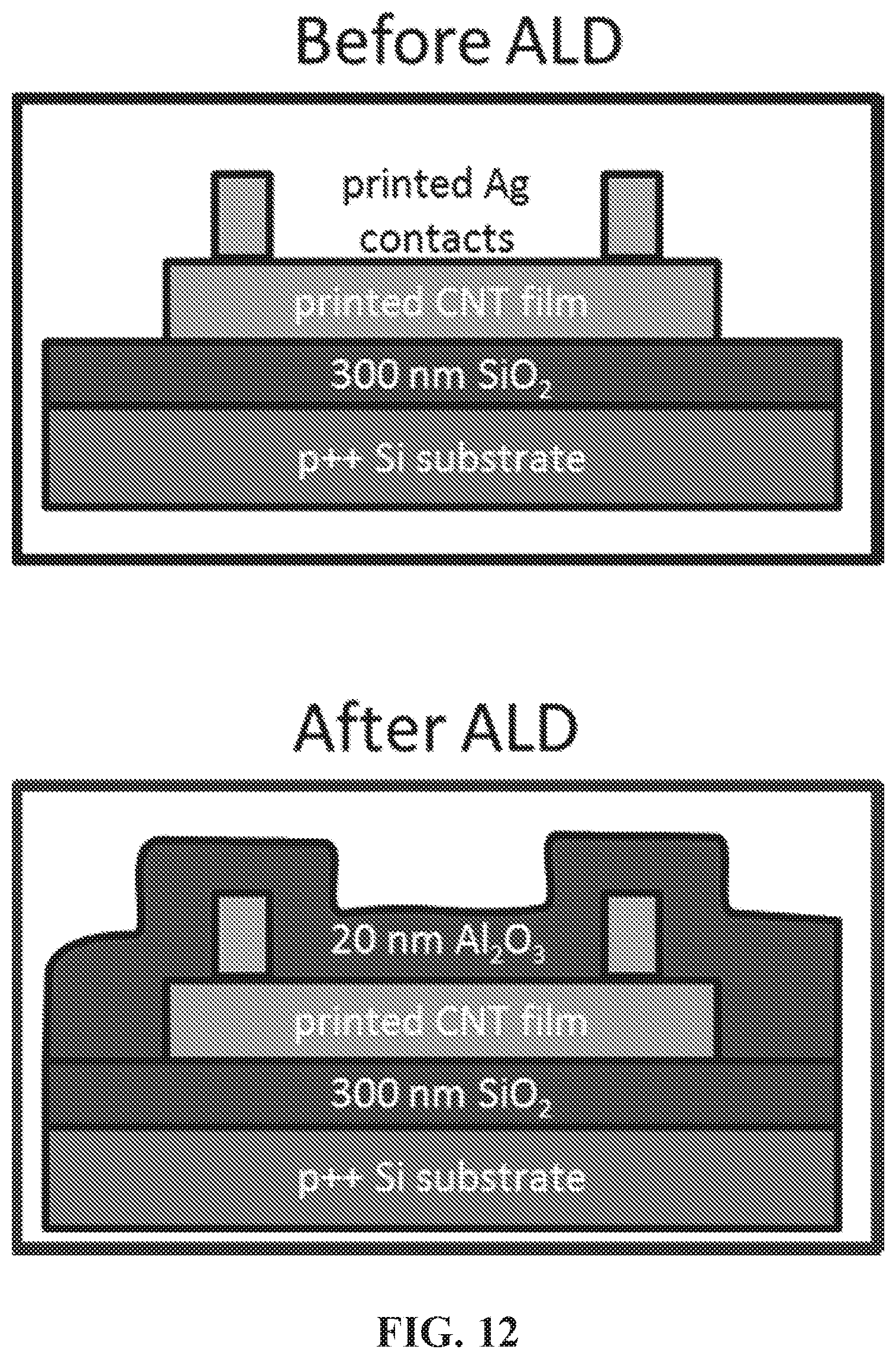
D00019

D00020

D00021

D00022

D00023

D00024

D00025

D00026

D00027

D00028

D00029

D00030

D00031

D00032

D00033

D00034

D00035

D00036

D00037

D00038

D00039

D00040

D00041

D00042


XML
uspto.report is an independent third-party trademark research tool that is not affiliated, endorsed, or sponsored by the United States Patent and Trademark Office (USPTO) or any other governmental organization. The information provided by uspto.report is based on publicly available data at the time of writing and is intended for informational purposes only.
While we strive to provide accurate and up-to-date information, we do not guarantee the accuracy, completeness, reliability, or suitability of the information displayed on this site. The use of this site is at your own risk. Any reliance you place on such information is therefore strictly at your own risk.
All official trademark data, including owner information, should be verified by visiting the official USPTO website at www.uspto.gov. This site is not intended to replace professional legal advice and should not be used as a substitute for consulting with a legal professional who is knowledgeable about trademark law.