Wide Switching Frequency Range Switched Mode Power Supply Control Topology
XIE; Jianzhang ; et al.
U.S. patent application number 16/794110 was filed with the patent office on 2020-11-26 for wide switching frequency range switched mode power supply control topology. The applicant listed for this patent is TEXAS INSTRUMENTS INCORPORATED. Invention is credited to Yue WU, Jianzhang XIE, Yihan YAO, Wei ZHAO.
| Application Number | 20200373841 16/794110 |
| Document ID | / |
| Family ID | 1000004671303 |
| Filed Date | 2020-11-26 |


View All Diagrams
| United States Patent Application | 20200373841 |
| Kind Code | A1 |
| XIE; Jianzhang ; et al. | November 26, 2020 |
WIDE SWITCHING FREQUENCY RANGE SWITCHED MODE POWER SUPPLY CONTROL TOPOLOGY
Abstract
Aspects of the disclosure provide for a circuit. In some examples, the circuit includes a timing circuit and a state machine circuit. The timing circuit determines a relationship between a duty cycle of a power converter and a threshold value. The state machine circuit is coupled to the timing circuit and includes a plurality of states including a buck state, a boost state, and a buck-boost state. The state machine circuit transitions among the plurality of states according to time domain control and voltage domain control, based at least partially on the determined relationship between the duty cycle and the threshold value, transitions among the states according to the time domain control when the time domain control indicates an exit from the buck-boost state, and transitions among the states according to the voltage domain control when the voltage domain control indicates the exit from a buck-boost state.
| Inventors: | XIE; Jianzhang; (Shanghai, CN) ; ZHAO; Wei; (Shanghai, CN) ; YAO; Yihan; (Shanghai, CN) ; WU; Yue; (Shanghai, CN) | ||||||||||
| Applicant: |
|
||||||||||
|---|---|---|---|---|---|---|---|---|---|---|---|
| Family ID: | 1000004671303 | ||||||||||
| Appl. No.: | 16/794110 | ||||||||||
| Filed: | February 18, 2020 |
Related U.S. Patent Documents
| Application Number | Filing Date | Patent Number | ||
|---|---|---|---|---|
| 62850775 | May 21, 2019 | |||
| Current U.S. Class: | 1/1 |
| Current CPC Class: | H02M 3/1582 20130101 |
| International Class: | H02M 3/158 20060101 H02M003/158 |
Claims
1. A circuit, comprising: a timing circuit configured to determine a relationship between a duty cycle of a power converter and a threshold value; and a state machine circuit coupled to the timing circuit and comprising a plurality of states including a buck state, a boost state, and a buck-boost state, wherein the state machine circuit is configured to: transition among the plurality of states according to time domain control and voltage domain control, based at least partially on the determined relationship between the duty cycle of the power converter and the threshold value; transition among the plurality of states according to the time domain control when the time domain control indicates an exit from the buck-boost state; and transition among the plurality of states according to the voltage domain control when the voltage domain control indicates the exit from a buck-boost state.
2. The circuit of claim 1, wherein the buck state is configured to: generate a control signal for controlling the power converter in a buck mode of operation; transition to a boost state of the plurality of states when a ratio of an input voltage (VIN) to an output voltage (VOUT) is less than a maximum VIN to VOUT ratio regulatable by the power converter in a boost mode of operation; and transition to a buck-boost state of the plurality of states when an off-time of the buck mode of operation is less than or equal to a minimum off-time for the power converter while operating in the buck mode of operation and the VIN to VOUT ratio is greater than or equal to the maximum VIN to VOUT ratio regulatable by the power converter in the boost mode of operation.
3. The circuit of claim 1, wherein the boost state is configured to: generate a control signal for controlling the power converter in a boost mode of operation; transition to a buck state of the plurality of states when a ratio of an input voltage (VIN) to an output voltage (VOUT) is greater than a minimum VIN to VOUT ratio regulatable by the power converter in a buck mode of operation; and transition to a buck-boost state of the plurality of states when an on-time of the boost mode of operation is less than or equal to a minimum on-time for the power converter while operating in the boost mode of operation and the VIN to VOUT ratio is less than or equal to the minimum VIN to VOUT ratio regulatable by the power converter in the buck mode of operation.
4. The circuit of claim 1, wherein the buck-boost state is configured to: generate a control signal for controlling the power converter in a buck-boost mode of operation; and transition to a buck state of the plurality of states when: an off-time of a buck cycle of the buck-boost mode of operation is greater than or equal to a hysteresis off-time and an on-time of a boost cycle of the buck-boost mode of operation is less than or equal to a minimum on-time for the power converter while operating in a boost mode of operation; or an input voltage (VIN) to an output voltage (VOUT) is greater than a minimum VIN to VOUT ratio regulatable by the power converter in a buck mode of operation.
5. The circuit of claim 1, wherein the buck-boost state is configured to: generate a control signal for controlling the power converter in a buck-boost mode of operation; and transition to a boost state of the plurality of states when: an on-time of a boost cycle of the buck-boost mode of operation is greater than or equal to a hysteresis on-time and an off-time of a buck cycle of the buck-boost mode of operation is less than or equal to a minimum off-time for the power converter while operating in the buck mode of operation; or an input voltage (VIN) to an output voltage (VOUT) ratio is less than a maximum VIN to VOUT ratio regulatable by the power converter in a boost mode of operation.
6. The circuit of claim 1, wherein the time domain control is configured to control operation of the state machine when the power converter is operating at a frequency less than about 500 kilohertz.
7. The circuit of claim 1, wherein the voltage domain control is configured to control operation of the state machine when the power converter is operating at a frequency greater than about 1.8 megahertz.
8. The circuit of claim 1, wherein the timing circuit is further configured to: receive a first clock signal defining a first threshold value; receive a second clock signal defining a second threshold value; receive a signal indicating the duty cycle of the power converter; determine a relationship of the signal indicating the duty cycle of the power converter to the first threshold value and the second threshold value; output a first signal indicating the relationship of the signal indicating the duty cycle of the power converter to the first threshold value; and output a second signal indicating the relationship of the signal indicating the duty cycle of the power converter to the second threshold value.
9. The circuit of claim 1, further comprising a first comparator that comprises: a first input terminal configured to receive a signal representative of an output voltage (VOUT) of the power converter multiplied by a maximum input voltage (VIN) to VOUT ratio regulatable by the power converter in a boost mode of operation; a second input terminal configured to receive VIN; and an output terminal coupled to an input terminal of the state machine circuit and configured to output a signal indicating whether a VIN to VOUT ratio of the power converter is less than the maximum VIN to VOUT ratio regulatable by the power converter in the boost mode of operation.
10. The circuit of claim 1, further comprising a second comparator that comprises: a first input terminal configured to receive a signal representative of an input voltage (VIN) of the power converter divided by a minimum VIN to output voltage (VOUT) ratio regulatable by the power converter in a buck mode of operation; a second input terminal configured to receive VOUT; and an output terminal coupled to an input terminal of the state machine circuit and configured to output a signal indicating whether a VIN to VOUT ratio of the power converter is greater than the minimum VIN to VOUT ratio regulatable by the power converter in a boost mode of operation.
11. A circuit, comprising: a timing circuit configured to determine a relationship between a duty cycle of a power converter and a threshold value; and a state machine circuit coupled to the timing circuit and comprising a plurality of states including a buck-boost state and at least another state, wherein the state machine circuit is configured to: transition from the another state to the buck-boost state, based at least partially on the determined relationship between the duty cycle of the power converter and the threshold value, when both time domain control and voltage domain control indicate an entry to the buck-boost state; and transition from the buck-boost state to the another state, based at least partially on the determined relationship between the duty cycle of the power converter and the threshold value, when the time domain control or the voltage domain control indicates an exit from the buck-boost state.
12. The circuit of claim 11, wherein the another state is a buck state, and wherein the state machine circuit is configured to, while operating in the buck-boost state, transition from the buck-boost state to the buck state when: an off-time of a buck cycle of the power converter is greater than or equal to a hysteresis off-time and an on-time of a boost cycle of the power converter is less than or equal to a minimum on-time for a boost cycle of the power converter; or an input voltage (VIN) to an output voltage (VOUT) is greater than a minimum VIN to VOUT ratio regulatable by the power converter in a buck mode of operation.
13. The circuit of claim 11, wherein the another state is a boost state, and wherein the state machine circuit is configured to, while operating in the buck-boost state, transition from the buck-boost state to the boost state when: an on-time of a boost cycle of the power converter is greater than or equal to a hysteresis on-time and an off-time of a buck cycle of the power converter is less than or equal to a minimum off-time for a buck cycle of the power converter; or an input voltage (VIN) to an output voltage (VOUT) is less than a maximum VIN to VOUT ratio regulatable by the power converter in a boost mode of operation.
14. The circuit of claim 11, wherein the time domain control dominates control of the state machine and the power converter when a switching frequency of the power converter is less than about 500 kilohertz, and wherein the voltage domain control dominates control of the state machine and the power converter when the switching frequency of the power converter is greater than about 1.8 megahertz.
15. The circuit of claim 11, wherein an amount of time in which the state machine remains in the buck-boost state when controlled by both the time domain control and the voltage domain control is reduced when compared to another state machine controlled by only the time domain control or the voltage domain control.
16. A system, comprising: a load; a power converter coupled to the load and configured to provide the load with an output voltage (VOUT) switched from an input voltage (VIN) by the power converter; a controller coupled to the power converter and configured to control the power converter to switch VIN to VOUT by: generating a plurality of clock signals; determine a relationship between a duty cycle of the power converter and a threshold value determined according to at least some of the plurality of clock signals; and control the power converter to operate in a buck-boost mode of operation based at least partially on the determined relationship between the duty cycle of the power converter and the threshold value when both time domain control and voltage domain control specify operation of the power converter in the buck-boost mode of operation.
17. The system of claim 16, wherein the controller comprises a timing circuit configured to: receive a first clock signal defining a first threshold value; receive a second clock signal defining a second threshold value; receive a signal indicating the duty cycle of the power converter; determine a relationship of the signal indicating the duty cycle of the power converter to the first threshold value and the second threshold value; output a first signal indicating the relationship of the signal indicating the duty cycle of the power converter to the first threshold value; and output a second signal indicating the relationship of the signal indicating the duty cycle of the power converter to the second threshold value.
18. The system of claim 16, wherein the controller comprises a state machine circuit configured to: transition to a buck-boost state, based at least partially on the determined relationship between the duty cycle of the power converter and the threshold value, when both time domain control and voltage domain control indicate an entry to the buck-boost state; and transition from the buck-boost state, based at least partially on the determined relationship between the duty cycle of the power converter and the threshold value, when the time domain control or the voltage domain control indicates an exit from the buck-boost state.
19. The system of claim 16, wherein the controller comprises a state machine circuit configured to: transition to a buck-boost state when an off-time of a buck mode of operation of the power converter is less than or equal to a minimum off-time for the power converter while operating in the buck mode of operation and an input voltage (VIN) to an output voltage (VOUT) ratio is greater than or equal to the maximum VIN to VOUT ratio regulatable by the power converter in a boost mode of operation; or transition to the buck-boost state when an on-time of the boost mode of operation is less than or equal to a minimum on-time for the power converter while operating in the boost mode of operation and the VIN to VOUT ratio is less than or equal to the minimum VIN to VOUT ratio regulatable by the power converter in the buck mode of operation.
20. The system of claim 16, wherein the controller comprises a state machine circuit configured to: transition to a buck state when: an off-time of a buck cycle of the buck-boost mode of operation is greater than or equal to a hysteresis off-time and an on-time of a boost cycle of the buck-boost mode of operation is less than or equal to a minimum on-time for the power converter while operating in a boost mode of operation; or an input voltage (VIN) to an output voltage (VOUT) is greater than a minimum VIN to VOUT ratio regulatable by the power converter in a buck mode of operation; or transition to a boost state when: an on-time of a boost cycle of the buck-boost mode of operation is greater than or equal to a hysteresis on-time and an off-time of a buck cycle of the buck-boost mode of operation is less than or equal to a minimum off-time for the power converter while operating in the buck mode of operation; or the VIN to VOUT ratio less than a maximum VIN to VOUT ratio regulatable by the power converter in a boost mode of operation.
21. The system of claim 16, wherein the time domain control dominates control of a state machine implemented by the controller and the power converter when a switching frequency of the power converter is less than about 500 kilohertz, and wherein the voltage domain control dominates control of the state machine and the power converter when the switching frequency of the power converter is greater than about 1.8 megahertz.
Description
CROSS-REFERENCE TO RELATED APPLICATIONS
[0001] The present application claims priority to U.S. Provisional Patent Application No. 62/850,775, which was filed May 21, 2019, is titled "Buck-Boost DC-DC Converter with Wide Switching Frequency Range," and is hereby incorporated herein by reference in its entirety.
BACKGROUND
[0002] A switched mode power supply (SMPS) transfers power from an input power source to a load by switching one or more power transistors coupled through a switch node/terminal to an energy storage element (such as an inductor/transformer and/or capacitor), which is capable of coupling to the load. The power transistors can be included in a power converter that includes, or is capable of coupling to, the energy storage element. An SMPS can include an SMPS controller to provide one or more gate drive signals to the power transistor(s). Varying switching frequencies are applicable to certain application environments for the SMPS, but optimizing an SMPS controller for a wide range of switching frequencies can bring challenges.
SUMMARY
[0003] Aspects of the disclosure provide for a circuit. In at least some examples, the circuit includes a timing circuit and a state machine circuit. The timing circuit is configured to determine a relationship between a duty cycle of a power converter and a threshold value. The state machine circuit is coupled to the timing circuit and includes a plurality of states including a buck state, a boost state, and a buck-boost state. The state machine circuit is configured to transition among the plurality of states according to time domain control and voltage domain control, based at least partially on the determined relationship between the duty cycle of the power converter and the threshold value, transition among the plurality of states according to the time domain control when the time domain control indicates an exit from the buck-boost state, and transition among the plurality of states according to the voltage domain control when the voltage domain control indicates the exit from a buck-boost state.
[0004] Other aspects of the disclosure provide for a circuit. In at least some examples, the circuit includes a timing circuit and a state machine circuit. The timing circuit is configured to determine a relationship between a duty cycle of a power converter and a threshold value. The state machine circuit is coupled to the timing circuit and comprising a plurality of states including a buck-boost state and at least another state. The state machine circuit is configured to transition from the another state to the buck-boost state, based at least partially on the determined relationship between the duty cycle of the power converter and the threshold value, when both time domain control and voltage domain control indicate an entry to the buck-boost state. The state machine circuit is further configured to transition from the buck-boost state to the another state, based at least partially on the determined relationship between the duty cycle of the power converter and the threshold value, when the time domain control or the voltage domain control indicates an exit from the buck-boost state.
[0005] Other aspects of the disclosure provide for a system. In at least some examples, the system includes a load, a power converter, and a controller. The power converter is coupled to the load and configured to provide the load with an output voltage (VOUT) switched from an input voltage (VIN) by the power converter. The controller is coupled to the power converter and configured to control the power converter to switch VIN to VOUT. The controller switches VIN to VOUT by generating a plurality of clock signals, determining a relationship between a duty cycle of the power converter and a threshold value determined according to at least some of the plurality of clock signals, and controlling the power converter to operate in a buck-boost mode of operation based at least partially on the determined relationship between the duty cycle of the power converter and the threshold value when both time domain control and voltage domain control specify operation of the power converter in the buck-boost mode of operation.
BRIEF DESCRIPTION OF THE DRAWINGS
[0006] For a detailed description of various examples, reference will now be made to the accompanying drawings in which:
[0007] FIG. 1 shows a block diagram of an illustrative SMPS in accordance with various examples;
[0008] FIG. 2 shows a schematic diagram of an illustrative buck-boost power converter in accordance with various examples;
[0009] FIG. 3 shows a schematic diagram of an illustrative mode transition control circuit in accordance with various examples;
[0010] FIG. 4 shows an illustrative state diagram in accordance with various examples;
[0011] FIG. 5 shows an illustrative graph of buck-boost region width versus switching frequency in accordance with various examples;
[0012] FIG. 6 shows a schematic diagram of an illustrative timing detection circuit in accordance with various examples;
[0013] FIG. 7 shows an illustrative timing diagram in accordance with various examples;
[0014] FIG. 8 shows an illustrative timing diagram in accordance with various examples;
[0015] FIG. 9 shows an illustrative timing diagram in accordance with various examples;
[0016] FIG. 10 shows an illustrative timing diagram in accordance with various examples; and
[0017] FIG. 11 shows an illustrative timing diagram in accordance with various examples.
DETAILED DESCRIPTION
[0018] In some architectures (such as buck-boost), a switched mode power supply (SMPS) includes, or is capable of coupling to, an output/bulk capacitor in parallel with the load. A SMPS controller switches the power transistor(s) to form circuit arrangements with energy storage element(s) to supply a load current to the load and/or to the output/bulk capacitor to maintain a regulated output voltage (e.g., by filtering the switched load current). For example, a power transistor can be coupled through the switch node/terminal to an energy storage inductor. The energy storage inductor is switched by the SMPS controller between charge and discharge cycles to supply inductor current (e.g., current through the energy storage inductor) to the load and to the output/bulk capacitor to filter the inductor current to maintain the regulated output voltage. In some examples, an SMPS can be configured for operation as a constant current source with an energy storage element but with no output/bulk capacitor.
[0019] The power transistors can be implemented as metal oxide semiconductor field effect transistors (MOSFETs) or any other suitable solid-state transistor devices (e.g., such as bi-polar junction transistors (BJTs)). As an input voltage (VIN), or an output voltage (VOUT), of the power converter varies, the SMPS controller may control the power converter to operate in different modes of operation. For example, when VIN is greater than VOUT, the SMPS controller may control the power converter to operate in a buck mode of operation. When VIN is less than VOUT, the SMPS controller may control the power converter to operate in a boost mode of operation. When VIN is approximately equal to VOUT, the SMPS controller may control the power converter to operate in a buck-boost mode of operation. In at least some examples, minimizing an amount of time that the power converter operates in the buck-boost mode of operation may be advantageous. For example, when operating in the buck-boost mode of operation, output ripple of the power converter as present in VOUT or an inductor current of the power converter, is greater than when operating in the buck or boost mode of operation. In at least some implementations, the ripple in the buck-boost mode of operation is approximately double the ripple during the buck or boost mode of operation. For at least some buck-boost power converter implementations it is advantageous to minimize ripple, for example, to reduce a need for, or strength of, filtering of VOUT generated and output by the buck-boost power converter.
[0020] To control a mode of operation of the power converter, the SMPS controller provides gate control signals to one or more power transistors of the power converter. A value of each of these gate control signals determines whether a respective power transistor receiving the gate control signal is in a conductive state (e.g., turned on) or in a non-conductive state (e.g., turned off). To change a mode of operation of the power converter, the SMPS controller modifies a value of one or more of the gate control signals to turn one or more of the power transistors on or off. Additionally, while remaining in a mode of operation of the power converter, the SMPS controller may modify a value of one or more of the gate control signals, for example, to alternatively turn on and turn off one or more power transistors.
[0021] Generally, the SMPS controller controls the power converter to operate at a particular frequency. Some frequencies, such as high frequencies (e.g., greater than about 1.8 megahertz (MHz)), enable a smaller physical footprint of the power converter and/or SMPS controller by enabling the use of smaller circuit components. Other frequencies, such as low frequencies (e.g., less than about 500 kilohertz (kHz)), enable increased efficiency of a power converter by reducing switching losses of the power converter. Often, the SMPS controller implements a fixed-frequency control scheme that is optimized for either high frequency operation or low frequency operation. However, an SMPS controller optimized for operation across a wide frequency range may be advantageous in providing increased flexibility in implementing the SMPS controller.
[0022] At least some aspects of the present disclosure relate to a controller suitable for controlling a power converter, such as in a SMPS. In at least one example, the controller includes elements suitable for implementing a dual hysteresis control scheme. The dual hysteresis control scheme, in at least some examples, is dominated by one type of control when the power converter is operating at low frequencies (e.g., less than about 1.2 MHz, less than about 500 kHz, etc.) and is dominated by another type of control when the power converter is operating at high frequencies (e.g., greater than about 1.2 MHz, greater than about 1.8 MHz, etc.). For example, the dual hysteresis control scheme is dominated by time domain hysteresis control when the power converter is operating at low frequencies and is dominated by voltage domain hysteresis control when the power converter is operating at high frequencies.
[0023] The controller controls the power converter to operate in a mode of operation according to the dual hysteresis control scheme. For example, the controller controls the power converter to operate in a mode of operation based on a minimum of buck-boost regions determined by the time domain hysteresis control and the voltage domain hysteresis control. For example, if the buck-boost region of operation is defined according to a ratio of VOUT to VIN, a value of the buck-boost region under control of the dual hysteresis control scheme is minimized when compared to a value of the buck-boost region under individual control of the time domain hysteresis control or the voltage domain hysteresis control. In at least some examples, implementing the dual hysteresis control of the present disclosure provides a minimized duration of operation in the buck-boost mode and a minimum achievable inductor current ripple in buck-boost mode over a wide range of switching frequencies (e.g., such as about 200 kHz to about 2 MHz). For example, for a power converter inductor having an inductance of about 4 microhenries (uH) operating at a switching frequency of about 400 kHZ and VOUT of about 10 volts (V), the dual hysteresis control of the present disclosure limits inductor current ripple to about 1.5 amps (A) while the power converter is in the buck-boost mode of operation.
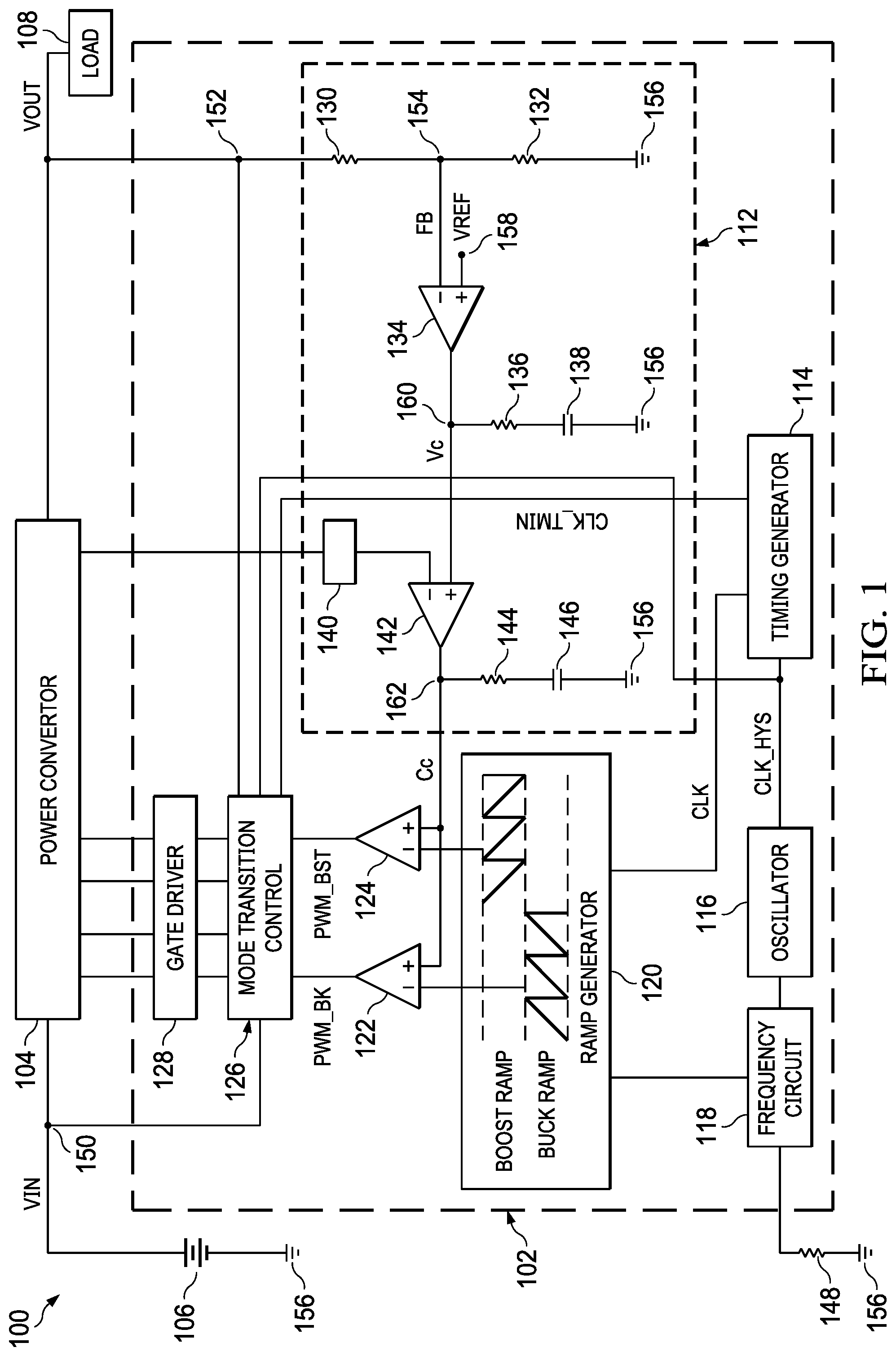
[0024] Turning now to FIG. 1, a block diagram of an illustrative SMPS 100 is shown. In at least one example, the SMPS 100 includes a controller 102 and a power converter 104. The SMPS 100, at least through the power converter 104, switches power from a node 150, provided by a power source 106, to a load 108. The power converter 104 is, for example, a buck-boost power converter that is capable of operating according to a buck mode of operation, a boost mode of operation, and a buck-boost mode of operation. In at least one example, the controller 102 includes, or is configured to couple to, a feedback circuit 112, a timing generator 114, an oscillator 116, a frequency circuit 118, a ramp generator 120, a comparator 122, a comparator 124, mode transition control circuit 126, and a gate driver 128. For the sake of description, the SMPS 100 is illustrated and described as implementing average current mode control over the power converter 104. However, the dual hysteresis control scheme of the present disclosure is equally applicable to other control methods, such as peak current mode control, voltage mode control, or any other suitable form of control implemented in a fixed frequency system.
[0025] At least one example of the SMPS 100 includes at least some aspects of the controller 102 and the power converter 104 on a same semiconductor die and/or in a same component package, while in other examples the controller 102 and the power converter 104 may be fabricated separately and configured to couple together. For example, at least some aspects of the controller 102 may be fabricated separately and coupled together. Accordingly, while illustrated as including the gate driver 128, in at least one example the controller 102 does not include the gate driver 128 and instead is configured to couple to the gate driver 128. Similarly, other components illustrated as being included in the controller 102 may instead be configured to couple, in whole or in part, to the controller 102 and not be included on a same semiconductor die and/or in a same component package as the controller 102.
[0026] In at least one example, the feedback circuit 112 includes a resistor 130 coupled between a node 152 and a node 154 and a resistor 132 coupled between the node 154 and a ground node 156. The feedback circuit 112 further includes an amplifier 134 having a first input terminal (e.g., a non-inverting input terminal) coupled to a node 158 and configured to receive a reference voltage (VREF) at the node 158. The amplifier 134 further has a second input terminal (e.g., an inverting input terminal) coupled to the node 154, and an output terminal coupled to a node 160. A feedback signal (FB) is present at the node 154 and is a scaled representation of VOUT, scaled according to a ratio of resistance of the resistor 132 to resistance of the resistor 130. A signal (VC) is present at the node 160, output by the amplifier 134 based on a difference between VREF and FB. A resistor 136 is coupled between the node 160 and a top plate of a capacitor 138 and a bottom plate of the capacitor 138 is coupled to the ground node 156. The feedback circuit 112 further includes a current sense circuit 140 and an amplifier 142. The current sense circuit 140 is configured to couple to the power converter 104 to generate an output signal (VI) that is a voltage representation of a current flowing through the power converter 104. The amplifier 142 has a first input terminal (e.g., a positive or non-inverting input terminal) coupled to the node 160, a second input terminal (e.g., a negative or inverting input terminal) coupled to an output terminal of the current sense circuit 140, and an output terminal coupled to a node 162. A current control signal (CC) is present at the node 162, output by the amplifier 142 based on a difference between VC and VI. A resistor 144 is coupled between the node 162 and a top plate of a capacitor 146 and a bottom plate of the capacitor 146 is coupled to the ground node 156.
[0027] The timing generator 114, in at least some examples, has a first output terminal coupled to the oscillator 116 and the mode transition control circuit 126, a second output terminal coupled to the ramp generator 120, and a third output terminal coupled to the mode transition control circuit 126. In at least some examples, the timing generator 114 includes any one or more components suitable for generating additional clock signals based on a received clock signal. For example, the timing generator 114 includes one or more delay cells (not shown) configured to implement a fixed or variable delay in a received clock signal to generate an additional clock signal. In at least one example, the timing generator 114 receives CLK_HYS from the oscillator 116, generates and outputs CLK to the ramp generator 120, and generates and outputs CLK_TMIN to the mode transition control circuit 126.
[0028] The oscillator 116, in at least some examples, is any component suitable for generating a clock signal, illustrated in FIG. 1 as CLK_HYS. A frequency of CLK_HYS is determined, in at least some examples, based on a value of a signal received from the frequency circuit 118. For example, the frequency circuit 118 generates a current signal ICLK based at least partially on a value of a resistor 148 coupled to the frequency circuit 118. The frequency circuit 118 outputs ICLK to the oscillator 116 to enable the oscillator 116 to generate CLK_HYS at least partially according to ICLK. In at least some examples, the frequency circuit 118 further outputs ICLK to the ramp generator 120.
[0029] The ramp generator 120, in at least some examples, is any component or components suitable for generating buck and boost ramp signals for use in controlling the power converter 104. In at least some examples, the buck and boost ramp signals are generated by charging and resetting (e.g., discharging) one or more capacitors (not shown) at a specified rate of charge, specified by a current value of a signal charging the one or more capacitors. In at least some examples, based on the received CLK and ICLK signals, the ramp generator 120 generates and outputs the buck ramp signal and the boost ramp signal.
[0030] The comparator 122 includes a first input terminal (e.g., a positive or non-inverting input terminal) coupled to the node 162, a second input terminal (e.g., a negative or inverting input terminal) coupled to the ramp generator 120 and configured to receive the buck ramp signal from the ramp generator 120, and an output terminal. The comparator 124 includes a first input terminal (e.g., a positive or non-inverting input terminal) coupled to the node 162, a second input terminal (e.g., a negative or inverting input terminal) coupled to the ramp generator 120 and configured to receive the boost ramp signal from the ramp generator 120, and an output terminal. In at least some examples, a control signal PWM_BK is present at the output terminal of the comparator 122 and a control signal PWM_BST is present at the output terminal of the comparator 124. In some examples, PWM_BK has an asserted value when CC is greater in value that the buck ramp and a de-asserted value when CC is less in value than the buck ramp. Similarly, in some examples PWM_BST has an asserted value when CC is greater in value than the boost ramp and a de-asserted value when CC is less in value than the boost ramp.
[0031] The mode transition control circuit 126 has a plurality of input terminals configured to receive at least CLK_TMIN, CLK_HYS, PWM_BK, PWM_BST, VOUT, and VIN (collectively referred to with respect to the mode transition control circuit 126 as the received signals). In at least some examples, the mode transition control circuit 126 includes or implements a state machine to generate one or more control signals for controlling the power converter 104 according to the received signals. Operation of the mode transition control circuit 126 is discussed in greater detail below.
[0032] In at least one example, the SMPS 100 is configured to receive VIN from the power source 106 at the node 150 and provide VOUT at the node 152 for supplying the load 108. VOUT is based at least partially on VIN and VREF as received by the SMPS 100 at the node 158. VREF may be received from any suitable device (not shown) such as a processor, microcontroller, or any other device exerting control over the SMPS 100 to control a value of VOUT. In at least one example, VREF has a value representative of a desired (e.g., user-desired, target, preconfigured, programmed, etc.) value of FB. Accordingly, in at least some implementations, the controller 102 receives one or more signals from the power converter 104. For example, the controller 102 may receive VOUT from the power converter 104 and/or an inductor current (IL) of the power converter 104. In various examples, IL may be a value directly measured from an inductor (not shown) of the power converter 104 (or a terminal of another component of the power converter 104 to which the inductor is also coupled) or a value sensed from a sense element (not shown) of the power converter 104. The sense element is, for example, a sense resistor, a transistor, or any other component or combination of components capable of measuring IL of the power converter 104 and providing the value representative of IL to the controller 102. In at least one example, the value representative of IL is provided to the feedback circuit 112 for generation of VI and VOUT is provided to the feedback circuit 112 and the mode transition control circuit 126.
[0033] In at least one example, the feedback circuit 112 is configured to receive VREF and VOUT and generate VC indicating a variation in VREF from VFB. VC is referred to in some examples as an error signal. In at least some examples, FB is an output of a voltage divider formed of the resistor 130 and the resistor 132, where an input to the voltage divider is VOUT. VC is subsequently filtered by the resistor 136 and the capacitor 138 before being received by the amplifier 142. The amplifier 142, in at least one example, is configured to receive VC and VI and generate CC indicating a variation in VC from VI. CC is subsequently filtered by the resistor 144 and the capacitor 146 before being received by the comparator 122 and the comparator 124.
[0034] As discussed above, in at least one example the frequency circuit 118 generates and outputs a signal ICLK based on a resistance of the resistor 148. ICLK at least partially determines a frequency of a clock signal CLK_HYS generated and output by the oscillator 116. The timing generator 114 receives CLK_HYS and generates one or more additional clock signals (illustrated in FIG. 1 as CLK and CLK_TMIN) by manipulating CLK_HYS. For example, in at least one implementation, the timing generator 114 modifies CLK_HYS to generate CLK and CLK_TMIN by delaying CLK_HYS for one or more predetermined periods of time. In at least one example, the timing generator 114 generates CLK by delaying CLK_HYS according to a delay t.sub.hys (e.g., such that CLK=CLK_HYS+t.sub.hys) and generates CLK_TMIN according to a delay of t.sub.hys minus t.sub.min (e.g., such that CLK_TMIN=CLK_HYS+t.sub.hys-t.sub.min). The delay t.sub.hys, in at least some examples, is approximately equal to a hysteresis time for an on time (Ton_hys) of the power converter 104 when operating in the buck mode of operation and a hysteresis time for an off time (Toff_hys) of the power converter 104 when operating in the boost mode of operation. Further, the delay t.sub.min, in at least some examples, is approximately equal to a minimum on time (Ton_min) of the power converter 104 when operating in the boost mode of operation and an off time (Toff_min) of the power converter 104 when operating in the buck mode of operation. In at least one example, the timing generator 114 generates CLK and CLK_TMIN by implementing one or more delay cells of any suitable architecture. However, in at least one example, a series of digital circuit components implement the delay. For example, the delay is implemented by one or more d-flip flops, one or more digital inverter circuits, or any other circuit components suitable for implementing a delay, the scope of which is not limited herein.
[0035] The mode transition control circuit 126 receives CLK_TMIN, CLK_HYS, PWM_BK, PWM_BST, VOUT, and VIN and generates control signals for controlling the gate driver 128 to control the power converter 104. In at least one example, the mode transition control circuit 126 includes or otherwise implements a digital state machine to generate the control signals based on values of CLK_TMIN, CLK_HYS, PWM_BK, PWM_BST, VOUT, and/or VIN. To generate the control signals, in at least some examples, the mode transition control circuit 126 implements the dual hysteresis control scheme. In the dual hysteresis control scheme, at low frequencies of CLK_HYS the mode transition control circuit 126 generates the control signals according to time domain hysteresis control and generates the control signals according to voltage domain hysteresis control at high frequencies of CLK_HYS. Operation of the mode transition control circuit 126 will be discussed in greater detail below.
[0036] Based on the control signals received from the mode transition control circuit 126, the gate driver 128 generates gate control signals for controlling power transistors of the power converter 104, as discussed above. For example, the gate driver 128 generates gate control signals that alternatingly, and selectively, turn the power transistors of the power converter on and off to energize and de-energize elements such as an inductor and/or a capacitor (each not shown). This energizing and de-energizing provides the buck, boost, and/or buck-boost functionality discussed herein. The gate driver 128 is implemented according to any suitable architecture, the scope of which is not limited herein.
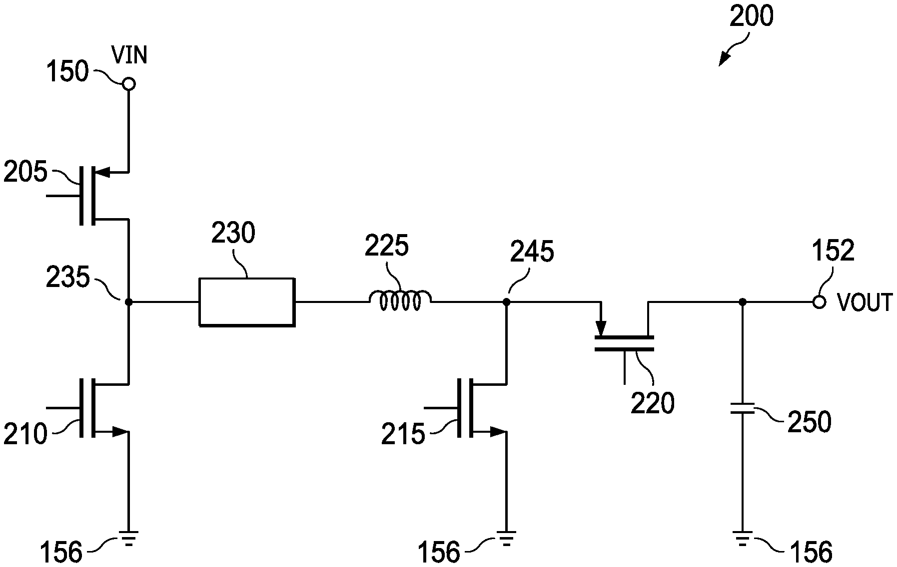
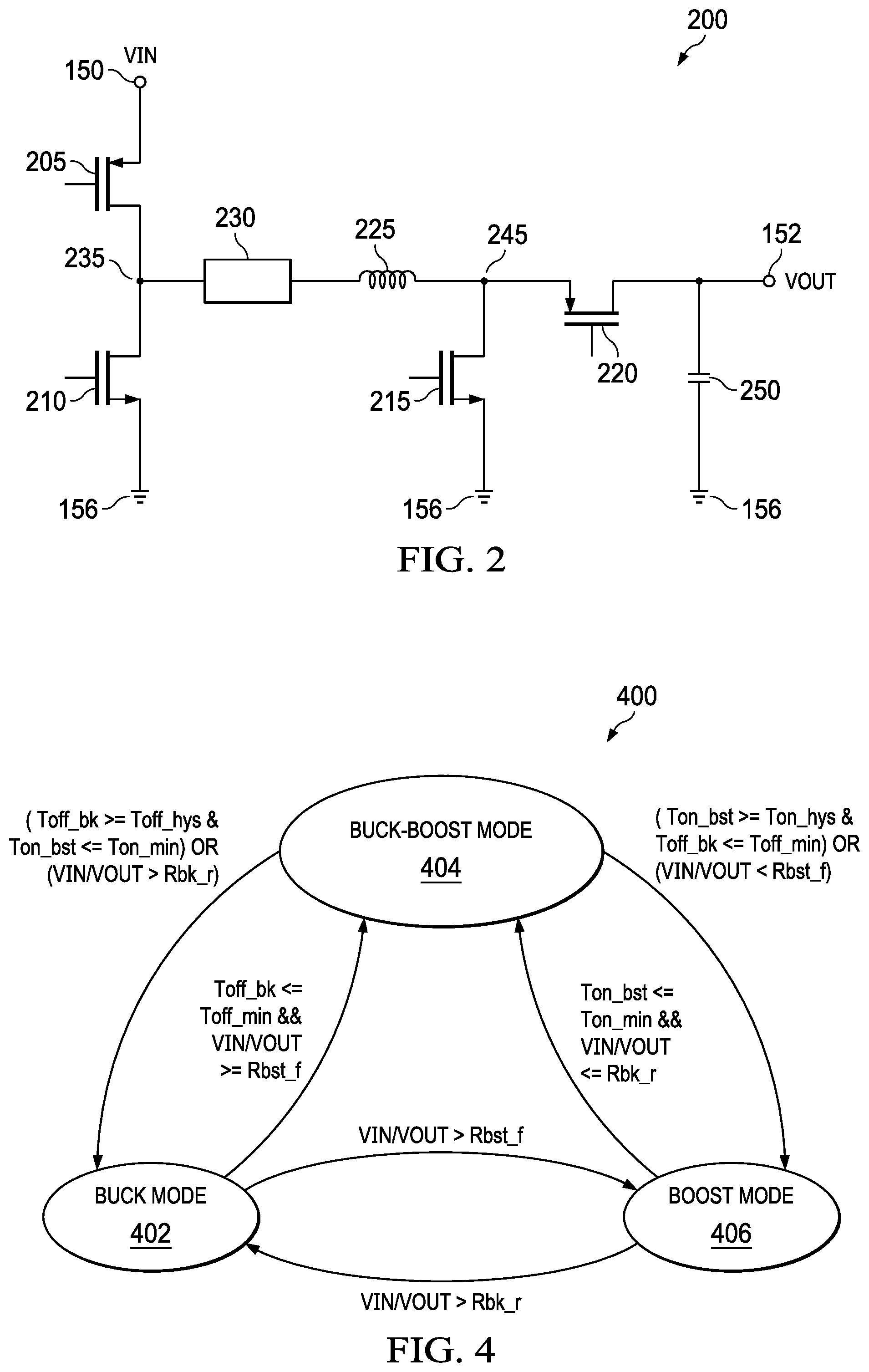
[0037] Turning now to FIG. 2, a schematic diagram of an illustrative buck-boost power converter 200 is shown. In at least one example, the buck-boost power converter 200 is suitable for implementation as the power converter 104 of the SMPS 100 of FIG. 1, discussed above. Accordingly, reference is made to at least some components or signals of FIG. 1 in describing FIG. 2.
[0038] In one example, the buck-boost power converter 200 includes a plurality of metal oxide semiconductor field effect transistors (MOSFETs) 205, 210, 215, and 220, and at least one energy storage device (illustrated in this example as an inductor 225). In another example, the buck-boost power converter 200 further includes a second inductor (not shown) and/or a fly-capacitor (not shown). In one example, the MOSFETs 205 and 220 are implemented as p-type MOSFETs (PMOS) and the MOSFETs 210 and 215 are implemented as n-type MOSFETs (NMOS). In at least one example, the buck-boost power converter 200 further includes a sense element 230 suitable for sensing IL of the inductor 225 and generating the signal representative of IL. The sense element 230 is, for example, a MOSFET, a resistor, or any other suitable circuit capable of, or having a means of, sensing, measuring, or detecting IL. In at least one example, the sense element 230 is implemented by one of the MOSFETs 205, 210, 215, or 220 such that the sense element 230 is not an independent, additional component of the buck-boost power converter 200. Further, in at least some examples, the sense element 230 also functions as, or as a component of, the current sense circuit 140.
[0039] In one example architecture, a source terminal of the MOSFET 205 is coupled to the node 150 and configured to receive VIN, a drain terminal of the MOSFET 205 is coupled to a node 235, and a gate terminal of the MOSFET 205 is coupled to a controller. The controller is, for example, the gate driver 128. A drain terminal of the MOSFET 210 is coupled to the node 235, a source terminal of the MOSFET 210 is coupled to the ground node 156, and a gate terminal of the MOSFET 210 is coupled to the controller. A first terminal of the inductor 225 is coupled to the node 235 and a second terminal of the inductor 225 is coupled to a node 245. In at least one example, the sense element 230 is coupled in series between node 235 and the first terminal of the inductor 225. A drain terminal of the MOSFET 215 is coupled to the node 245, a source terminal of the MOSFET 215 is coupled to the ground node 156, and a gate terminal of the MOSFET 215 is coupled to the controller. A source terminal of the MOSFET 220 is coupled to the node 245, a drain terminal of the MOSFET 220 is coupled to the node 152 at which VOUT is present, and a gate terminal of the MOSFET 220 is coupled to the controller. In at least one example, the inductor 225 is implemented as an external component such that the buck-boost power converter 200 does not include the inductor 225 but is configured to couple to the inductor 225 between the node 235 and the node 245. In at least one example, the buck-boost power converter 200 is configured to couple to a capacitor 250 (e.g., such as a filtering capacitor) between the drain terminal of the MOSFET 220 and the ground node 156.
[0040] In one example, the MOSFETs 205, 210, 215, and/or 220 are controlled to turn on (e.g., conduct current between their respective drain terminals and source terminals) and/or turn off (e.g., cease conducting current between their respective drain terminals and source terminals) based on a signal received at their respective gate terminals. For example, based on a gate control signal received from the controller (e.g., as output by the gate driver 128 under control of the mode transition control circuit 126), one or more of the MOSFETs 205, 210, 215, and/or 220 are controlled to turn on or turn off. The MOSFETs 205, 210, 215, and/or 220 may turn on (or off) based on a value, or relationship between values, present at one or more of their respective gate terminals and/or source terminals. Based on which of the MOSFETs 205, 210, 215, or 220 are turned on at a given time, which of the MOSFETs 205, 210, 215, or 220 are turned off at a given time, and a sequence of turning on and/or off the MOSFETs 205, 210, 215, and/or 220, the buck-boost power converter 200 operates in a buck mode of operation, a boost mode of operation, or a buck-boost mode of operation.
[0041] Turning now to FIG. 3, a schematic diagram of an illustrative implementation of the mode transition control circuit 126 is shown. Accordingly, the mode transition control circuit 126 as shown in FIG. 3 is suitable for implementation in at least some examples of the controller 102 of the SMPS 100 of FIG. 1. Therefore, reference may be made in describing FIG. 3 to at least some components and/or signals introduced and/or described above with respect to FIG. 1.
[0042] In at least one example, the mode transition control circuit 126 includes a timing detection circuit 302, a comparator 304, a comparator 306, and a state machine circuit 308. The timing detection circuit 302 is configured to receive PWM_BK, PWM_BST, CLK_HYS, and CLK_TMIN. Based on at least some of PWM_BK, PWM_BST, CLK_HYS, and/or CLK_TMIN, the timing detection circuit 302 makes a plurality of timing determinations and outputs a plurality of signals to the state machine circuit 308 indicating a result of a respective one of the timing determinations. For example, the timing detection circuit 302 performs one or more calculations to determine whether an on time of the boost mode of operation (Ton_bst) of the power converter 104 is greater than or equal to Ton_hys, and whether Ton_bst is less than or equal to Ton_min. The timing detection circuit 302 further performs one or more calculations to determine whether an off time of the buck mode of operation (Toff_bk) is greater than or equal to Toff_hys, and whether Toff_bk is less than or equal to Toff_min. In at least some examples, one or more signals indicating results of these determinations are output by the timing detection circuit 302 to the state machine circuit 308. In at least some examples, Ton_hys and Toff_hys are determined, respectively, according to the following equations (1) and (2) in which t.sub.min is the minimum turn on/off time that power converter 104 and gate driver 128 can achieve and .DELTA. is a hysteresis factor to prevent control of the power converter 104 from oscillating between modes of operation.
Ton_hys=3t.sub.min+.DELTA. (1)
Toff_hys=3t.sub.min+.DELTA. (2)
[0043] In at least some examples, a minimum VIN to VOUT ratio that the power converter 104 can regulate while in the buck mode of operation is defined as R.sub.bk. In at least one implementation of the SMPS 100, R.sub.bk is determined according to the following equation (3) in which k is a hysteresis factor to prevent control of the power converter 104 from oscillating between modes of operation and T.sub.min is a switch period of the power converter 104 when operating at its highest supported switching frequency.
R bk = ( 1 + k 1 ) ( 1 + Toff_min T min - Toff_min ) ( 3 ) ##EQU00001##
[0044] In at least some examples, a maximum VIN to VOUT ratio that the power converter 104 can regulate while in the boost mode of operation is defined as R.sub.bst. In at least one implementation of the SMPS 100, R.sub.bst is determined according to the following equation (4) in which k2 is a hysteresis factor to prevent control of the power converter 104 from oscillating between modes of operation.
R bst = ( 1 - k 2 ) ( 1 - Ton_min T min ) ( 4 ) ##EQU00002##
[0045] The comparator 304 is configured to receive a value approximately equal to VOUT*R.sub.bst at a first input terminal (e.g., a positive or non-inverting input terminal) and receive VIN at a second input terminal (e.g., a negative or inverting input terminal). While not shown in FIG. 3, in at least some examples the signal VOUT*R.sub.bst is generated by a voltage divider that receives VOUT. In other examples, VOUT*R.sub.bst is formed in any suitable manner and by any suitable components. An output terminal of the comparator 304 is coupled to an input terminal of the state machine circuit 308. A signal output by the comparator 304 is asserted, in at least some examples, when VIN/VOUT is less than R.sub.bst and is de-asserted when VIN/VOUT is greater than R.sub.bst. The comparator 306 is configured to receive a value approximately equal to VIN/R.sub.bk at a first input terminal (e.g., a positive or non-inverting input terminal) and receive VOUT at a second input terminal (e.g., a negative or inverting input terminal). While not shown in FIG. 3, in at least some examples, the signal VIN/R.sub.bk is generated by a voltage divider that receives VOUT. In other examples, VIN/R.sub.bk is formed in any suitable manner and by any suitable components. An output terminal of the comparator 306 is coupled to an input terminal of the state machine circuit 308. A signal output by the comparator 306 is asserted, in at least some examples, when VIN/VOUT is greater than R.sub.bk and is de-asserted when VIN/VOUT is less than R.sub.bk.
[0046] The state machine circuit 308, in at least some examples, receives a plurality of signals as discussed herein and implements a state machine to generate control signals for controlling the gate driver 128 to control the power converter 104. Turning for a moment to FIG. 4, an illustrative state diagram 400 is shown. In at least some examples, the state diagram 400 illustrates states and transition conditions for the state machine implemented by the state machine circuit 308 of the mode transition control circuit 126. Accordingly, reference may be made to components and/or signals of one or more other figures of the disclosure in describing the state diagram 400. Additionally, description of the state diagram 400 begins with the buck state 402, making an assumption that the power converter 104 is first controlled to operate in the buck mode of operation. However, when the power converter 104 is instead controlled to first operate in the boost mode of operation, a first state of the state diagram 400 that may be implemented may be the boost state 406.
[0047] At buck state 402, the state machine circuit 308 generates control signals for controlling the power converter 104 to operate in the buck mode of operation. While controlling the power converter 104 to operate in the buck mode of operation, the state machine circuit 308 monitors a plurality of received input signals to determine whether to transition to the buck-boost state 404 or the boost state 406. For example, when operating in the buck state 402 and the state machine circuit 308 determines based on the received input signals that VIN/VOUT is less than R.sub.bst, the state machine circuit 308 transitions to the boost state 406. Similarly, when operating in the buck state 402 and the state machine circuit 308 determines based on the received input signals that Toff_bk is less than or equal to Toff_min and VIN/VOUT is greater than or equal to R.sub.bst, the state machine circuit 308 transitions to the buck-boost state 404.
[0048] At buck-boost state 404, the state machine circuit 308 generates control signals for controlling the power converter 104 to operate in the buck-boost mode of operation. For example, the state machine circuit 308 generates control signals to cause the power converter 104 to alternatingly operate in the buck mode of operation and the boost mode of operation. For example, the control signals generated by the state machine circuit 308 cause the power converter 104 to execute a buck cycle of operation, followed by a boost cycle of operation, followed by another buck cycle of operation and continuing in this alternating manner for as long as the state machine circuit 308 operates at buck-boost state 404. While controlling the power converter 104 to operate in the buck-boost mode of operation, the state machine circuit 308 monitors the plurality of received input signals to determine whether to transition to the buck state 402 or the boost state 406. For example, when operating in the buck-boost state 404 and the state machine circuit 308 determines based on the received input signals that Toff_bk is greater than or equal to Toff_hys and Ton_bst is less than or equal to Ton_min, or that VIN/VOUT is greater than R.sub.bk, the state machine circuit 308 transitions back to the buck state 402. Similarly, when operating in the buck-boost state 404 and the state machine circuit 308 determines based on the received input signals that Ton_bst is greater than or equal to Ton_hys and Toff_bk is less than or equal to Toff_min, or that VIN/VOUT is less than R.sub.bst, the state machine circuit 308 transition to the boost state 406.
[0049] At boost state 406, the state machine circuit 308 generates control signals for controlling the power converter 104 to operate in the boost mode of operation. While controlling the power converter 104 to operate in the boost mode of operation, the state machine circuit 308 monitors the plurality of received input signals to determine whether to transition to the buck state 402 or the buck-boost state 404. For example, when operating in the boost state 406 and the state machine circuit 308 determines, based on the received input signals that VIN/VOUT is greater than R.sub.bk, the state machine circuit 308 transitions back to the buck state 402. Similarly, when operating in the boost state 406 and the state machine circuit 308 determines based on the received input signals that Ton_bst is less than or equal to Ton_min and VIN/VOUT is less than R.sub.bk, the state machine circuit 308 transitions back to the buck-boost state 404.
[0050] As illustrated by the state diagram 400, transitions to and from the buck-boost state 404 are controlled by time domain or voltage domain control. In this way, the state machine circuit 308 implements the dual hysteresis control scheme of the present disclosure to minimize an amount of time for which the state machine circuit 308 is operating in the buck-boost state 404. For example, by transitioning to the buck-boost state 404 only when both time domain and voltage domain requirements are met, and transitioning out of the buck-boost state 404 when either time domain or voltage domain requirements are met, the state machine circuit 308 minimizes an amount of time operating in the buck-boost state 404. In at least some examples, the control scheme implemented by the state machine circuit 308 is referred to as a dual hysteresis control scheme, as opposed to simply a dual control scheme. This reference results from the hysteresis factors, as discussed above, utilized in calculating at least some of the values relied on by the state machine circuit 308 preventing rapid oscillation between states.
[0051] Turning for a moment to FIG. 5, an illustrative graph 500 of buck-boost region width versus switching frequency is shown. In at least some examples, the graph 500 corresponds to a width of a buck-boost region of operation of the power converter 104 of the SMPS 100 under control of the controller 102, including the mode transition control circuit 126. The graph 500 illustrates a ratio of VOUT to VIN of the power converter 104, on the y-axis and switching frequency of the power converter 104 in units of MHz on the x-axis. As shown by the graph 500, when operating according to the dual hysteresis control scheme of the present disclosure, a width of the buck boost region of operation of the power converter 104 is reduced when compared to a singular control scheme. For example, as shown by the graph 500, at a switching frequency of approximately 200 kHZ (e.g., 0.2 MHz), the buck boost region of operation of the power converter 104 has a width of about 0.06. As is illustrated in the graph 500, this width of 0.06 is less than the approximately 0.2 width of the buck boost region of operation at the same switching frequency and operating only according to time domain hysteresis. Similarly, at a switching frequency of about 2 MHz, the buck boost region of operation of the power converter has a width of about 0.58.
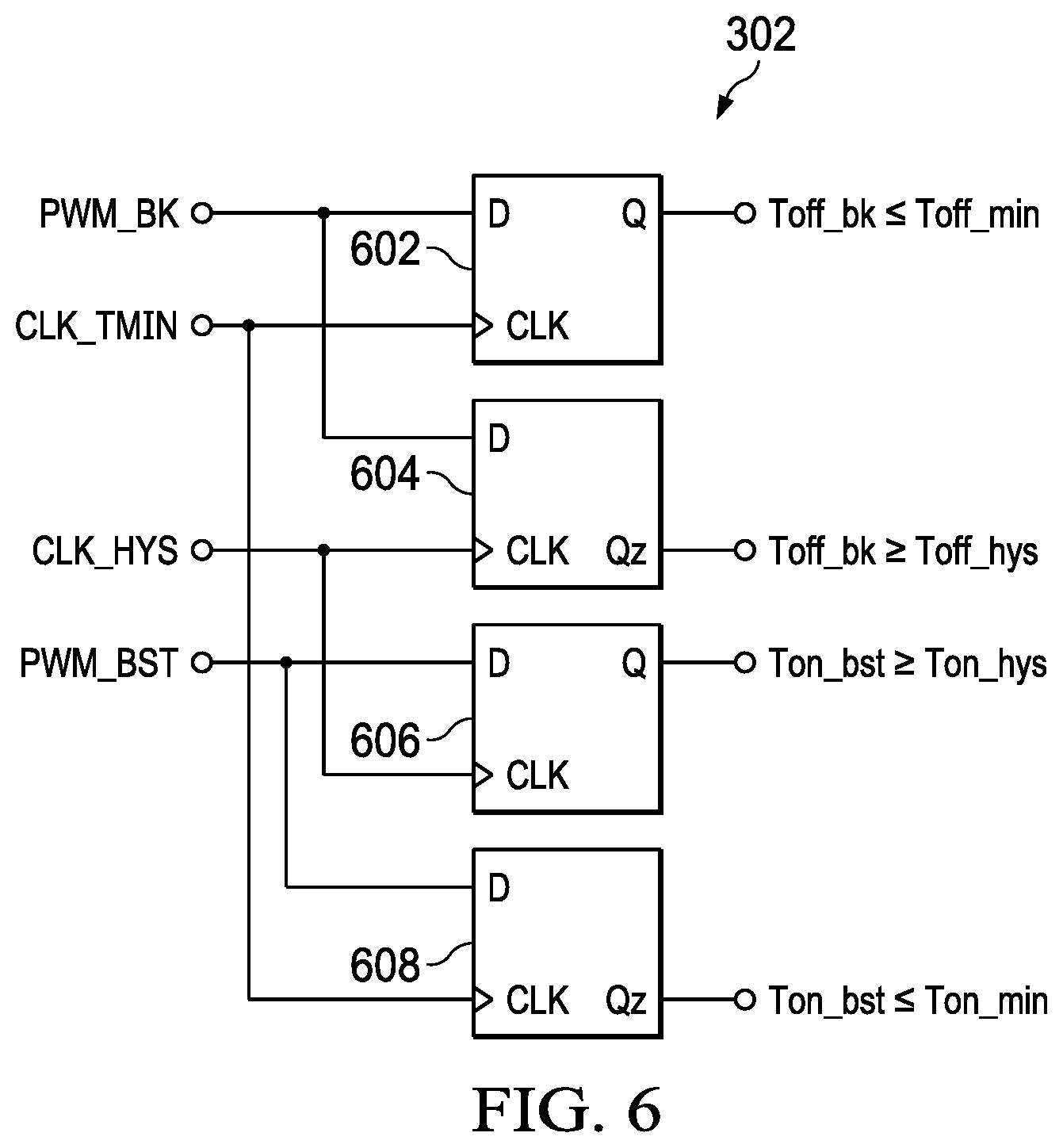
[0052] Returning now to FIG. 3, as discussed above, the timing detection circuit 302 makes a plurality of timing determinations and outputs a plurality of signals to the state machine circuit 308 indicating a result of a respective one of the timing determinations. Turning now to FIG. 6 a schematic diagram of an illustrative implementation of the timing detection circuit 302 is shown. Accordingly, the timing detection circuit 302 as shown in FIG. 3 is suitable for implementation in at least some examples of the mode transition control circuit 126 of FIG. 3. Therefore, reference may be made in describing FIG. 6 to at least some components and/or signals introduced and/or described above with respect to other figures of the present disclosure.
[0053] In at least one implementation, the timing detection circuit 302 includes a d flip-flop 602, a d flip-flop 604, a d flip-flop 606, and a d flip-flop 608. The d flip-flop 602, in at least some examples, is configured to receive PWM_BK at a data input terminal (indicated in FIG. 6 as D). The d flip-flop 602 is further configured to receive CLK_TMIN at a clock input terminal (indicated in FIG. 6 as CLK). The d flip-flop 602 outputs Toff_bk<=Toff_min at an output terminal (indicated in FIG. 6 as Q). In at least some examples, the data input terminal is coupled to the output terminal of the comparator 122 of FIG. 1, the clock input terminal is coupled to the timing generator 114, and the output terminal is coupled to the state machine circuit 308 of FIG. 3.
[0054] The d flip-flop 604, in at least some examples, is configured to receive PWM_BK at a data input terminal. The d flip-flop 604 is further configured to receive CLK_HYS at a clock input terminal. The d flip-flop 604 outputs Toff_bk>=Toff_hys at an inverse output terminal (indicated in FIG. 6 as Qz). In at least some examples, the data input terminal is coupled to the output terminal of the comparator 122 of FIG. 1, the clock input terminal is coupled to the oscillator 116, and the output terminal is coupled to the state machine circuit 308 of FIG. 3.
[0055] The d flip-flop 606, in at least some examples, is configured to receive PWM_BST at a data input terminal. The d flip-flop 606 is further configured to receive CLK_HYS at a clock input terminal. The d flip-flop 606 outputs Ton_bst>=Ton_hys at an output terminal. In at least some examples, the data input terminal is coupled to the output terminal of the comparator 124 of FIG. 1, the clock input terminal is coupled to the oscillator 116, and the output terminal is coupled to the state machine circuit 308 of FIG. 3.
[0056] The d flip-flop 608, in at least some examples, is configured to receive PWM_BST at a data input terminal. The d flip-flop 608 is further configured to receive CLK_TMIN at a clock input terminal. The d flip-flop 608 outputs Ton_bst<=Ton_min at an inverse output terminal. In at least some examples, the data input terminal is coupled to the output terminal of the comparator 124 of FIG. 1, the clock input terminal is coupled to the timing generator 114, and the output terminal is coupled to the state machine circuit 308 of FIG. 3.
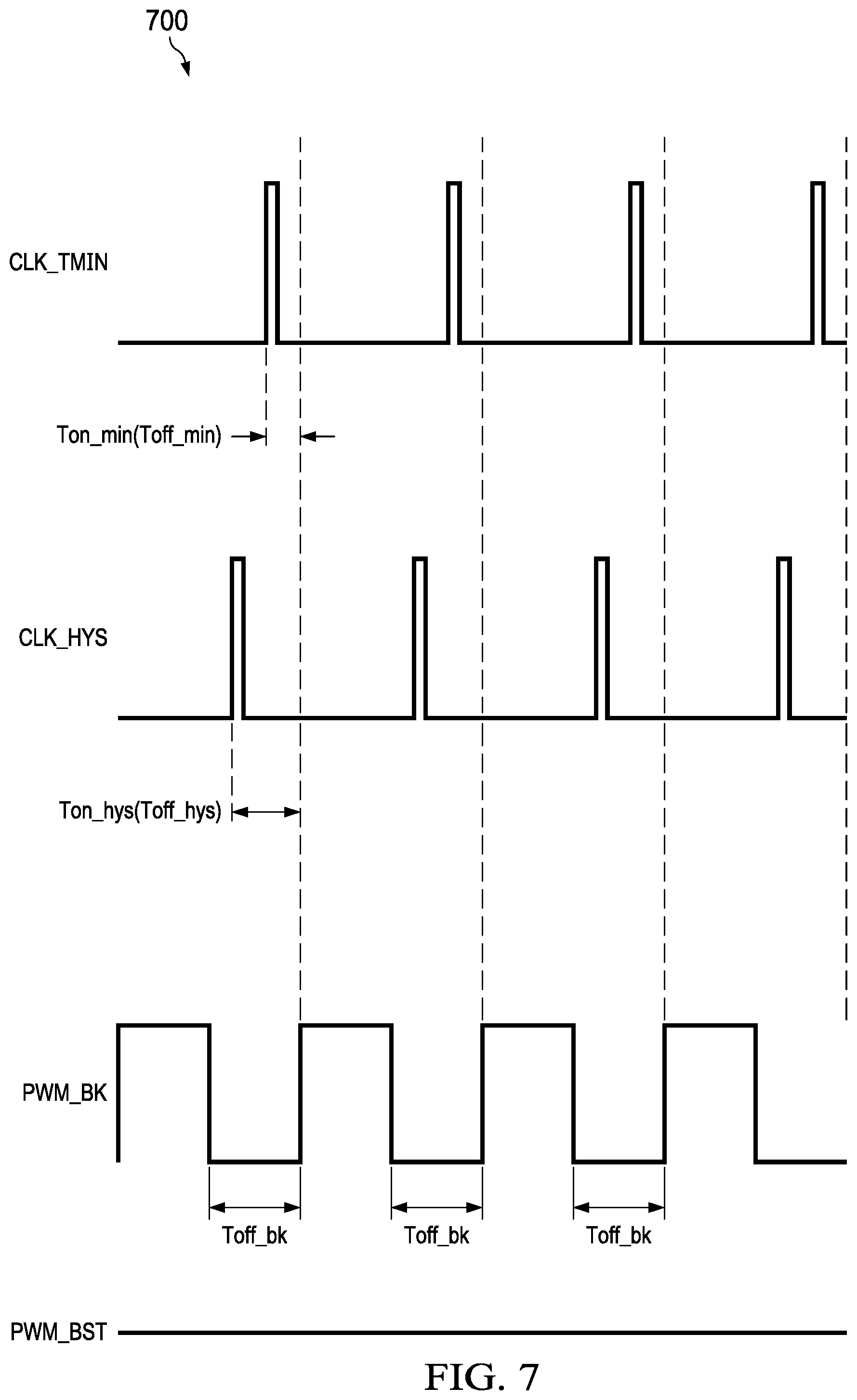
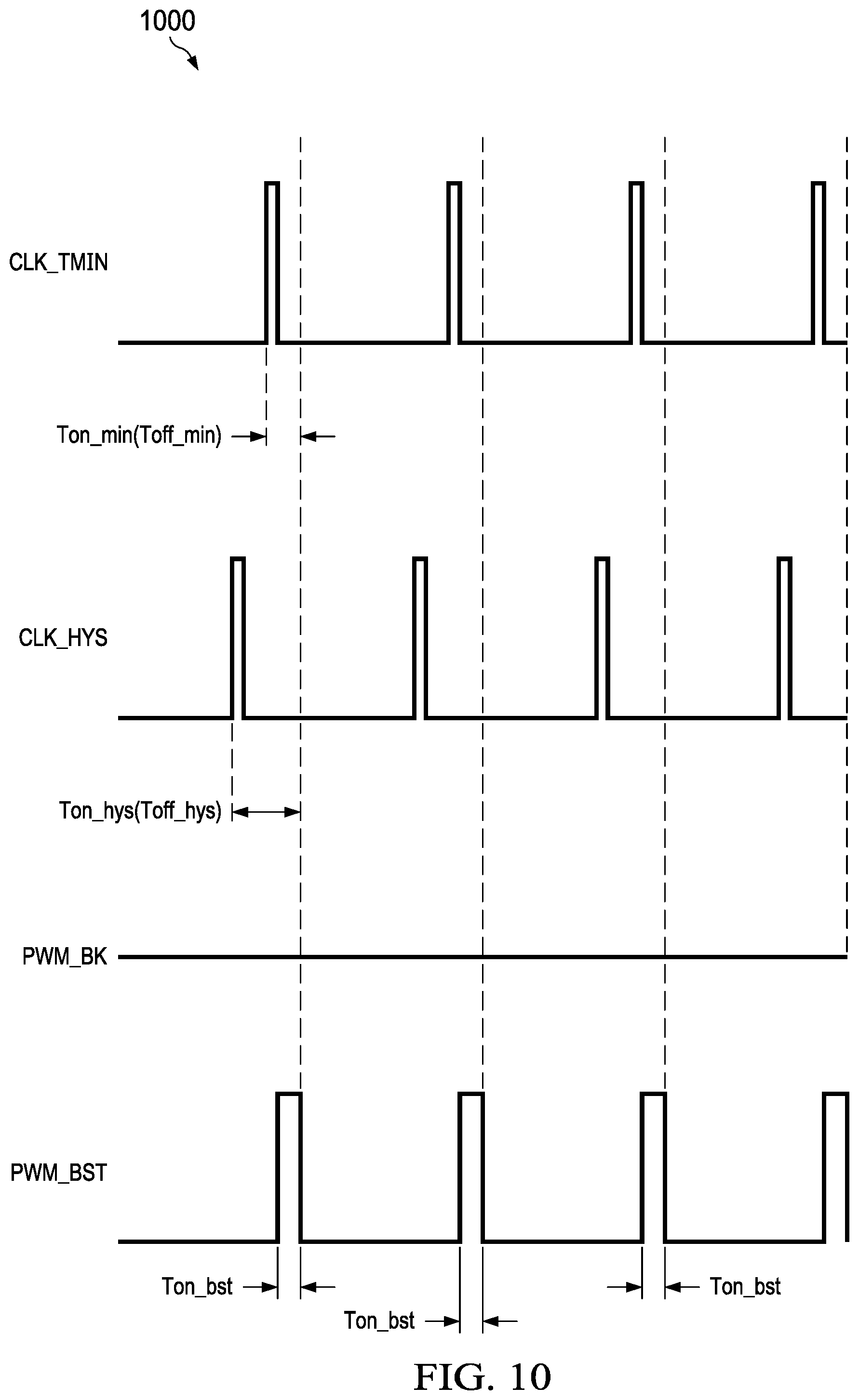
[0057] Based on values of PWM_BK, PWM_BST, CLK_TMIN, and CLK_HYS, the timing detection circuit 302 generates and outputs Toff bk<=Toff_min, Toff_bk>=Toff_hys, Ton_bst>=Ton_hys, and Ton_bst<=Ton_min. For example, turning now to FIGS. 7-10, various illustrative timing diagrams demonstrating operation of the timing detection circuit 302 are shown. As shown in FIGS. 7-10, a duration of time between a rising edge of CLK_TMIN and a rising edge of PWM_BK is Toff min. Similarly, a duration of time between a rising edge of CLK_TMIN and a falling edge of PWM_BST is Ton_min. A duration of time between a rising edge of CLK_HYS and a rising edge of PWM_BK is Toff_hys and a duration time between a rising edge of CLK_HYS and a falling edge of PWM_BST is Ton_hys.
[0058] For example, the timing diagram 700 of FIG. 7 illustrates generation of a control signal indicating that Toff bk is greater than Toff hys. As discussed above, the timing detection circuit 302 receives PWM_BK, PWM_BST, CLK_TMIN, and CLK_HYS. Based on a value of PWM_BK at a rising edge of CLK_HYS, the timing detection circuit 302 generates an output signal Toff_bk>Toff_hys. For example, when PWM_BK is de-asserted (e.g., in at least one example, has a logical low value) at a rising edge of CLK_HYS, the timing detection circuit 302 asserts Toff_bk>Toff_hys. In at least some examples, Toff_bk>=Toff_hys remains asserted until a next rising edge of PWM_BK.
[0059] The timing diagram 800 of FIG. 8 illustrates generation of a control signal indicating that Ton_bst is greater than Ton_hys. As discussed above, the timing detection circuit 302 receives PWM_BK, PWM_BST, CLK_TMIN, and CLK_HYS. Based on a value of PWM_BST at a rising edge of CLK_HYS, the timing detection circuit 302 generates an output signal Ton_bst>Ton_hys. For example, when PWM_BST is asserted (e.g., in at least one example, has a logical high value) at a rising edge of CLK_HYS, the timing detection circuit 302 asserts Ton_bst>Ton_hys. In at least some examples, Ton_bst>=Ton_hys remains asserted until a next rising edge of PWM_BST.
[0060] The timing diagram 900 of FIG. 9 illustrates generation of a control signal indicating that Toff_bk is less than or equal to Toff min. As discussed above, the timing detection circuit 302 receives PWM_BK, PWM_BST, CLK_TMIN, and CLK_HYS. Based on a value of PWM_BK at a rising edge of CLK_TMIN, the timing detection circuit 302 generates an output signal Toff_bk<=Toff_min. For example, when PWM_BK is asserted (e.g., in at least one example, has a logical high value) at a rising edge of CLK_TMIN, the timing detection circuit 302 asserts Toff_bk<=Toff_min. In at least some examples, Toff_bk<=Toff_min remains asserted until a next rising edge of PWM_BK.
[0061] The timing diagram 1000 of FIG. 10 illustrates generation of a control signal indicating that Ton_bst is less than or equal to Ton_min. As discussed above, the timing detection circuit 302 receives PWM_BK, PWM_BST, CLK_TMIN, and CLK_HYS. Based on a value of PWM_BST at a rising edge of CLK_TMIN, the timing detection circuit 302 generates an output signal Ton_bst<=Ton_min. For example, when PWM_BST is de-asserted (e.g., in at least one example, has a logical low value) at a rising edge of CLK_TMIN, the timing detection circuit 302 asserts Ton_bst<=Ton_min. In at least some examples, Ton_bst<=Ton_min remains asserted until a next rising edge of PWM_BST.
[0062] Turning now to FIG. 11, an illustrative timing diagram 1100 is shown. In at least some examples, the timing diagram 1100 illustrates at least some signals of the SMPS 100 of FIG. 1, discussed above. Therefore, reference may be made in describing FIG. 11 to at least some components and/or signals introduced and/or described above with respect to FIG. 1. The timing diagram 1100 illustrates CLK_HYS, as generated and output by the oscillator 116. As discussed above, the timing generator 114 generates CLK and CLK_TMIN by delaying or otherwise manipulating CLK_HYS. For example, as shown by the timing diagram 1100, the timing generator 114 manipulates CLK_HYS to generate CLK having a rising edge delayed by t.sub.hys from a rising edge of CLK_HYS. As further shown by the timing diagram 1100, the timing generator 114 manipulates CLK_HYS to generate CLK_TMIN having a rising edge delayed by t.sub.hys minus t.sub.min from a rising edge of CLK_HYS. In this way, the rising edge of CLK_TMIN precedes a rising edge of CLK by t.sub.min.
[0063] In the foregoing discussion, the terms "including" and "comprising" are used in an open-ended fashion, and thus should be interpreted to mean "including, but not limited to . . . ." The term "couple" is used throughout the specification. The term may cover connections, communications, or signal paths that enable a functional relationship consistent with the description of the present disclosure. For example, if device A generates a signal to control device B to perform an action, in a first example device A is coupled to device B, or in a second example device A is coupled to device B through intervening component C if intervening component C does not substantially alter the functional relationship between device A and device B such that device B is controlled by device A via the control signal generated by device A. A device that is "configured to" perform a task or function may be configured (e.g., programmed and/or hardwired) at a time of manufacturing by a manufacturer to perform the function and/or may be configurable (or re-configurable) by a user after manufacturing to perform the function and/or other additional or alternative functions. The configuring may be through firmware and/or software programming of the device, through a construction and/or layout of hardware components and interconnections of the device, or a combination thereof. Furthermore, a circuit or device that is said to include certain components may instead be configured to couple to those components to form the described circuitry or device. For example, a structure described as including one or more semiconductor elements (such as transistors), one or more passive elements (such as resistors, capacitors, and/or inductors), and/or one or more sources (such as voltage and/or current sources) may instead include only the semiconductor elements within a single physical device (e.g., a semiconductor die and/or integrated circuit (IC) package) and may be configured to couple to at least some of the passive elements and/or the sources to form the described structure either at a time of manufacture or after a time of manufacture, for example, by an end-user and/or a third-party.
[0064] While certain components are described herein as being of a particular process technology (e.g., FET, MOSFET, n-type, p-type, etc.), these components may be exchanged for components of other process technologies (e.g., replace FET and/or MOSFET with BJT, replace n-type with p-type or vice versa, etc.) and reconfiguring circuits including the replaced components to provide desired functionality at least partially similar to functionality available prior to the component replacement. Components illustrated as resistors, unless otherwise stated, are generally representative of any one or more elements coupled in series and/or parallel to provide an amount of impedance represented by the illustrated resistor. Additionally, uses of the phrase "ground voltage potential" in the foregoing discussion are intended to include a chassis ground, an Earth ground, a floating ground, a virtual ground, a digital ground, a common ground, and/or any other form of ground connection applicable to, or suitable for, the teachings of the present disclosure. Unless otherwise stated, "about", "approximately", or "substantially" preceding a value means +/-10 percent of the stated value.
[0065] The above discussion is meant to be illustrative of the principles and various examples of the present disclosure. Numerous variations and modifications will become apparent to those skilled in the art once the above disclosure is fully appreciated. It is intended that the present disclosure be interpreted to embrace all such variations and modifications.
* * * * *
D00000
D00001
D00002
D00003
D00004
D00005
D00006
D00007
D00008
D00009
D00010

XML
uspto.report is an independent third-party trademark research tool that is not affiliated, endorsed, or sponsored by the United States Patent and Trademark Office (USPTO) or any other governmental organization. The information provided by uspto.report is based on publicly available data at the time of writing and is intended for informational purposes only.
While we strive to provide accurate and up-to-date information, we do not guarantee the accuracy, completeness, reliability, or suitability of the information displayed on this site. The use of this site is at your own risk. Any reliance you place on such information is therefore strictly at your own risk.
All official trademark data, including owner information, should be verified by visiting the official USPTO website at www.uspto.gov. This site is not intended to replace professional legal advice and should not be used as a substitute for consulting with a legal professional who is knowledgeable about trademark law.