Method Of Depositing Material Onto A Surface And Structure Formed According To The Method
Ueda; Shinya
U.S. patent application number 16/867385 was filed with the patent office on 2020-11-12 for method of depositing material onto a surface and structure formed according to the method. The applicant listed for this patent is ASM IP Holding B.V.. Invention is credited to Shinya Ueda.
| Application Number | 20200357631 16/867385 |
| Document ID | / |
| Family ID | 1000004854450 |
| Filed Date | 2020-11-12 |


| United States Patent Application | 20200357631 |
| Kind Code | A1 |
| Ueda; Shinya | November 12, 2020 |
METHOD OF DEPOSITING MATERIAL ONTO A SURFACE AND STRUCTURE FORMED ACCORDING TO THE METHOD
Abstract
Methods of depositing material on a surface of a substrate are disclosed. The methods include exposing a surface of the substrate to a precursor within a reaction chamber to form adsorbed species on the surface and removing at least a portion of the adsorbed species prior to introducing a reactant to the reaction chamber.
| Inventors: | Ueda; Shinya; (Tokyo, JP) | ||||||||||
| Applicant: |
|
||||||||||
|---|---|---|---|---|---|---|---|---|---|---|---|
| Family ID: | 1000004854450 | ||||||||||
| Appl. No.: | 16/867385 | ||||||||||
| Filed: | May 5, 2020 |
Related U.S. Patent Documents
| Application Number | Filing Date | Patent Number | ||
|---|---|---|---|---|
| 62846424 | May 10, 2019 | |||
| Current U.S. Class: | 1/1 |
| Current CPC Class: | H01J 37/32834 20130101; H01L 21/0217 20130101; H01L 21/02167 20130101; H01L 21/02126 20130101; H01L 21/0214 20130101; H01J 37/32357 20130101; C23C 16/45536 20130101; H01J 2237/332 20130101; H01L 21/02189 20130101; H01L 21/02164 20130101; H01L 21/02186 20130101; H01L 21/0228 20130101; C23C 14/0036 20130101; H01L 21/02274 20130101 |
| International Class: | H01L 21/02 20060101 H01L021/02; H01J 37/32 20060101 H01J037/32; C23C 16/455 20060101 C23C016/455; C23C 14/00 20060101 C23C014/00 |
Claims
1. A method of depositing material onto a surface of a substrate, the method comprising the steps of: providing a substrate within a reaction chamber; exposing a surface of the substrate to a precursor, wherein the precursor reacts with species on the surface to form adsorbed species; removing a portion of the adsorbed species, leaving residual species on the surface; and providing a reactant to the reaction chamber, wherein the reactant reacts with the residual species to form the material.
2. The method of claim 1, wherein the step of removing comprises sputtering.
3. The method of claim 2, wherein the sputtering comprises using an activated species formed from an inert gas.
4. The method of claim 3, wherein the inert gas is selected from one or more gases of the group consisting of argon, helium, neon, krypton, and xenon.
5. The method of claim 1, wherein during the step of removing, a plasma is formed.
6. The method of claim 5, wherein the plasma is formed using a direct plasma system.
7. The method of claim 5, wherein the plasma is formed using a remote plasma system.
8. The method of claim 1, further comprising forming a plasma during at least a portion of the step of providing the reactant to the reaction chamber.
9. The method of claim 1, wherein the precursor and the reactant are provided to the reaction chamber during at least a portion of a precursor pulse interval.
10. The method of claim 1, wherein a purge gas is continuously provided to the reaction chamber during the steps of exposing the surface of the substrate to a precursor, removing a portion of the adsorbed species, and providing the reactant to the reaction chamber.
11. The method of claim 1, further comprising a step of purging the precursor from the reaction chamber, wherein the step of purging comprises providing an inert gas and the reactant to the reaction chamber.
12. The method of claim 1, wherein the precursor has a general formula of MpCqNrOsBtXuHv, wherein p, q, r, s, t, u, v are integers including zero, M comprises B, Si, Ti, or Zr, and X comprises F, Cl, Br, or I.
13. The method of claim 1, wherein the reactant is selected from one or more of the group consisting of O.sub.2, O.sub.3, CO.sub.2, N.sub.2O, N.sub.2, NH.sub.3, H.sub.2, CH.sub.4, and other hydrocarbons.
14. A method of depositing material onto a surface of a substrate, the method comprising the steps of: providing a substrate within a reaction chamber; providing a precursor to the reaction chamber for a precursor pulse interval to form adsorbed species on a surface of the substrate; purging the reaction chamber; removing a portion of the adsorbed species and leaving residual species on the surface; and providing a reactant for forming activated reactant species to the reaction chamber, wherein the activated reactant species react with the residual species to form the material.
15. The method of claim 14, wherein the step of removing a portion of the adsorbed species comprises sputtering.
16. The method of claim 15, wherein a power applied to generate a plasma during the step of sputtering is between about 50 W and about 2000 W.
17. The method of claim 15, wherein the sputtering comprises using an activated species formed from an inert gas.
18. The method of claim 17, wherein the inert gas is selected from one or more gases of the group consisting of argon, helium, neon, krypton, and xenon.
19. The method of claim 14, wherein a temperature within the reaction chamber during the step of removing a portion of the adsorbed species is between about -30.degree. C. and about 650.degree. C.
20. A deposition apparatus configured to perform the method of claim 1.
21. A device structure comprising a layer deposited according to the method of claim 1.
Description
CROSS-REFERENCE TO RELATED APPLICATIONS
[0001] This application claims the benefit of U.S. Provisional Patent Application No. 62/846,424 filed on May 10, 2019, the disclosure of which is incorporated herein in its entirety by reference.
FIELD OF INVENTION
[0002] The present disclosure generally relates to methods of depositing material onto a surface of a substrate, to structures formed using the method, and to systems for depositing the material.
BACKGROUND OF THE DISCLOSURE
[0003] Conformal film deposition may be desirable for a variety of reasons. For example, during the manufacture of devices, such as semiconductor devices, it is often desirable to conformally deposit material over features formed on the surface of a substrate. Such techniques can be used for shallow trench isolation, inter-metal dielectric layers, passivation layers, and the like. However, with miniaturization of devices, it becomes increasingly difficult to conformally deposit material, particularly over high aspect ratio features, such as features having an aspect ratio of three or more.
[0004] Atomic layer deposition (ALD) can be used to conformally deposit material onto a surface of a substrate. For some applications, such as when precursors and/or reactants otherwise require a relatively high temperature for ALD deposition and/or when it is desired to keep a processing temperature relatively low, it may be desirable to use plasma-enhanced ALD (PE-ALD).
[0005] Unfortunately, material deposited using PE-ALD on high aspect-ratio features tends to exhibit poor conformality/poor step coverage, because less material is deposited at the bottom of a feature (e.g., a trench or via), compared to at or near the top of the feature. The poor conformality of the deposited material can be attributed to a loss of activated species, such as radicals, that can occur by surface recombination of the radicals at, for example, the sidewalls of the features.
[0006] Efforts to improve low conformality of PE-ALD deposited material have focused on tuning process parameters, such as RF power, plasma exposure time, pressure, and the like, so as to provide adequate activated species, such as radicals, near the bottom of a feature, so as to increase an amount of material deposited at the bottom of the feature. However, because recombination of radicals is an intrinsic phenomenon, such efforts have been limited. And moreover, recent device manufacturing specifications often demand low plasma near the bottom of a feature. For such applications, conventional methods that include increasing activated species and/or activated species energy at the bottom of a feature cannot be used.
[0007] To overcome such problems, several techniques have been proposed. For example, U.S. Pat. No. 9,887,082 to Pore et al. discloses a method for filling a gap. The method includes providing a precursor into a reaction chamber to form adsorbed species on a surface of a substrate, exposing the adsorbed species to a nitrogen plasma to form species at the top of the feature that include nitrogen, and providing a reactant plasma to the reaction chamber, wherein nitrogen acts as an inhibitor to the reactant, resulting in less material being deposited at the top of the feature, compared to traditional PE-ALD techniques. However, it is often difficult to find suitable combinations of an inhibitor for desired reactant activated species.
[0008] U.S. Pat. No. 8,569,184, to Oka et al. discloses another PE-ALD processes. The method of Oka et al. includes a precursor feed step, wherein the precursor includes silicon and a non-metal element (such as N, C, B), which is adsorbed onto a substrate surface; an inert gas plasma exposure step, wherein the precursor is decomposed by inert gas plasma; and a reactant plasma exposure step. The decomposed precursor is oxidized to be complex anion compound of silicon. However, this process may not adequately address concerns of using conventional PE-ALD methods.
[0009] Accordingly, improved methods for conformally depositing material onto a substrate and structures formed using such methods are desired. Any discussion of problems and solutions involved in the related art has been included in this disclosure solely for the purposes of providing a context for the present invention and should not be taken as an admission that any or all of the discussion were known at the time the invention was made.
SUMMARY OF THE DISCLOSURE
[0010] Various embodiments of the present disclosure relate to methods of depositing material onto a surface of a substrate-e.g., conformally depositing material over features on the substrate surface. While the ways in which various embodiments of the present disclosure address drawbacks of prior methods and systems are discussed in more detail below, in general, various embodiments of the disclosure provide improved methods suitable for conformally depositing material over high aspect ratio features on a surface of a substrate, while mitigating any plasma-related damage at or near bottoms of the features.
[0011] Exemplary methods include adsorbing a precursor onto a surface of a substrate and removing a portion of the adsorbed precursor--e.g., by sputtering--prior to providing a reactant into the reaction chamber. Removing a portion of the adsorbed precursor slows the deposition rate and increases conformality of material deposited using PE-ALD, particularly in high-aspect ratio features.
[0012] In accordance with at least one embodiment of the disclosure, a method of depositing material onto a surface of a substrate includes providing a substrate within a reaction chamber; exposing a surface of the substrate to a precursor, such that the precursor reacts with species on the surface to form adsorbed species; removing a portion of the adsorbed species, leaving residual species on the surface; and providing a reactant to the reaction chamber, wherein the reactant reacts with the residual species to form the material. The step of removing can include, for example, sputtering. The sputtering can be performed using activated species of an inert gas, such as one or more of argon, helium, neon, krypton, and xenon. A direct or remote plasma system can be used during the step of removing. A direct or remote plasma system can also be used during a portion or all of the step of providing a reactant to the reaction chamber. In accordance with some aspects, the precursor and the reactant can be provided to the reaction chamber during at least a portion of a precursor pulse interval--i.e., a time interval in which the precursor is supplied to the reaction chamber. Exemplary methods can also include steps of purging the reaction chamber--e.g., after exposing a surface of the substrate to a precursor and/or after providing a reactant to the reaction chamber--using a vacuum source and/or a purge gas, such as argon, helium, neon, krypton, and/or xenon. Additionally, the reactant (e.g., without being exposed to a plasma) can be used to facilitate purging of the precursor. In accordance with some examples, a purge gas is continuously provided to the reaction chamber during the steps of exposing the surface of the substrate to a precursor, removing a portion of the adsorbed species, and providing the reactant to the reaction chamber.
[0013] In accordance with yet further exemplary embodiments of the disclosure, a deposition apparatus configured to perform a method as described herein is provided.
[0014] In accordance with yet further exemplary embodiments of the disclosure, a device structure comprises a layer deposited according to a method described herein.
[0015] These and other embodiments will become readily apparent to those skilled in the art from the following detailed description of certain embodiments having reference to the attached figures; the invention not being limited to any particular embodiment(s) disclosed.
BRIEF DESCRIPTION OF THE DRAWING FIGURES
[0016] A more complete understanding of exemplary embodiments of the present disclosure can be derived by referring to the detailed description and claims when considered in connection with the following illustrative figures.
[0017] FIG. 1 illustrates a method of depositing material in accordance with at least one embodiment of the disclosure.
[0018] FIGS. 2-4 illustrate structures formed in accordance with at least one embodiment of the disclosure.
[0019] FIG. 5 illustrates a method in accordance with at least one embodiment of the disclosure.
[0020] FIG. 6 illustrates adsorption states of a precursor in accordance with at least one embodiment of the disclosure.
[0021] FIG. 7 illustrates a timing sequence for deposition of material in accordance with exemplary embodiments of the disclosure.
[0022] FIG. 8 illustrates a schematic view of a PE-ALD apparatus in accordance with exemplary embodiments of the disclosure.
[0023] FIG. 9 illustrates a precursor supply system using a flow-pass system (FPS) according to an embodiment of the present disclosure.
[0024] It will be appreciated that elements in the figures are illustrated for simplicity and clarity and have not necessarily been drawn to scale. For example, the dimensions of some of the elements in the figures may be exaggerated relative to other elements to help improve understanding of illustrated embodiments of the present disclosure.
DETAILED DESCRIPTION OF EXEMPLARY EMBODIMENTS
[0025] Although certain embodiments and examples are disclosed below, it will be understood by those in the art that the invention extends beyond the specifically disclosed embodiments and/or uses of the invention and obvious modifications and equivalents thereof. Thus, it is intended that the scope of the invention disclosed should not be limited by the particular disclosed embodiments described below.
[0026] The present disclosure generally relates to methods of depositing material onto a surface of a substrate, to deposition apparatus for performing the methods, and to structures formed using the method. The methods as described herein can be used to process substrates, such as semiconductor wafers, to form, for example, electronic devices. By way of examples, the systems and methods described herein can be used to conformally deposit material onto a surface of a substrate, which can include high-aspect ratio features.
[0027] In this disclosure, "gas" may include material that is a gas at room temperature and pressure, a vaporized solid and/or a vaporized liquid, and may be constituted by a single gas or a mixture of gases, depending on the context. A gas other than the process gas, i.e., a gas introduced without passing through a gas distribution assembly, such as a showerhead, other gas distribution device, or the like, may be used for, e.g., sealing the reaction space, which includes a seal gas such as a rare gas. In some embodiments, the term "precursor" refers generally to a compound that participates in the chemical reaction that produces another compound, and particularly to a compound that constitutes a film matrix or a main skeleton of a film, whereas the term "reactant" refers to a compound, other than precursors, that activates a precursor, modifies a precursor, or catalyzes a reaction of a precursor, wherein the reactant may provide an element (such as O, N, C) to a film matrix and become a part of the film matrix, when RF power is applied. The term "inert gas" refers to a gas that does not take part in a chemical reaction and/or a gas that excites a precursor when RF power is applied, but unlike a reactant, it may not become a part of a film matrix to an appreciable extent.
[0028] As used herein, the term "substrate" may refer to any underlying material or materials that may be used to form, or upon which, a device, a circuit, or a film may be formed. A substrate can include a bulk material, such as silicon (e.g., single-crystal silicon), other Group IV materials, such as germanium, or compound semiconductor materials, such as GaAs, and can include one or more layers overlying or underlying the bulk material. Further, the substrate can include various topologies, such as recesses, lines, and the like formed within or on at least a portion of a layer of the substrate.
[0029] In some embodiments, "film" refers to a layer continuously extending in a direction perpendicular to a thickness direction substantially without pinholes to cover an entire target or concerned surface, or simply a layer covering a target or concerned surface. In some embodiments, "layer" refers to a structure having a certain thickness formed on a surface or a synonym of film or a non-film structure. A film or layer may be constituted by a discrete single film or layer having certain characteristics or multiple films or layers, and a boundary between adjacent films or layers may or may not be clear and may or may not be established based on physical, chemical, and/or any other characteristics, formation processes or sequence, and/or functions or purposes of the adjacent films or layers.
[0030] As used herein, the term "atomic layer deposition" (ALD) may refer to a vapor deposition process in which deposition cycles, preferably a plurality of consecutive deposition cycles, are conducted in a process chamber. Typically, during each cycle, the precursor is chemisorbed to a deposition surface (e.g., a substrate surface or a previously deposited underlying surface such as material from a previous ALD cycle), forming a monolayer or sub-monolayer that does not readily react with additional precursor (i.e., a self-limiting reaction). Thereafter, a reactant (e.g., another precursor or reaction gas) may subsequently be introduced into the process chamber for use in converting the chemisorbed precursor to the desired material on the deposition surface. Typically, this reactant is capable of further reaction with the precursor. Further, purging steps may also be utilized during each cycle to remove excess precursor from the process chamber and/or remove excess reactant and/or reaction byproducts from the process chamber after conversion of the chemisorbed precursor. Further, the term "atomic layer deposition," as used herein, is also meant to include processes designated by related terms, such as chemical vapor atomic layer deposition, atomic layer epitaxy (ALE), molecular beam epitaxy (MBE), gas source MBE, or organometallic MBE, and chemical beam epitaxy when performed with alternating pulses of precursor composition(s), reactive gas, and purge (e.g., inert carrier) gas. PE-ALD refers to an ALD process, in which a plasma is applied during one or more of the ALD steps.
[0031] Further, in this disclosure, any two numbers of a variable can constitute a workable range of the variable as the workable range can be determined based on routine work, and any ranges indicated may include or exclude the endpoints. Additionally, any values of variables indicated (regardless of whether they are indicated with "about" or not) may refer to precise values or approximate values and include equivalents, and may refer to average, median, representative, majority, etc. in some embodiments. Further, in this disclosure, the terms "constituted by" and "having" refer independently to "typically or broadly comprising," "comprising," "consisting essentially of," or "consisting of" in some embodiments. In this disclosure, any defined meanings do not necessarily exclude ordinary and customary meanings in some embodiments.
[0032] In this disclosure, "continuously" can refer to one or more of without breaking a vacuum, without interruption as a timeline, without any material intervening step, without changing treatment conditions, immediately thereafter, as a next step, or without an intervening discrete physical or chemical structure between two structures other than the two structures in some embodiments.
[0033] Turning now to the figures, FIG. 1 illustrates a method 100 in accordance with at least one embodiment of the disclosure. Method 100 includes the steps of providing a substrate within a reaction chamber (step 102), exposing a surface of the substrate to a precursor (step 104), removing a portion of the adsorbed species (step 108), and providing a reactant to the reaction chamber (step 110). As illustrated, method 100 can also include one or more purging steps (step 106 and/or step 112). Method 100 can include an ALD process, such as a PE-ALD process.
[0034] Step 102 includes providing at least one substrate into a reaction chamber and bringing the substrate to a desired deposition temperature. The reaction chamber may comprise PE-ALD reaction chamber, available from, for example, ASM International N.V. A temperature within the reaction chamber during step 102 can be brought to a temperature for subsequent processing--e.g., between about -30.degree. C. and about 650.degree. C. or about 50.degree. C. to about 500.degree. C. Similarly, a pressure within the reaction chamber may be controlled to provide a reduced atmosphere in the reaction chamber for subsequent processing. For example, the pressure within the reaction chamber can be brought to less than 5000 Pa, or less than 2000 Pa, or less than 1000 Pa, or be between about 100 and about 3000 Pa or about 200 and about 1000 Pa or about 300 and about 500 Pa.
[0035] During step 104, a surface of a substrate is exposed to a precursor. During this step, the temperature and/or pressure can be as set forth above in connection with step 102. The precursor can react with species on a surface of a substrate to form adsorbed species. Exemplary precursors suitable for use with step 104 include compounds having a general formula of MpCqNrOsBtXuHv, wherein p, q, r, s, t, u, v are integers including zero, wherein M is B, Si, Ti, or Zr; X is F, Cl, Br, or I; and C, H, N, O, B, represent their respective elements. By way of particular examples, one or more precursors can be selected to obtain a target compound, such as SiO, SiN, SiC, SiOC, SiON, TiO, TiN, ZrO, BN. Particular exemplary precursors include bis(dimethylamino) silane, bis(diethylamino) silane, tris(dimethylamino) cyclopentadienyl zirconium, Ti[N(CH.sub.3).sub.2].sub.4, Si(OC.sub.2H.sub.5).sub.4, P(CH.sub.3O).sub.3, B(CH.sub.3O).sub.3, PO(CH.sub.3O.sub.3), B(OC.sub.2H.sub.5).sub.3), Si(CH.sub.3).sub.2(OCH.sub.3).sub.2,
[0036] SiH(CH.sub.3).sub.3, Si(CH.sub.3).sub.4, and the like. Exemplary gas flow rates during step 104 can be about 500 sccm to about 20000 sccm or about 1000 sccm to about 4000 sccm. A pulse time for precursor flow during step 104 can be about 0.05 seconds to about 10 seconds or about 0.1 seconds to about 3 seconds.
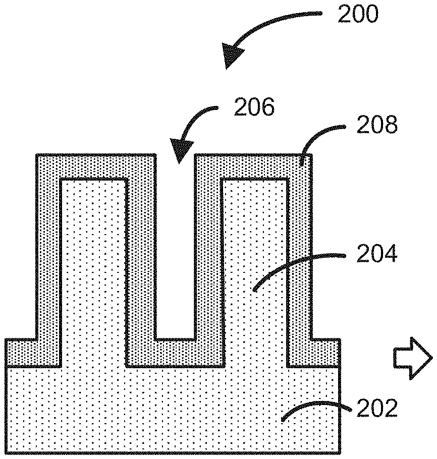
[0037] FIG. 2 illustrates a structure 200, which includes a substrate 202, including features 204 having a gap or recess 206 therebetween, and adsorbed species 208 on the surface of substrate 202, which can be formed according to step 104. As illustrated, adsorbed species 208 can be conformally adsorbed onto the surface of substrate 202 over features with relatively high aspect ratio of, for example, greater than 2, greater than 5, greater than 10, or between about 2 and about 30 or between about 5 and about 20. The adsorbed species can form, for example, about one monolayer of species on the surface of substrate 202.
[0038] Referring again to FIG. 1, step 108 includes removing a portion of the adsorbed species (e.g., adsorbed species 208), leaving residual species on the surface of the substrate. In accordance with various examples of the disclosure, the portion of the adsorbed species is removed using sputtering--e.g., using a plasma formed of an inert gas, such as one or more gases of the group consisting of argon, helium, neon, krypton, and xenon. The plasma can be formed as a direct plasma or by using a remote plasma system coupled to the reaction chamber. A power used to form the plasma can be between about 50 W and about 2000 W, or between about 300 W and about 1500 W. The temperature and pressure within the reaction chamber can be the same as set forth above in connection with step 102. Exemplary gas flow rates during step 108 can be about 500 sccm to about 20000 sccm or about 1000 sccm to about 8000 sccm. A pulse time for the plasma during step 108 can be about 0.05 seconds to about 15 seconds or about 0.2 seconds to about 5 seconds.
[0039] FIG. 3 illustrates a structure 300 after completion of step 108, where the dotted line represents a boundary of the adsorbed species before the removal of the portion of adsorbed species. Structure 300 includes substrate 202 and residual species 302 on the surface of substrate 202.
[0040] As illustrated in FIG. 3, a power, a reaction chamber pressure, or other parameter, can be selected, such that the portion of the adsorbed species removed near a top 304 of feature 204 is greater than the portion of the adsorbed species removed near a bottom 306 of feature 204, such that an opening 308 is wider near top 304, relative to bottom 306. Removing more adsorbed species near top 304 relative to bottom 306 can facilitate filling opening or recess 206 without a gap or a seam in the deposited material, which may be desirable for many applications. Furthermore, damage near a bottom 306 can be mitigated or eliminated, because the sputtering can be controlled to occur and desirably occurs mainly or exclusively near top 304, relative to bottom 306.
[0041] At step 110, a reactant is provided to the reaction chamber. The reactant can react with the residual species to form the material. A pressure and/or temperature in the reaction chamber during step 110 can be the same or similar to the pressure and/or temperature set forth above in connection with step 102.
[0042] Exemplary reactants suitable for step 110 include one or more elements that are incorporated into the material. By way of examples, the reactant can include one or more of O.sub.2, O.sub.3, CO.sub.2, N.sub.2O, N.sub.2, NH.sub.3, H.sub.2, CH.sub.4, and other hydrocarbons. By way of particular examples, the reactant can be selected from one or more of the group consisting of O.sub.2, N.sub.2, CO.sub.2, N.sub.2O, NH.sub.3. Exemplary gas flow rates during step 110 can be about 500 sccm to about 20000 sccm or about 1000 sccm to about 8000 sccm.
[0043] FIG. 4 illustrates a structure 400 after step 110. Structure 400 includes substrate 202 and material 402 deposited thereon. Each cycle (steps 104-110) can deposit, for example, about one monolayer of material.
[0044] As noted above, method 100 can additionally include one or more purge steps 106, 112. During purge steps 106, 112, any excess precursor, reactant, or byproducts thereof, can be removed from the reaction chamber using a purge gas and/or with the aid of a vacuum, generated by a pumping system, in fluid communication with the reaction chamber. Exemplary purge gases include argon, helium, neon, krypton, and/or xenon. A phase is generally considered to immediately follow another phase if a purge (i.e., purging gas pulse) or other reactant removal step intervenes. Exemplary gas flow rates during steps 106, 112 can be about 500 sccm to about 20000 sccm or about 1000 sccm to about 8000 sccm. A duration for purge steps 106, 112 can be about 0.1 seconds to about 10 seconds or about 0.2 seconds to about 5 seconds.
[0045] Method steps 102-112 of method 100 can be repeated a number of time. For example, steps 102-112 can be repeated until recess 206 is filled with material 402. In some embodiments, method 100 can include repeating step 104 one or more times prior to performing step 108 and similarly may additionally or alternatively include repeating step 110 one or more times prior to repeating method 100.
[0046] FIG. 5 illustrates deposition of a silicon oxide using method 100. In the illustrated example, during step (a), a silicon precursor 502 is provided within a reaction chamber that includes a surface of a substrate 504. Silicon precursor 502 can include silicon and one or more ligands 508. During step (b), silicon precursor 502 reacts with surface 504 to form adsorbed species 510, which can include a ligand 508, wherein another ligand 508 is liberated. During step (c), a portion of adsorbed species 510 is removed. Then, during step (d), a reactant reacts with the adsorbed species to form material 512. Steps (a) and (b) can correspond to step 104, step (c) can correspond to step 108, and step (d) can correspond to step 110 of method 100. Although described in connection with a silicon precursor, the method illustrated in FIG. 5 can be similarly practiced with other precursors, such as those noted herein.
[0047] Use of methods 100 and 500 has several advantages over conventional PE-ALD processing, including:
[0048] High conformality and high gap-fill properties: Because the precursor can be etched mainly at the top of the features/pattern by a plasma, a thickness of the material at the top is effectively reduced, which results in high conformality, which can be useful for gap-fill process in which void-free/seamless fill between features is desired.
[0049] No impurity element: Inert gas, such as argon, helium, neon, krypton, and xenon, can be used for the removal of adsorbed species step; therefore, resulting in no or substantially no chemical reaction between impurity elements (from the plasma) and deposited material.
[0050] Low plasma damage/low oxidation of under-layer: Deposition with high power plasma or high oxidation condition is not needed, which are conventionally used for improving conformality of PE-ALD films on high aspect ratio patterns. Rather, plasma conditions are set to preferentially remove material at the top of the features.
[0051] Fast run-rate: This process can use only one removal step in addition to the usual PE-ALD steps. The removal step can add only several seconds to the deposition method.
[0052] FIG. 6 illustrates adsorption states of a particular precursor, bis(dimethylamino) silane, as an example. The precursor can react with --OH ligands at the surface of a substrate 602: (a) is the initial stage of precursor adsorption, and (b) is the chemical adsorption state which is after several meta-stable states are undergone. The bonding energy of the chemical adsorption state, (b), is about 2 eV, which is higher than the mean kinetic energy of Ar ion, .sup..about.1 eV, of Ar plasma etching. Therefore, dissociation of the precursor from (b) is not likely to occur. On the other hand, bonding energy of (a) and also of meta-stable states is less than 1 eV, therefore, dissociation of the precursor can occur by plasma sputtering (e.g., argon). Removal, such as by sputtering, as described herein can remove weakly adsorbed precursor from a substrate, and may not remove strongly bonded chemically adsorbed precursor. Therefore, it may be desirable to remove a portion of the adsorbed species that are in the state illustrated in (a).
[0053] FIG. 7 illustrates a timing sequence 700 for deposition of material in accordance with exemplary embodiments of the disclosure. The illustrated timing sequence 700 includes a precursor pulse step 702, a precursor purge step 704, an RF on (without a reactant flowing) step 706, an RF on (with reactant flowing) step 708, and a purge step 710.
[0054] Step 702 can be the same or similar to step 104. During step 702, an inert gas and optionally a reactant gas can flow. The precursor can be pulsed after the inert gas and/or reactant flow has started. At step 704, the precursor flow has ceased, and the reactant and/or inert gas continues to flow to facilitate purging of the reaction chamber. At step 706, a plasma is initiated, and the reactant gas does not flow. This allows removal of a portion of adsorbed species that form during step 702. Then, during step 708, the reactant flow is on, and activated reactant species are formed to react with residual species that remain after step 706 to form the material. Another purge step 710 with inert and/or reactant gas can be performed after step 708. Steps 702, 704, 706, 708, and 710 can be the same as steps 104, 106, 108, 110, and 112 described above. Further, steps 702-710 can be repeated as desired.
[0055] The methods described herein can be performed using any suitable apparatus including an apparatus illustrated in FIG. 8, for example. FIG. 8 is a schematic view of a PE-ALD apparatus, desirably in conjunction with controls programmed to conduct the sequences described herein, usable in at least some embodiments of the present invention. In the example illustrated in FIG. 8, by providing a pair of electrically conductive flat-plate electrodes 4, 2 in parallel and facing each other in the interior 11 (reaction zone) of a reaction chamber 3, applying RF power (e.g., 13.56 MHz or 27 MHz) from a power source 25 to one side, and electrically grounding the other side 12, a plasma is excited between the electrodes. A temperature regulator is provided in a lower stage 2 (the lower electrode), and a temperature of a substrate 1 placed thereon is kept constant at a given temperature. The upper electrode 4 can serve as a shower plate as well, and reactant gas and/or dilution gas, if any, and precursor gas can be introduced into the reaction chamber 3 through a gas line 21 and a gas line 22, respectively, and through the shower plate 4. Additionally, in the reaction chamber 3, a circular duct 13 with an exhaust line 7 is provided, through which gas in the interior 11 of the reaction chamber 3 is exhausted. Additionally, a transfer chamber 5 disposed below the reaction chamber 3 is provided with a seal gas line 24 to introduce seal gas into the interior 11 of the reaction chamber 3 via the interior 16 (transfer zone) of the transfer chamber 5 wherein a separation plate 14 for separating the reaction zone and the transfer zone is provided (a gate valve through which a wafer is transferred into or from the transfer chamber 5 is omitted from this figure). The transfer chamber is also provided with an exhaust line 6.
[0056] In some embodiments, in the apparatus depicted in FIG. 8, the system of switching flow of an inactive gas and flow of a precursor gas illustrated in FIG. 9 can be used to introduce the precursor gas in pulses without substantially fluctuating pressure of the reaction chamber. The continuous flow of the carrier gas can be accomplished using a flow-pass system (FPS) wherein a carrier gas line is provided with a detour line having a precursor reservoir (bottle), and the main line and the detour line are switched, wherein when only a carrier gas is intended to be fed to a reaction chamber, the detour line is closed, whereas when both the carrier gas and a precursor gas are intended to be fed to the reaction chamber, the main line is closed and the carrier gas flows through the detour line and flows out from the bottle together with the precursor gas. In this way, the carrier gas can continuously flow into the reaction chamber and can carry the precursor gas in pulses by switching the main line and the detour line. FIG. 9 illustrates a precursor supply system using a flow-pass system (FPS) according to an embodiment of the present disclosure (black valves indicate that the valves are closed). As shown in (a) in FIG. 9, when feeding a precursor to a reaction chamber (not shown), first, a carrier gas such as Ar (or He or the like) flows through a gas line with valves b and c, and then enters a bottle (reservoir) 20. The carrier gas flows out from the bottle 20 while carrying a precursor gas in an amount corresponding to a vapor pressure inside the bottle 20 and flows through a gas line with valves f and e and is then fed to the reaction chamber together with the precursor. In the above, valves a and d are closed. When feeding only the carrier gas (noble gas) to the reaction chamber, as shown in (b) in FIG. 9, the carrier gas flows through the gas line with the valve a while bypassing the bottle 20.
[0057] The example embodiments of the disclosure described above do not limit the scope of the invention, since these embodiments are merely examples of the embodiments of the invention. For example, although illustrated using sputtering, other techniques can be used to remove adsorbed species. Any equivalent embodiments are intended to be within the scope of this invention. Indeed, various modifications of the disclosure, in addition to those shown and described herein, such as alternative useful combinations of the elements described, may become apparent to those skilled in the art from the description. Such modifications and embodiments are also intended to fall within the scope of the appended claims.
[0058] What is claimed is:
* * * * *
D00000
D00001
D00002
D00003
D00004
D00005
D00006
XML
uspto.report is an independent third-party trademark research tool that is not affiliated, endorsed, or sponsored by the United States Patent and Trademark Office (USPTO) or any other governmental organization. The information provided by uspto.report is based on publicly available data at the time of writing and is intended for informational purposes only.
While we strive to provide accurate and up-to-date information, we do not guarantee the accuracy, completeness, reliability, or suitability of the information displayed on this site. The use of this site is at your own risk. Any reliance you place on such information is therefore strictly at your own risk.
All official trademark data, including owner information, should be verified by visiting the official USPTO website at www.uspto.gov. This site is not intended to replace professional legal advice and should not be used as a substitute for consulting with a legal professional who is knowledgeable about trademark law.