Magnetic Material and Magnetic Element
Wakabayashi; Yuki ; et al.
U.S. patent application number 16/963562 was filed with the patent office on 2020-11-12 for magnetic material and magnetic element. The applicant listed for this patent is Nippon Telegraph and Telephone Corporation. Invention is credited to Yoshiharu Krockenberger, Yoshitaka Taniyasu, Yuki Wakabayashi, Hideki Yamamoto.
| Application Number | 20200357555 16/963562 |
| Document ID | / |
| Family ID | 1000005032784 |
| Filed Date | 2020-11-12 |


| United States Patent Application | 20200357555 |
| Kind Code | A1 |
| Wakabayashi; Yuki ; et al. | November 12, 2020 |
Magnetic Material and Magnetic Element
Abstract
A magnetic material is constituted of a ferromagnetic or ferrimagnetic insulator in a double perovskite structure of Sr.sub.3-xA.sub.xOs.sub.1-yB.sub.yO.sub.6 (0.5.ltoreq.x.ltoreq.0.5, -0.5.ltoreq.y.ltoreq.0.5). A is an alkali metal or alkaline earth metal atom, and B is a transition metal atom, alkali metal atom, or alkaline earth metal atom). The insulator may be Sr.sub.3OsO.sub.6, where x=y=0 in the above formula. Sr.sub.3OsO.sub.6 is formed to have a cubic crystal structure where strontium atoms, osmium atoms, and oxygen atoms are arranged at lattice points.
| Inventors: | Wakabayashi; Yuki; (Tokyo, JP) ; Krockenberger; Yoshiharu; (Tokyo, JP) ; Yamamoto; Hideki; (Tokyo, JP) ; Taniyasu; Yoshitaka; (Tokyo, JP) | ||||||||||
| Applicant: |
|
||||||||||
|---|---|---|---|---|---|---|---|---|---|---|---|
| Family ID: | 1000005032784 | ||||||||||
| Appl. No.: | 16/963562 | ||||||||||
| Filed: | February 15, 2019 | ||||||||||
| PCT Filed: | February 15, 2019 | ||||||||||
| PCT NO: | PCT/JP2019/005561 | ||||||||||
| 371 Date: | July 21, 2020 |
| Current U.S. Class: | 1/1 |
| Current CPC Class: | C23C 14/28 20130101; H01F 10/18 20130101; H01F 41/205 20130101; C23C 14/08 20130101; C01P 2002/30 20130101; B82Y 25/00 20130101 |
| International Class: | H01F 10/18 20060101 H01F010/18 |
Foreign Application Data
| Date | Code | Application Number |
|---|---|---|
| Feb 16, 2018 | JP | 2018-025897 |
Claims
1.-4. (canceled)
5. A magnetic material which is constituted of: a ferromagnetic or ferrimagnetic insulator in a double perovskite structure of Sr.sub.3-xA.sub.xOs.sub.1-yB.sub.yO.sub.6; wherein -0.5.ltoreq.x.ltoreq.0.5; wherein -0.5.ltoreq.y.ltoreq.0.5; wherein A is an alkali metal or alkaline earth metal; wherein B is a transition metal, an alkali metal atom, or analkaline earth metal atom; and wherein an atomic percentage of Sr is in a range of 25 at % to 35 at %.
6. The magnetic material according to claim 5, wherein the ferromagnetic or ferrimagnetic insulator is constituted of Sr.sub.3OsO.sub.6.
7. The magnetic material according to claim 5, wherein: the ferromagnetic or ferrimagnetic insulator has a cubic crystal structure.
8. The magnetic material of claim 7, wherein a strontium atom is a lattice point of the cubic crystal structure.
9. The magnetic material of claim 7, wherein an osmium atom is a lattice point of the cubic crystal structure.
10. The magnetic material of claim 7, wherein an oxygen atom is a lattice point of the cubic crystal structure.
11. A magnetic device comprising: a magnetic layer made from a ferromagnetic insulator in a double perovskite structure of Sr.sub.3-xA.sub.xOs.sub.1-yB.sub.yO.sub.6, wherein -0.5.ltoreq.x.ltoreq.0.5, wherein -0.5.ltoreq.y.ltoreq.0.5, wherein A is an alkali metal or alkaline earth metal, wherein B is a transition metal, an alkali metal atom, or analkaline earth metal atom, and wherein an atomic percentage of Sr is in a range of 25 at % to 35 at %; a first electrode; and a second electrode, the magnetic layer is between the first electrode and the second electrode.
12. The magnetic device according to claim ii, wherein the ferromagnetic insulator is constituted of Sr.sub.3OsO.sub.6.
13. The magnetic device according to claim ii, wherein: the ferromagnetic insulator has a cubic crystal structure.
14. The magnetic device according to claim 13, wherein a strontium atom is a lattice point of the cubic crystal structure.
15. The magnetic device according to claim 13, wherein an osmium atom is a lattice point of the cubic crystal structure.
16. The magnetic device according to claim 13, wherein an oxygen atom is a lattice point of the cubic crystal structure.
Description
CROSS-REFERENCE TO RELATED APPLICATIONS
[0001] This application claims priority to National phase entry PCT/JP2019/005561, filed on Feb. 15, 2019, which claims priority to Japanese Patent Application No. 2018-025897, filed on Feb. 16, 2018, which applications are hereby incorporated herein by reference.
TECHNICAL FIELD
[0002] The present invention relates to a ferromagnetic or ferrimagnetic material, and a magnetic device using the same.
BACKGROUND
[0003] Ferromagnetic or ferrimagnetic materials that are insulators (which will be hereinafter referred to as ferromagnetic insulators) have the characteristic of a large specific electrical resistance compared with ferromagnetic metals, and are widely applied to permanent magnets, core materials, isolators and circulators, and so on. Typical properties (material properties) of the foregoing ferromagnetic insulators include Curie temperature (T.sub.C), initial permeability, relative loss factors, saturation magnetic flux density, and coercivity. Particularly, T.sub.C is a temperature above which ferromagnetism (or ferrimagnetism) is lost to lead to paramagnetism. As T.sub.C is higher, thermal stability is higher, which brings stable operation characteristics even at high temperatures.
[0004] Ferromagnetic insulators having a perovskite or double perovskite structure have the consistency with SrTiO.sub.3 (perovskite structure), which is a typical oxide electronics material, and thus are promising for the application to spin electronics using oxides [such as a magnetoresistive random access memory (MRAM) and spin MOSFET] (NPL 1).
[0005] Table 1 shows T.sub.C, saturation magnetization, and crystal forms of typical exiting ferromagnetic insulators (NPL 2). The highest T.sub.C is conventionally 943 K of LiFe.sub.5O.sub.8 having a spinel structure. As a ferromagnetic insulator having a double perovskite structure, Sr.sub.2CrOsO.sub.6 takes the maximum value of T.sub.C equal to 725 K.
TABLE-US-00001 TABLE 1 saturation material T.sub.c (K) magnetization (emu/cc) crystal form MuFe.sub.2O.sub.4 573 520 spinel NiFe.sub.2O.sub.4 863 340 spinel CoFe.sub.2O.sub.4 500 793 spinel CuFe.sub.2O.sub.4 728 170 spinel MgFe.sub.2O.sub.4 713 140 spinel LiFe.sub.5O.sub.8 943 390 spinel .gamma.-Fe.sub.2O.sub.3 848 520 spinel BaFe.sub.12O.sub.19 723 480 magnetoplumbite SrFe.sub.12O.sub.19 726 480 magnetoplumbite Y.sub.3Fe.sub.5O.sub.12 560 170 garnet Ca.sub.2FeReO.sub.6 520 double perovskite Sr.sub.2CrOsO.sub.6 725 double perovskite
CITATION LIST
Non Patent Literature
[0006] [NPL 1] S. Sugahara, and M. Tanaka, "A spin metal-oxide-semiconductor field-effect transistor using half-metallic-ferromagnet contacts for the source and drain", Applied Physics Letters, vol. 84, no. 13, pp. 2307-2309, 2004.
[0007] [NPL 2] P. D. BABA, et al., "Fabrication and Properties of Microwave Lithium Ferrites", IEEE Transactions on Magnetics, vol. MAG-8, no. 1, pp. 83-94, 1972.
SUMMARY
Technical Problem
[0008] The Curie temperatures of the foregoing conventional ferromagnetic insulators are however lower than a value required in order for spintronics devices to have high thermal stability, which is problematic.
[0009] Embodiments of the present invention was made to solve the foregoing problem, and an object thereof is to make it possible to realize a magnetic material having a higher Curie temperature.
Means for Solving the Problem
[0010] A magnetic material according to embodiments of the present invention is constituted of a ferromagnetic or ferrimagnetic insulator in a double perovskite structure of Sr.sub.3-xA.sub.xOs.sub.1-yB.sub.yO.sub.6 (-0.5.ltoreq.x.ltoreq.0.5, -0.5.ltoreq.y.ltoreq.0.5, A: an alkali metal or alkaline earth metal atom, B: a transition metal atom, alkali metal atom, or alkaline earth metal atom), wherein an atomic percentage of Sr is 25 to 35 at %.
[0011] In the magnetic material, the insulator is constituted of Sr.sub.3OsO.sub.6.
[0012] In the magnetic material, the insulator has a cubic crystal structure.
[0013] A magnetic device according to the present invention includes: a magnetic layer made from the foregoing ferromagnetic material; a first electrode; and a second electrode, the first and second electrodes being formed across the magnetic layer.
Effects of embodiments of the Invention
[0014] As described above, according to embodiments of the present invention, an insulator made from Sr.sub.3-xA.sub.xOs.sub.1-yB.sub.yO.sub.6 is used, which brings a fine effect, that is, a magnetic material having a higher Curie temperature can be realized.
BRIEF DESCRIPTION OF THE DRAWINGS
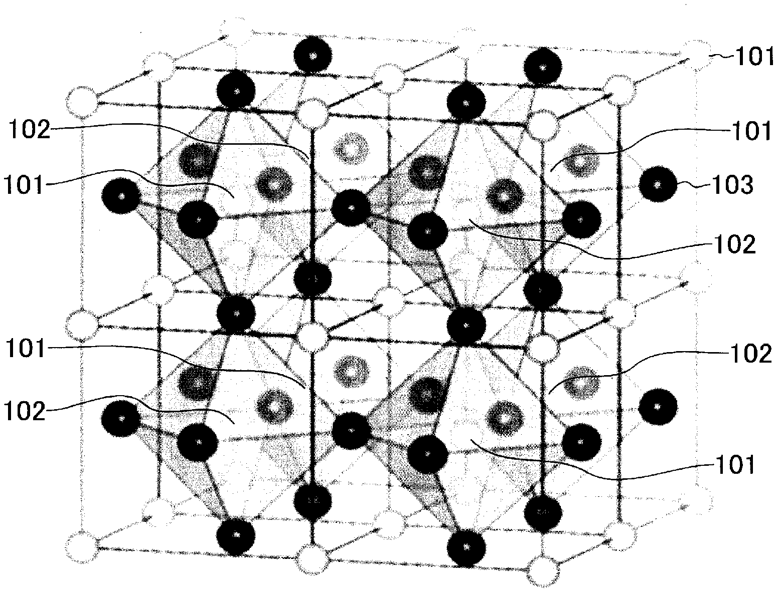
[0015] FIG. 1 is a perspective view of a crystal structure of Sr.sub.3OsO.sub.6 used as a magnetic material in the embodiments of the present invention.
[0016] FIG. 2 is a cross-sectional view showing a situation where a magnetic material layer 202 that is made from Sr.sub.3OsO.sub.6 is made on a growth substrate 201 that is made from SrTiO.sub.3(001).
[0017] FIG. 3 shows micrographs of high-angle annular dark-field scanning transmission electron microscope images of the magnetic material layer 202.
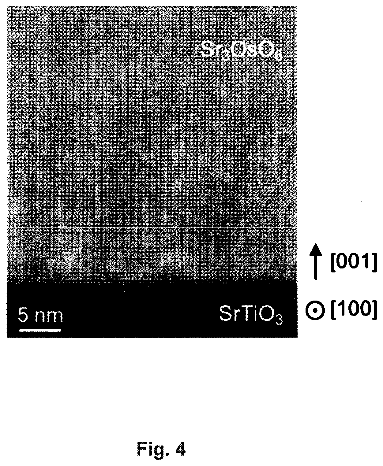
[0018] FIG. 4 shows a micrograph of a transmission electron microscopy image at the interface between the growth substrate 201 and the magnetic material layer 202.
[0019] FIG. 5 is a characteristic diagram showing temperature dependence of magnetization of the magnetic material layer 202 in a magnetic field at 2000 Oe.
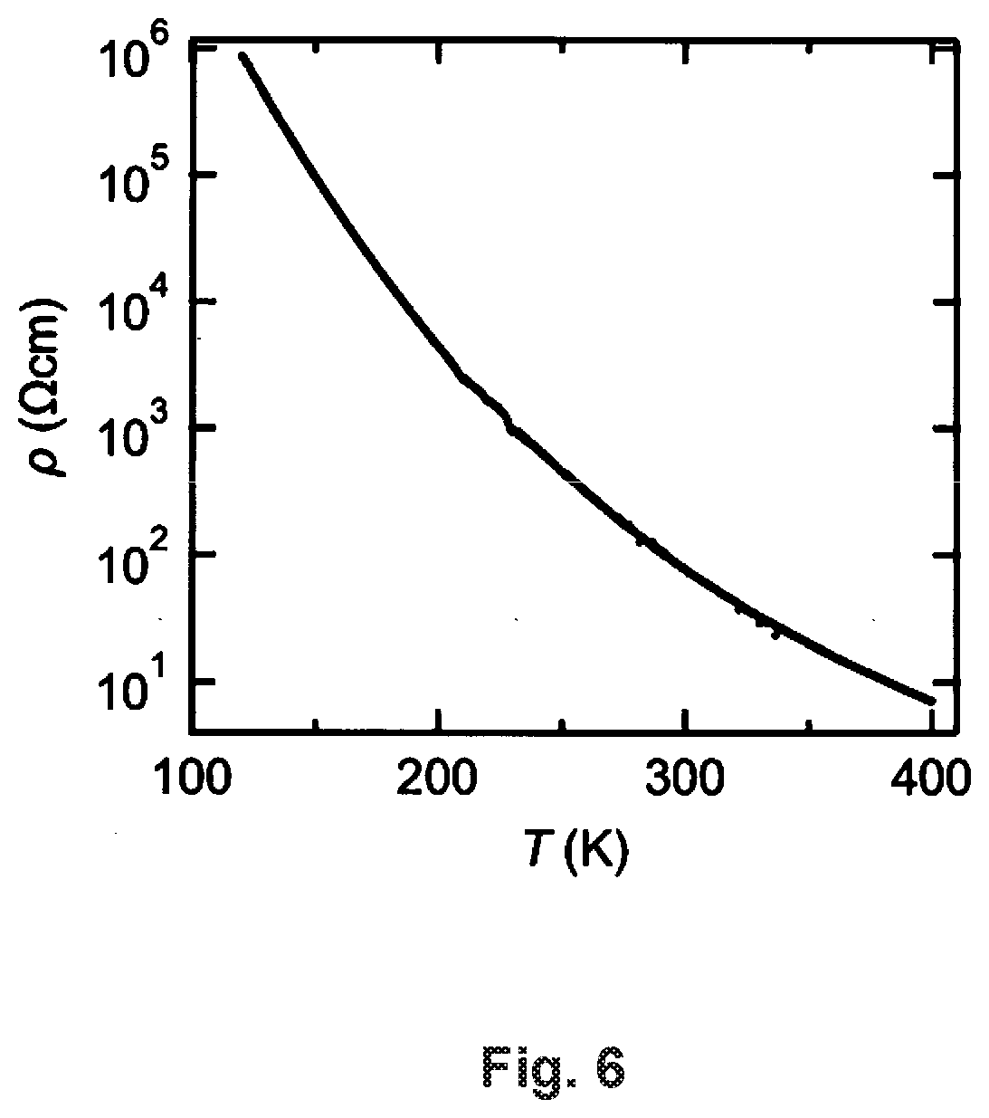
[0020] FIG. 6 is a characteristic diagram showing temperature dependence of specific electrical resistance (.rho.) of the magnetic material layer 202.
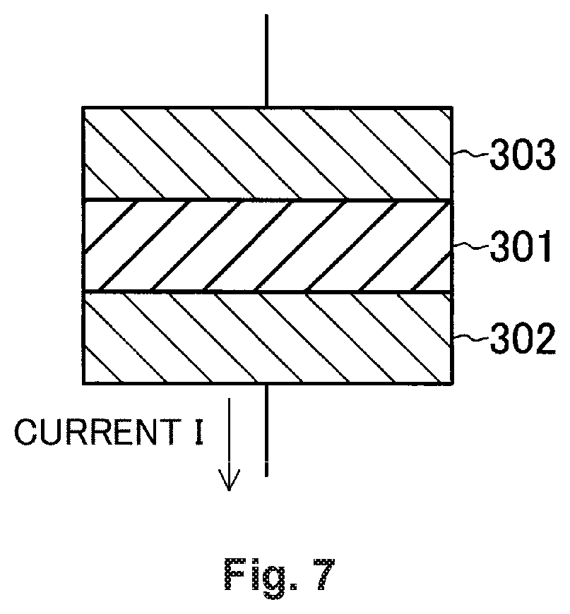
[0021] FIG. 7 is a cross-sectional view showing structure of a magnetic device in the embodiments of the present invention.
DETAILED DESCRIPTION OF ILLUSTRATIVE EMBODIMENTS
[0022] Hereinafter a magnetic material in the embodiments of the present invention will be described. This magnetic material is m is constituted of a ferromagnetic or ferrimagnetic insulator in a double perovskite structure of Sr.sub.3-xA.sub.xOs.sub.1-yB.sub.yO.sub.6 (-0.5.ltoreq.x.ltoreq.0.5, -0.5.ltoreq.y.ltoreq.0.5, A: an alkali metal or alkaline earth metal atom, B: a transition metal atom, alkali metal atom, or alkaline earth metal atom). In this magnetic material, the atomic percentage of Sr is 25 to 35 at %. Here, the foregoing insulator may be Sr.sub.3OsO.sub.6, which is Sr.sub.3-xA.sub.xOs.sub.1-yB.sub.yO.sub.6 where x=y=0.
[0023] In Sr.sub.3OsO.sub.6 constituting the magnetic material in the embodiments, strontium atoms 101, osmium atoms 102 and oxygen atoms 103 form a cubic crystal structure where lattice points are arranged as shown in FIG. 1. A magnetic material constituted of Sr.sub.3OsO.sub.6, which has the simplest composition, can be made only from three constituent elements (Sr, Os and O), and thus has the advantage of easy control of the composition thereof compared with the conventional ferromagnetic insulators having a double perovskite structure, each of which is constituted of four elements, shown in Table 1. The Curie temperature T.sub.C of the magnetic material in the embodiments which is constituted of Sr.sub.3OsO.sub.6 equals 1060 K. The foregoing crystal structure is not limited to the cubic crystal system, but may have a rhombic crystalline shape (the orthorhombic crystal system) or the tetragonal crystal system.
[0024] Hereinafter more detailed description will be made using the result of an experiment.
[0025] First, in the experiment, a magnetic material by Sr.sub.3OsO.sub.6 was made. As shown in FIG. 2, Sr.sub.3OsO.sub.6 was grown by well-known molecular beam epitaxy on a growth substrate 201 for growth which was made from SrTiO.sub.3(001), to form a magnetic material layer 202. A material such as MgO(001) and (La.sub.0.3Sr.sub.0.7)(Al.sub.0.65Ta.sub.0.35)O.sub.3(001) may be used for the growth substrate.
[0026] When the magnetic material layer 202 was formed by molecular beam epitaxy, the atomic beams of alkaline earth metal Sr and 5d transition metal Os were supplied in an ultra-high vacuum processing tank in the atmosphere of reactive oxygen species of approximately 10.sup.-6 Torr on the condition that the substrate temperature was 650.degree. C. so that a predetermined composition ratio is obtained, to grow Sr.sub.3OsO.sub.6. The magnetic material layer 202 was formed to have a layer thickness of 300 nm.
[0027] The result (microscopy image) of observation of the made magnetic material layer 202 by means of a high-angle annular dark-field scanning transmission electron microscope (HAADF-STEM) will be described using FIG. 3. FIG. 3(a) is an image obtained by means of an incident electron beam in the [100] direction to the magnetic material layer 202. FIG. 3(b) is an image obtained by means of an incident electron beam in the [110] direction to the magnetic material layer 202.
[0028] It is found that as shown in FIG. 3, Sr and Os atoms are arranged in a highly ordered manner in the magnetic material layer 202, to form a single crystal having a cubic double perovskite structure. The arrangement of oxygen atoms was confirmed by an annular bright-field scanning transmission electron microscopy (ABF-STEM) image. The fact that the made magnetic material layer 202 had a cubic double perovskite structure was also confirmed by reflection high energy electron diffraction (RHEED) measurement in vacuum molecular beam epitaxy equipment, and .theta.-2.theta. measurement of X-ray diffraction (XRD) in the air outside molecular beam epitaxy equipment.
[0029] FIG. 4 shows a transmission electron microscopy image at the interface between the growth substrate 201 and the magnetic material layer 202. It is found that single crystal growth of the magnetic material layer 202 from the growth substrate 201 epitaxially progresses. The relationships of the crystal orientation between the magnetic material layer 202 and the growth substrate 201 were such as Sr.sub.3OsO.sub.6[001]//SrTiO.sub.3[001] and Sr.sub.3OsO.sub.6[100]//SrTiO.sub.3[100].
[0030] FIG. 5 shows temperature dependence of magnetization of the magnetic material layer 202 in a magnetic field at 2000 Oe. There still remains a magnetization of at least 5 emu/cc at 1000 K, and the magnetic material layer 202 has T.sub.C of at least 1000 K. The saturation magnetization of the magnetic material layer 202 at 1.9 K in a magnetic field at 70000 Oe was 49 emu/cc, which is a small value compared with the typical ferromagnetic insulators (or ferrimagnetic insulators) shown in Table 1. The coercivity of the magnetic material layer 202 at 1.9 K was 100 Oe. The spontaneous magnetization of the magnetic material layer 202 was lost at 700 K. T.sub.C as high as at least 1000 K is obtained if the difference in the atomic percentage of the composition of each element of the magnetic material layer 202 is within .+-.5%.
[0031] FIG. 6 shows temperature dependence of specific electrical resistance (.rho.) of the magnetic material layer 202. The specific electrical resistance is 75 .OMEGA.cm at 300 K, which is approximately room temperature: the magnetic material layer 202 has a typical electrical characteristic of insulators, that is, the specific electrical resistance is exponentially increasing as the temperature is dropping. As can be seen from this result, the magnetic material layer 202 is an insulator having a high specific electrical resistance of at least 10 .OMEGA.cm at room temperature. The relationship between specific electrical resistance and temperature (T) is such that In (.rho.) is proportional to T.sup.-1/4, and thus the electrical conduction is caused by variable-range-hopping.
[0032] Sr.sub.3OsO.sub.6 has been described as an example in the above description. Such high T.sub.C as at least 1000 K is also obtained from Sr.sub.3-XA.sub.XOsO.sub.6, which is Sr.sub.3OsO.sub.6 where (an) alkali or alkali earth atom(s) (A) is/are partially substituted for Sr, as far as -0.5<X<0.5. Such high T.sub.C as at least 1000 K is also obtained from Sr.sub.3-XA.sub.XOs.sub.1-YB.sub.YO.sub.6, which is Sr.sub.3-XA.sub.XOsO.sub.6 where (a) transition metal atom(s) (B) is/are partially substituted for Os, as far as -0.5<Y<0.5. As described above, it is believed that a magnetic material constituted of an insulator having a double perovskite structure which is made from Sr.sub.3-xA.sub.xOs.sub.1-yB.sub.yO.sub.6 (-0.5.ltoreq.x.ltoreq.0.5, -0.5.ltoreq.y.ltoreq.0.5, A: alkali metal or alkaline earth metal atom, B: transition metal atom, alkali metal atom, or alkaline earth metal atom) achieves such high T.sub.C as at least moo K as described above.
[0033] Characteristics of Sr.sub.3OsO.sub.6 do not depend on the way of growth. For example, even if the layer of the magnetic material is formed using sputtering or pulsed laser ablation, the same results are obtained.
[0034] There has been no report of such a ferromagnetic insulator having T.sub.C of at least moo K. Such a ferromagnetic insulator was synthesized first this time. Embodiments of the present invention makes it possible to apply a ferromagnetic insulator with good thermal stability to devices.
[0035] Next, a magnetic device in the embodiments of the present invention will be described with reference to FIG. 7. This magnetic device includes a magnetic layer 301 that is made from the foregoing ferromagnetic material, and a first electrode 302 and a second electrode 303 that are formed across the magnetic layer 301 from each other. This magnetic device is, for example, a tunneling magnetoresistive (TMR) device. The first electrode 302 is, for example, a conductive oxide substrate such as Nb:SrTiO.sub.3. The second electrode 303 has only to be constituted of, for example, a ferromagnetic metal such as Fe and Co. The second electrode 303 has only to be made by a deposition process such as sputter deposition and electron beam evaporation. The second electrode 303 has only to be formed to have a thickness of approximately 20 to 30 nm. The tunneling magnetoresistance ratio when a voltage of 5 mV is applied to the made magnetic device is at least 500% at room temperature (300 K). The magnetic device, which uses the magnetic material layer 202, shows a very high tunneling magnetoresistance ratio.
[0036] As described above, embodiments of the present invention can realize a magnetic material having a higher Curie temperature since the magnetic material is constituted of Sr.sub.3-xA.sub.xOs.sub.1-yB.sub.yO.sub.6 (-0.5.ltoreq.x.ltoreq.0.5, -0.5.ltoreq.y.ltoreq.0.5, A: alkali metal or alkaline earth metal atom, B: transition metal atom, alkali metal atom, or alkaline earth metal atom).
[0037] The magnetic material of the present invention, which has extremely high T.sub.C (taking the maximum value among all types of oxides and insulators) has good thermal stability, and can stand up to operation at high temperatures. Using this magnetic material makes it possible to make a magnetic device with good thermal stability which can stand up to operation at high temperatures.
[0038] The magnetic material constituted of Sr.sub.3OsO.sub.6 has a low saturation magnetization of 49 emu/cc, which leads to a low leakage magnetic field from the magnetic material, to reduce magnetic interference with magnetic devices when the devices using this magnetic material are highly integrated. A low saturation magnetization enables spin transfer switching with low power consumption.
[0039] The magnetic material of the present invention makes it easy to, for example, epitaxially grow single crystals on an oxide substrate, and is a material having the consistency with other electronic devices using oxides to a high degree. For example, TMR devices using a magnetic layer of a magnetic material made from Sr.sub.3OsO.sub.6 achieve a high magnetoresistance ratio of at least 500% at room temperature, and are very promising as spin electronics devices because having each of the foregoing characteristics thereof.
[0040] It is obvious that the present invention is not limited to the above described embodiments, but various modifications and combinations may be made by a person skilled in the art within the technical concept of the present invention.
REFERENCE SIGNS LIST
[0041] 101 Strontium atom [0042] 102 Osmium atom [0043] 103 Oxygen atom [0044] 201 Growth substrate [0045] 202 Magnetic material layer [0046] 301 Magnetic layer [0047] 302 First electrode [0048] 303 Second electrode
* * * * *
D00000
D00001
D00002
D00003
D00004
D00005
D00006
D00007
XML
uspto.report is an independent third-party trademark research tool that is not affiliated, endorsed, or sponsored by the United States Patent and Trademark Office (USPTO) or any other governmental organization. The information provided by uspto.report is based on publicly available data at the time of writing and is intended for informational purposes only.
While we strive to provide accurate and up-to-date information, we do not guarantee the accuracy, completeness, reliability, or suitability of the information displayed on this site. The use of this site is at your own risk. Any reliance you place on such information is therefore strictly at your own risk.
All official trademark data, including owner information, should be verified by visiting the official USPTO website at www.uspto.gov. This site is not intended to replace professional legal advice and should not be used as a substitute for consulting with a legal professional who is knowledgeable about trademark law.