Graphite-laminated Chip-on-film-type Semiconductor Package Allowing Improved Visibility And Workability
KIM; Hag Mo
U.S. patent application number 16/640680 was filed with the patent office on 2020-11-12 for graphite-laminated chip-on-film-type semiconductor package allowing improved visibility and workability. The applicant listed for this patent is Hag Mo KIM. Invention is credited to Hag Mo KIM.
| Application Number | 20200355958 16/640680 |
| Document ID | / |
| Family ID | 1000005035011 |
| Filed Date | 2020-11-12 |


View All Diagrams
| United States Patent Application | 20200355958 |
| Kind Code | A1 |
| KIM; Hag Mo | November 12, 2020 |
GRAPHITE-LAMINATED CHIP-ON-FILM-TYPE SEMICONDUCTOR PACKAGE ALLOWING IMPROVED VISIBILITY AND WORKABILITY
Abstract
The present invention relates to a chip-on film type semiconductor package including an integrated circuit chip, a printed circuit board layer, an outer lead bonder pad, and a graphite layer, in which the integrated circuit chip is connected to one surface of the printed circuit board layer directly or by means of a mounting element, the outer lead bonder pad is located on one surface of the printed circuit board layer, and the graphite layer is laminated on an opposite surface of the printed circuit board layer and a display device including the same.
| Inventors: | KIM; Hag Mo; (Yongin-Si, KR) | ||||||||||
| Applicant: |
|
||||||||||
|---|---|---|---|---|---|---|---|---|---|---|---|
| Family ID: | 1000005035011 | ||||||||||
| Appl. No.: | 16/640680 | ||||||||||
| Filed: | August 21, 2018 | ||||||||||
| PCT Filed: | August 21, 2018 | ||||||||||
| PCT NO: | PCT/KR2018/009624 | ||||||||||
| 371 Date: | February 20, 2020 |
| Current U.S. Class: | 1/1 |
| Current CPC Class: | G02F 1/13452 20130101; G02F 1/133308 20130101; G02F 2001/133322 20130101 |
| International Class: | G02F 1/1333 20060101 G02F001/1333; G02F 1/1345 20060101 G02F001/1345 |
Foreign Application Data
| Date | Code | Application Number |
|---|---|---|
| Aug 21, 2017 | KR | 10-2017-0105442 |
Claims
1. A chip-on film type semiconductor package, comprising: an integrated circuit chip; a printed circuit board layer; an outer lead bonder pad; and a graphite layer, wherein the integrated circuit chip is connected to one surface of the printed circuit board layer directly or by a mounting element, the outer lead bonder pad is located on one surface of the printed circuit board layer, and the graphite layer is laminated on an opposite surface of the printed circuit board layer.
2. The chip-on film type semiconductor package of claim 1, further comprising: an adhesive layer between the graphite layer and the printed circuit board layer.
3. The chip-on film type semiconductor package of claim 1, wherein a protective film layer on one surface of the graphite layer.
4. The chip-on film type semiconductor package of claim 1, wherein a thickness of the graphite layer is 5 mm to 40 mm.
5. The chip-on film type semiconductor package of claim 1, wherein the graphite layer is a carbonized polymer film or a film formed of graphite powder.
6. The chip-on film type semiconductor package of claim 1, wherein the outer lead bonder pad is disposed to be parallel to a length direction of the integrated circuit.
7. The chip-on film type semiconductor package of claim 1, wherein the graphite layer is laminated in an area excluding an opposite surface of an area of the printed circuit board layer in which the outer lead bonder pad is disposed.
8. The chip-on film type semiconductor package of claim 1, wherein the graphite layer is laminated on both surfaces of the printed circuit board layer.
9. The chip-on film type semiconductor package of claim 1, wherein the integrated circuit chip is disposed to be parallel to a length direction of the printed circuit board layer.
10. The chip-on film type semiconductor package of claim 1, wherein the integrated circuit chip is a display driver integrated circuit chip.
11. A display device, comprising: the chip-on film type semiconductor package comprising: an integrated circuit chip; a printed circuit board layer; an outer lead bonder pad; and a graphite layer, wherein the integrated circuit chip is connected to one surface of the printed circuit board layer directly or by means of a mounting element, the outer lead bonder pad is located on one surface of the printed circuit board layer, and the graphite layer is laminated on an opposite surface of the printed circuit board layer; and a substrate; and a display panel.
12. The display device of claim 11, further comprising: an adhesive layer between the graphite layer and the printed circuit board layer.
13. The display device of claim 11, wherein a protective film layer on one surface of the graphite layer.
14. The display device of claim 11, wherein a thickness of the graphite layer is 5 .mu.m to 40 mm.
15. The display device of claim 11, wherein the graphite layer is a carbonized polymer film or a film formed of graphite powder.
16. The display device of claim 11, wherein the outer lead bonder pad is disposed to be parallel to a length direction of the integrated circuit.
17. The display device of claim 11, wherein the graphite layer is laminated in an area excluding an opposite surface of an area of the printed circuit board layer in which the outer lead bonder pad is disposed.
18. The display device of claim 11, wherein the graphite layer is laminated on both surfaces of the printed circuit board layer.
19. The display device of claim 11, wherein the integrated circuit chip is disposed to be parallel to a length direction of the printed circuit board layer.
20. The display device of claim 11, wherein the integrated circuit chip is a display driver integrated circuit chip.
Description
TECHNICAL FIELD
[0001] The present invention relates to a display device and a graphite laminate chip-on film type semiconductor package which is a major component which drives a display.
[0002] The present application claims priority from Korean Patent Application No. 10-2017-0105442, filed on Aug. 21, 2017 at the KIPO, the disclosure of which is incorporated herein by reference in its entirety.
BACKGROUND ART
[0003] Recently, as interest in high resolution displays has increased, a heat generation amount at the time of driving a driver integrated circuit, in particular, a display driver integrated circuit chip, increases, which causes the temperature rise to be in the operating range or higher, thereby affecting an image quality of the display, inhibiting a normal operation, or causing breakage due to high temperature to shorten its lifespan.
[0004] In such a high resolution display, until now, the heat dissipation effect has been tried in a different way, but the effect is reaching its limit, and a more innovative method is required.
[0005] Not only in mobile phones which are represented by smart phones, but also in TVs and computers which have improved performances, a driver integrated circuit is affected due to an electromagnetic interference caused by an RF-related module among corresponding modules or an electromagnetic interference generated in an integrated circuit chip which operates at a high speed so that a noise is generated from a liquid crystal panel or an OLED panel or discoloration problem is frequently generated. Further, as compared with the related art, an LCD screen is very large and a screen frequency is getting very high, which may generate a large noise on the screen due to the effect of the fine electromagnetic interference.
[0006] Further, the characteristic of the liquid crystal display driving integrated circuit is also improved as compared with the related art to be operated at a high speed with a high frequency so that the EMI generated in the driving integrated circuit affects an image quality of the liquid crystal display or affects another integrated circuit chip.
[0007] Therefore, a shielding technique for protecting a display driving integrated circuit from the electromagnetic interference or protecting another integrated circuit chip from the electromagnetic interference generated from the display driving integrated circuit is demanded.
[0008] In the meantime, when a graphite material having excellent heat radiation and electromagnetic shielding performance is used to configure a heat radiating layer, a visibility of an outer lead bonder pad disposed on one surface of a printed circuit board is degraded in a direction of the heat radiating layer so that a precision of the bonding process is degraded and a bonding strength is lowered. Therefore, it is difficult to apply the graphite material as a heat radiating layer.
DISCLOSURE
Technical Problem
[0009] The present invention is provided to improve and solve a heat generating problem and an electromagnetic interference problem during an operation of a driver integrated circuit chip of a high resolution display and provides a chip-on film type semiconductor package and a display device including the same which solve degradation of a visibility of a heat radiating layer and improve the precision and the bonding strength during the process of bonding the semiconductor package while effectively radiating heat generated from a driver integrated circuit chip.
Technical Solution
[0010] The present invention provides a chip-on film type semiconductor package including an integrated circuit chip, a printed circuit board layer, an outer lead bonder pad, and a graphite layer in which the integrated circuit chip is connected to one surface of the printed circuit board layer directly or by means of a mounting element, the outer lead bonder pad is located on one surface of the printed circuit board layer, and the graphite layer is laminated on an opposite surface of the printed circuit board layer.
[0011] Further, the present invention provides a display device including the chip-on film type semiconductor package, a substrate, and a display panel.
Advantageous Effect
[0012] A chip-on film type semiconductor package according to the present invention and a display device including the same may externally radiate the heat of the integrated circuit chip which affects an operation and an image quality of the display to minimize the effect.
[0013] Further, the operation is stabilized to be an optimal state by preventing the temperature of the integrated circuit chip from being high so that an image quality of the display is also maintained in an optimal state and the breakage of the driver integrated circuit chip due to a high temperature is reduced to increase a lifespan of the driver integrated circuit chip, thereby extending the lifespan of the display.
[0014] Specifically, the graphite is laminated on a printed circuit board so that not only a heat radiation effect which quickly radiates the heat generated from a circuit component to an opposite direction, but also a conductive characteristic of the graphite allows an excellent electromagnetic interference shielding effect and a function of the display driving integrated circuit chip to be constantly maintained without being degraded and also may prevent a function of another integrated circuit chip from being degraded.
[0015] Therefore, a lifespan of the driving integrated circuit chip is extended while consistently maintaining an image quality of the display to also extend the lifespan of the display.
[0016] Further, even though a graphite which significantly degrades a visibility is laminated on an opposite side of the film when the bonding process is performed, the visibility at the opposite side of the film is improved so that an outer lead bonder pad at the opposite direction of the film is identified even in the graphite layer direction with naked eyes so that a bonding precision and a bonding strength at the time of bonding a chip-on film type semiconductor package and a display substrate may be improved.
BRIEF DESCRIPTION OF THE DRAWINGS
[0017] FIG. 1 illustrates an example of a cross-section of a chip-on film type semiconductor package in which a direction mounting element 109 is disposed on one surface of a circuit pattern layer 123 of a printed circuit board layer 202, a filling material 100 is filled in an empty space, and then an integrated circuit chip 101 is laminated, on a film on which a graphite layer 106 is laminated on one surface of a base material unit 103 of the printed circuit board layer 202.
[0018] FIG. 2 illustrates a structure in which an integrated circuit chip 101 is connected to one surface of a printed circuit board layer 202 directly or by means of a mounting element 109 as a plan view in an upper direction of a chip-on film type semiconductor package.
[0019] FIG. 3 illustrates a plan view of a lower direction of a chip-on film type semiconductor package in which a graphite layer is laminated.
[0020] FIG. 4 illustrates a general printed circuit board layer 202 including a circuit pattern layer 102 formed on one surface of the base material unit 103.
[0021] FIG. 5 illustrates a process of laminating a graphite layer 106 on one surface of a printed circuit board layer 202 by disposing graphite powder 302 on an adhesive layer 104 on one surface of the base material unit 103 of the printed circuit board layer 202 of FIG. 4 and then pressurizing the graphite powder in both directions of a circuit pattern layer 102 and a base material unit 103 with a roller 301.
[0022] FIG. 6 illustrates a process of laminating a graphite layer 106 on one surface of a printed circuit board layer 202 by disposing a graphite film 401 on an adhesive layer 104 on one surface of the base material unit 103 of the printed circuit board layer 202 of FIG. 4 and then pressurizing the graphite film in both directions of a circuit pattern layer 102 and a base material unit 103 with a roller 301.
[0023] FIG. 7 illustrates an example of a film cross-section of a process of manufacturing a chip-on film type semiconductor package in which a graphite layer 106 is laminated on one surface of the base material unit 103 of the printed circuit board layer 202.
[0024] FIG. 8 illustrates an example of a film cross-section of a process of manufacturing a chip-on film type semiconductor package in which an adhesive layer 104 and a graphite layer 106 are sequentially laminated on one surface of the base material unit 103 of the printed circuit board layer 202.
[0025] FIG. 9 illustrates an example of a film cross-section of a process of manufacturing a chip-on film type semiconductor package in which a graphite layer 106 is laminated on one surface of the base material unit 103 of the printed circuit board layer 202 and an adhesive layer 107 and a protective film layer 108 are sequentially laminated on one surface of the graphite layer 106 which is opposite to the base material unit 103.
[0026] FIG. 10 illustrates an example of a film cross-section of a process of manufacturing a chip-on film type semiconductor package in which an adhesive layer 104 and a graphite layer 106 are sequentially laminated on one surface of the base material unit 103 of the printed circuit board layer 202 and an adhesive layer 107 and a protective film layer 108 are sequentially laminated on one surface of the graphite layer 106 which is opposite to the base material unit 103.
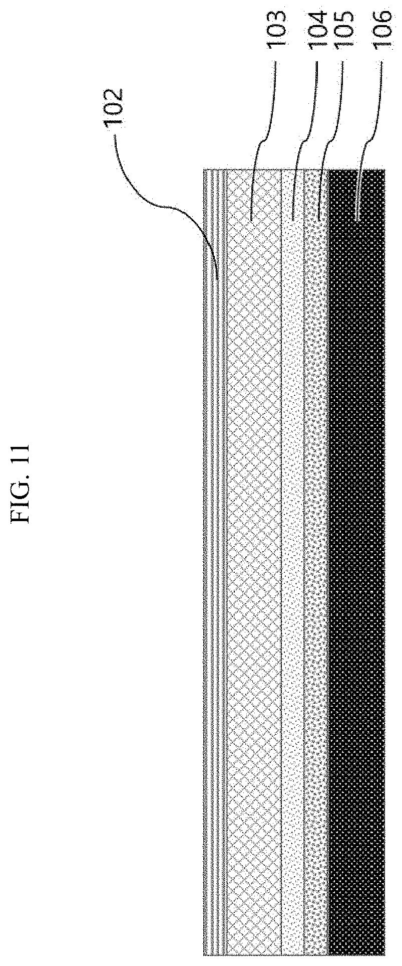
[0027] FIG. 11 illustrates an example of a film cross-section of a process of manufacturing a chip-on film type semiconductor package in which an adhesive layer 104 and a protective film layer 105 are laminated on one surface of the base material unit 103 of the printed circuit board layer 202 and a graphite layer 106 is laminated on one surface of the protective film layer 105 which faces the base material unit 103.
[0028] FIG. 12 illustrates an example of a cross-section of a chip-on film type semiconductor package in which a direction mounting element 109 is disposed on one surface of a circuit pattern layer 123 of a printed circuit board layer 202, a filling material 100 is filled in an empty space, and then an integrated circuit chip 101 is laminated on a film on which an adhesive layer 104 and a graphite layer 106 are sequentially laminated on one surface of a base material unit 103 of the printed circuit board layer 202 of FIG. 8.
[0029] FIG. 13 illustrates an example of a cross-section of a chip-on film type semiconductor package in which a direction mounting element 109 is disposed on one surface of a circuit pattern layer 123 of a printed circuit board layer 202, a filling material 100 is filled in an empty space, and then an integrated circuit chip 101 is laminated on a film on which a graphite layer 106 is laminated on one surface of a base material unit 103 of the printed circuit board layer 202 of FIG. 9.
[0030] FIG. 14 illustrates an example of a cross-section of a chip-on film type semiconductor package in which a direction mounting element 109 is disposed on one surface of a circuit pattern layer 123 of a printed circuit board layer 202, a filling material 100 is filled in an empty space, and then an integrated circuit chip 101 is laminated on a film on which an adhesive layer 104 and a graphite layer 106 are sequentially laminated on one surface of a base material unit 103 of the printed circuit board layer 202 of FIG. 10 and an adhesive layer 107 and a protective film layer 108 are sequentially laminated on one surface of the graphite layer 106 which is opposite to the base material unit 103.
[0031] FIG. 15 illustrates an example of a cross-section of a chip-on film type semiconductor package in which a direction mounting element 109 is disposed on one surface of a circuit pattern layer 123 of a printed circuit board layer 202, a filling material 100 is filled in an empty space, and then an integrated circuit chip 101 is laminated on a film on which an adhesive layer 104 and a protective film layer 105 are laminated on one surface of a base material unit 103 of the printed circuit board layer 202 of FIG. 11 and a graphite layer 106 is laminated on one surface of the protective film layer 105 which faces the base material unit 103.
[0032] FIG. 16 illustrates a chip-on film type semiconductor package with a structure in which an integrated circuit chip 101 connected to one surface of a printed circuit board layer 202 directly or by means of a mounting element 109 and an outer lead bonder pad 204 are disposed to be parallel to a length direction of the integrated circuit as a plan view in an upper direction.
[0033] FIG. 17 illustrates a chip-on film type semiconductor package with a structure in which the outer lead bonder pad 204 is disposed to be parallel to a length direction of an integrated circuit chip 101 and the graphite layer 106 is laminated in an area excluding an opposite surface of the area of the printed circuit board layer 202 on which the outer lead bonder pad is disposed as a plan view in a lower direction in which the graphite layer is laminated.
[0034] FIG. 18 illustrates a chip-on film type semiconductor package with a structure in which the outer lead bonder pad 204 is disposed to be parallel to a length direction of an integrated circuit chip 101 and the graphite layers 106 are laminated to be spaced apart from each other in an area excluding an opposite surface of the area of the printed circuit board layer 202 on which the outer lead bonder pad is disposed as a plan view in a lower direction in which the graphite layer is laminated.
DESCRIPTION OF MAIN REFERENCE NUMERALS OF DRAWINGS
[0035] 101: Driver integrated circuit chip
[0036] 102: Circuit pattern layer of printed circuit film layer
[0037] 103: Base material layer of printed circuit film layer
[0038] 104, 107: Adhesive layer
[0039] 105, 108: Protective film layer
[0040] 106: Graphite layer
[0041] 109: Bump for electrically connecting driver integrated circuit chip and printed circuit film
[0042] 110: Filler
[0043] 202: Printed circuit film layer
[0044] 301: Roller
[0045] 302: Graphite powder
[0046] 401: Graphite film
BEST MODE
[0047] Hereinafter, exemplary embodiments of a chip-on film type semiconductor package according to the present invention and a manufacturing method thereof will be described in detail with reference to the accompanying drawings to be easily carried out by those skilled in the art.
[0048] Hereinafter, a chip-on film type semiconductor package according to the present invention and a manufacturing method thereof will be described with reference to the accompanying drawings.
[0049] Hereinafter, a configuration and characteristics of the present invention will be described by way of exemplary embodiments, which are not intended to be limiting, but merely illustrative of the invention.
[0050] Hereinafter, a structure of a chip-on film type semiconductor package will be described with reference to FIG. 1.
[0051] A chip-on film type semiconductor package according to the present invention includes an integrated circuit chip 101, a printed circuit board layer 202, an outer lead bonder pad 204, and a graphite layer 106.
[0052] The integrated circuit chip 101 is connected to one surface of the printed circuit board layer 202 directly or by means of a mounting element 109. As long as the mounting element 109 electrically connects a circuit of the printed circuit board layer 202 and the integrated circuit chip 101, the mounting element is not limited. However, specifically, the mounting element 109 may be a bump and a material may be gold, copper, nickel, or a combination thereof.
[0053] In one embodiment of the present invention, the printed circuit board layer 202 may include a circuit pattern layer 102 and a base material unit 103. The circuit pattern layer 102 may be a pattern which configures an electrical circuit with the integrated circuit chip 101 and the material is not limited as long as a material configures a circuit. However, the material may be gold, copper, nickel, or a combination thereof. If the base material unit 103 is an insulating material, the material is not limited. However, the base material unit may be a flexible film or a transparent film having a visible plate to surface structure. Specifically, the base material unit may be a polyimide film.
[0054] In one embodiment of the present invention, a thickness of the printed circuit board layer 202 may be 25 .mu.m to 50 .mu.m. If the thickness is less than 25 .mu.m, the strength against the bending or tearing is degraded and if the thickness is more than 50 .mu.m, the flexibility is degraded so that the bending property may be deteriorated.
[0055] In one embodiment of the present invention, an exposed area of the mounting element 109 between the integrated circuit chip 101 and the printed circuit board layer 202 may be filled with a filler 110. As long as the filler 110 suppresses the oxidation of the mounting element 109 due to exposure to the air, the filler is not limited, but specifically, may be a liquid resin.
[0056] FIG. 2 illustrates a structure in which an integrated circuit chip 101 is connected to one surface of a printed circuit board layer 202 directly or by means of a mounting element 109 as a plan view in an upper direction of a chip-on film type semiconductor package.
[0057] In one embodiment of the present invention, the integrated circuit chip 101 may be a display driver integrated circuit chip (DDI chip).
[0058] The graphite layer 106 may be laminated on an opposite surface of the printed circuit board layer 202.
[0059] FIG. 3 illustrates a plan view of a lower direction of a chip-on film type semiconductor package in which a graphite layer is laminated.
[0060] In one embodiment of the present invention, the graphite layer 106 may be a carbonized polymer film or a film formed of graphite powder.
[0061] FIG. 4 illustrates a general printed circuit board layer 202 including a circuit pattern layer 102 formed on one surface of the base material unit 103.
[0062] FIG. 5 illustrates a process of laminating a graphite layer 106 on one surface of a printed circuit board layer 202 by disposing graphite powder 302 on an adhesive layer 104 on one surface of the base material unit 103 of the printed circuit board layer 202 of FIG. 4 and then pressurizing the graphite powder in both directions of a circuit pattern layer 102 and a base material unit 103 with a roller 301.
[0063] FIG. 6 illustrates a process of laminating a graphite layer 106 on one surface of a printed circuit board layer 202 by disposing a graphite film 401 on an adhesive layer 104 on one surface of the base material unit 103 of the printed circuit board layer 202 of FIG. 4 and then pressurizing the graphite film in both directions of a circuit pattern layer 102 and a base material unit 103 with a roller 301.
[0064] In one embodiment of the present invention, the graphite film 401 may be an artificial graphite, and specifically, a carbonized polymer film.
[0065] In one embodiment of the present invention, the polymer film may be a polyimide film.
[0066] In one embodiment of the present invention, the carbonization is to perform a heat treatment method including a carbonizing step and a graphite step.
[0067] In one embodiment of the present invention, the carbonizing step includes a step of carbonizing the polymer film to be converted into a carbonaceous film by introducing a polyimide film into a first heater with a first temperature interval.
[0068] In one embodiment of the present invention, the first temperature interval is an interval in which the temperature sequentially rises to 500.+-.50.degree. C. to 1,000.degree. C.
[0069] In one embodiment of the present invention, the graphite step includes a step of converting the carbonaceous film into a graphite film by introducing the carbonaceous film into a second heater having a second temperature interval in which the temperature linearly rises.
[0070] In one embodiment of the present invention, the second heater has a length of 4,000 mm to 6,000 mm
[0071] In one embodiment of the present invention, the second temperature interval is an interval in which the temperature sequentially rises to 1,000.degree. C. to 2,800.degree. C.
[0072] In one embodiment of the present invention, the second temperature interval may include a second-first temperature interval of 1,000.degree. C. to 1,500.degree. C., a second-second temperature interval of 1,500.degree. C. to 2,200.degree. C., and a second-third temperature interval of 2,200.degree. C. to 2,800.degree. C.
[0073] In one embodiment of the present invention, the graphite step includes a step of moving the carbonaceous film in a transverse direction at 0.33 mm/sec to 1.33 mm/sec in the second-first temperature interval and performing a thermal treatment on the carbonaceous film for one to four hours while rising an internal temperature of the second heater to 1.degree. C. to 5.degree. C. per minute.
[0074] In one embodiment of the present invention, a thickness of the graphite layer 106 may be 5 .mu.m to 40 .mu.m.
[0075] In one embodiment of the present invention, adhesive layers 104 and 107 may be further provided between the graphite layer 106 and the printed circuit board layer 202.
[0076] In one embodiment, the adhesive layers 104 and 107 may be pressure sensitive adhesives (PSA) which show or enhance an adhesive activity when a pressure is applied and specifically, may be acrylic adhesives or polyimide, polyethylene terephthalate double-sided tapes.
[0077] In one embodiment of the present invention, the adhesive layers 104 and 107 may include conductive particles.
[0078] In one embodiment of the present invention, a thickness of the adhesive layers 104 and 107 may be 3.5 .mu.m to 5 .mu.m.
[0079] FIG. 7 illustrates an example of a film cross-section of a process of manufacturing a chip-on film type semiconductor package in which a graphite layer 106 is laminated on one surface of the base material unit 103 of the printed circuit board layer 202.
[0080] FIG. 8 illustrates an example of a film cross-section of a process of manufacturing a chip-on film type semiconductor package in which an adhesive layer 104 and a graphite layer 106 are sequentially laminated on one surface of the base material unit 103 of the printed circuit board layer 202.
[0081] In one embodiment of the present invention, a protective film layer 108 may be further provided on one surface of the graphite layer 106.
[0082] In one embodiment of the present invention, the protective film layer 108 may be laminated on one surface of the graphite layer 106 which faces the base material unit 103 of the printed circuit board layer 202.
[0083] In one embodiment of the present invention, the protective film layer 108 may be an insulating film, and specifically, may be a polyester-based resin film and may include polyethylene terephthalate (PET), polybutylene terephthalate (PBT), polytrimethylene terephthalate (PTET), polycyclohexylene terephthalate (PCHT) and polyethylene naphthalate (PEN), or a combination thereof.
[0084] In one embodiment of the present invention, a thickness of the protective film layer 108 may be 1.5 .mu.m to 3.0 .mu.m.
[0085] FIG. 9 illustrates an example of a film cross-section of a process of manufacturing a chip-on film type semiconductor package in which a graphite layer 106 is laminated on one surface of the base material unit 103 of the printed circuit board layer 202 and an adhesive layer 107 and a protective film layer 108 are sequentially laminated on one surface of the graphite layer 106 which is opposite to the base material unit 103.
[0086] FIG. 10 illustrates an example of a film cross-section of a process of manufacturing a chip-on film type semiconductor package in which an adhesive layer 104 and a graphite layer 106 are sequentially laminated on one surface of the base material unit 103 of the printed circuit board layer 202 and an adhesive layer 107 and a protective film layer 108 are sequentially laminated on one surface of the graphite layer 106 which is opposite to the base material unit 103.
[0087] In one embodiment of the present invention, the protective film layer 108 may be laminated on one surface of the graphite layer 106 which is opposite to the base material unit 103 of the printed circuit board layer 202.
[0088] FIG. 11 illustrates an example of a film cross-section of a process of manufacturing a chip-on film type semiconductor package in which an adhesive layer 104 and a protective film layer 105 are laminated on one surface of the base material unit 103 of the printed circuit board layer 202 and a graphite layer 106 is laminated on one surface of the protective film layer 105 which faces the base material unit 103.
[0089] FIG. 1 illustrates an example of a cross-section of a chip-on film type semiconductor package in which a direction mounting element 109 is disposed on one surface of a circuit pattern layer 123 of a printed circuit board layer 202, a filling material 100 is filled in an empty space, and then an integrated circuit chip 101 is laminated on a film on which a graphite layer 106 is laminated on one surface of a base material unit 103 of the printed circuit board layer 202 of FIG. 7.
[0090] FIG. 12 illustrates an example of a cross-section of a chip-on film type semiconductor package in which a direction mounting element 109 is disposed on one surface of a circuit pattern layer 123 of a printed circuit board layer 202, a filling material 100 is filled in an empty space, and then an integrated circuit chip 101 is laminated on a film on which an adhesive layer 104 and a graphite layer 106 are sequentially laminated on one surface of a base material unit 103 of the printed circuit board layer 202 of FIG. 8.
[0091] FIG. 13 illustrates an example of a cross-section of a chip-on film type semiconductor package in which a direction mounting element 109 is disposed on one surface of a circuit pattern layer 123 of a printed circuit board layer 202, a filling material 100 is filled in an empty space, and then an integrated circuit chip 101 is laminated on a film on which a graphite layer 106 is laminated on one surface of a base material unit 103 of the printed circuit board layer 202 of FIG. 9.
[0092] FIG. 14 illustrates an example of a cross-section of a chip-on film type semiconductor package in which a direction mounting element 109 is disposed on one surface of a circuit pattern layer 123 of a printed circuit board layer 202, a filling material 100 is filled in an empty space, and then an integrated circuit chip 101 is laminated on a film on which an adhesive layer 104 and a graphite layer 106 are sequentially laminated on one surface of a base material unit 103 of the printed circuit board layer 202 of FIG. 10 and an adhesive layer 107 and a protective film layer 108 are sequentially laminated on one surface of the graphite layer 106 which is opposite to the base material unit 103.
[0093] In one embodiment of the present invention, the protective film layer 108 may be laminated on one surface of the graphite layer 106 which is opposite to the base material unit 103 of the printed circuit board layer 202.
[0094] FIG. 15 illustrates an example of a cross-section of a chip-on film type semiconductor package in which a direction mounting element 109 is disposed on one surface of a circuit pattern layer 123 of a printed circuit board layer 202, a filling material 100 is filled in an empty space, and then an integrated circuit chip 101 is laminated on a film on which an adhesive layer 104 and a protective film layer 105 are laminated on one surface of a base material unit 103 of the printed circuit board layer 202 of FIG. 11 and a graphite layer 106 is laminated on one surface of the protective film layer 105 which faces the base material unit 103.
[0095] The outer lead bonder pad 204 is located on one surface of the printed circuit board layer.
[0096] As long as the outer lead bonder pad 204 electrically connects a circuit of the printed circuit board layer 202 and a display panel, the outer lead bonder pad is not limited and a material thereof may be gold, copper, nickel, or a combination thereof.
[0097] In one embodiment of the present invention, the outer lead bonder pad 204 may be disposed to be parallel to a length direction of the integrated circuit.
[0098] FIG. 16 illustrates a chip-on film type semiconductor package with a structure in which an integrated circuit chip 101 connected to one surface of a printed circuit board layer 202 directly or by means of a mounting element 109 and an outer lead bonder pad 204 are disposed to be parallel to a length direction of the integrated circuit as a plan view in an upper direction.
[0099] In one embodiment of the present invention, the graphite layer 106 may be laminated in an area excluding an opposite surface of an area of the printed circuit board layer 202 in which the outer lead bonder pad is disposed. In the chip-on film type semiconductor package with this structure, a visibility of the outer lead bonder pad 204 disposed on the printed circuit board layer 202 in a direction in which the graphite layer 203 is laminated is improved so that the outer lead bonder pad 204 is visibly identified in the direction of the graphite layer 203 with naked eyes. Therefore, the visibility is improved and a bonding precision and a bonding strength during the outer lead bonding process (OLB process) are improved.
[0100] FIG. 17 illustrates a chip-on film type semiconductor package with a structure in which the outer lead bonder pad 204 is disposed to be parallel to a length direction of an integrated circuit chip 101 and the graphite layers 106 is laminated in an area excluding an opposite surface of the area of the printed circuit board layer 202 on which the outer lead bonder pad is disposed as a plan view in a lower direction in which the graphite layer is laminated.
[0101] In one embodiment of the present invention, two or more graphite layers 106 may be laminated to be spaced apart from each other. In this case, individual unit sections of the integrated circuit chip are divided even in the direction of the graphite layer 203 so that a bonding precision and a bonding strength during the outer lead bonding process (OLB process) are improved.
[0102] FIG. 18 illustrates a chip-on film type semiconductor package with a structure in which the outer lead bonder pad 204 is disposed to be parallel to a length direction of an integrated circuit chip 101 and the graphite layers 106 are laminated to be spaced apart from each other in an area excluding an opposite surface of the area of the printed circuit board layer 202 on which the outer lead bonder pad is disposed as a plan view in a lower direction in which the graphite layer is laminated.
[0103] In one embodiment of the present invention, the integrated circuit chip 101 may be disposed to be parallel to a length direction of the printed circuit board layer 202. In this case, even though a structure in which the graphite layer 106 is laminated in an area excluding an opposite surface of an area of the printed circuit board layer 202 on which the outer lead bonder pad is disposed is employed to visibly identify the outer lead bonder pad 204 with naked eyes even in the direction of the graphite layer 106, a continuous pressurizing process on the printed circuit board layer 202 by a roll to roll/reel process to reel is possible when the graphite layer 106 is laminated to improve the workability while improving the visibility, the bonding precision, and the bonding strength.
[0104] In one embodiment of the present invention, in a state in which the printed circuit board layer 202 and the graphite layer 106 are wound on a roll in the form of a film, both surfaces are pressurized by two rollers 301 to be primarily laminated by a roll to roll/reel to reel process. In this case, a pressure of the roller may be 3 to 3 kg. Further, a carrier film may be supplied on one surface of the graphite layer 106 by a roll to roll process to be laminated and a primarily laminated film may be laminated in the order of the printed circuit board layer 202/the graphite layer 106/the carrier film layer (not illustrated) or the printed circuit board layer 202/the adhesive layer 104/the graphite layer 106/the carrier film layer (not illustrated).
[0105] In one embodiment of the present invention, in a state in which the primarily laminated film and the adhesive layers 104 and 107 are wound on a roll in the form of a film, both surfaces may be pressurized to be secondarily laminated by the roll to roll/reel to reel process. In this case, a pressure of the roller may be 3 to 20 kg. Further, a release film may be supplied on one surface of the graphite layer 106 by a roll to roll process to be laminated and a secondarily laminated film may be laminated in the order of the printed circuit board layer 202/the adhesive layer 104/the graphite layer 106/the adhesive layer 107/the release film layer (not illustrated) or the printed circuit board layer 202/the adhesive layer 107/the graphite layer 106/the release film layer (not illustrated).
[0106] In one embodiment of the present invention, in a state in which the secondarily laminated film and the protective film layers 105 and 108 are wound on a roll in the form of a film, both surfaces are pressurized to be secondarily laminated by the roll to roll/reel to reel process. In this case, the pressure of the roller may be 3 to 20 kg and a temperature of the roller may be 70 to 90.degree. C. Further, a tertiary laminated film may be laminated in order of the printed circuit board layer 202/the adhesive layer 104/the graphite layer 106/the adhesive layer 107/the protective film layer 108 or the printed circuit board layer 202/the adhesive layer 107/the graphite layer 106/the protective film layer 108.
[0107] Hereinafter, a display device including the above described chip-on film type semiconductor package, a substrate, and a display panel will be described.
[0108] In one embodiment of the present invention, the substrate may be electrically connected to an outer lead bonder pad 204 of the chip-on film type semiconductor package.
[0109] In one embodiment of the present invention, the substrate may further include an outer lead bonder pad (not illustrated) and may be electrically connected to the outer lead bonder pad 204 of the chip-on film type semiconductor package.
[0110] In one embodiment of the present invention, the substrate may further include an outer lead bonder pad (not illustrated) and may be electrically connected to the outer lead bonder pad 204 of the chip-on film type semiconductor package. In this case, an anisotropic conductive film (ACF) layer may be further provided between the outer lead bonder pad (not illustrated) of the substrate and the outer lead bonder pad 204 of the chip-on film type semiconductor package. The outer lead bonder pad (not illustrated) of the substrate/the anisotropic conductive film layer/the outer lead bonder pad 204 of the chip-on film type semiconductor package are sequentially disposed and then laminated by an outer lead bonding process (OLB process).
[0111] In one embodiment of the present invention, the display panel may be a liquid crystal display or a light emitting diode display and a configuration module may include a module of a display panel which is generally used.
[0112] The chip-on film type semiconductor package is electrically connected to the substrate and the display panel to control a corresponding pixel of the display panel, in accordance with a driving signal of the integrated circuit chip, to be driven by an electrical signal.
[0113] The above description should be construed as examples of embodiments rather than limiting the scope of the invention. Therefore, the invention is not determined by the described matters, but may be determined by the claims and equivalents to the claims.
* * * * *
D00000
D00001
D00002
D00003
D00004
D00005
D00006
D00007
D00008
D00009
D00010
D00011
D00012

D00013

D00014

D00015

D00016

D00017

D00018

XML
uspto.report is an independent third-party trademark research tool that is not affiliated, endorsed, or sponsored by the United States Patent and Trademark Office (USPTO) or any other governmental organization. The information provided by uspto.report is based on publicly available data at the time of writing and is intended for informational purposes only.
While we strive to provide accurate and up-to-date information, we do not guarantee the accuracy, completeness, reliability, or suitability of the information displayed on this site. The use of this site is at your own risk. Any reliance you place on such information is therefore strictly at your own risk.
All official trademark data, including owner information, should be verified by visiting the official USPTO website at www.uspto.gov. This site is not intended to replace professional legal advice and should not be used as a substitute for consulting with a legal professional who is knowledgeable about trademark law.