Tomosynthesis With Shifting Focal Spot X-ray System Using An Addressable Array
SMITH; Andrew P. ; et al.
U.S. patent application number 16/095416 was filed with the patent office on 2020-11-12 for tomosynthesis with shifting focal spot x-ray system using an addressable array. This patent application is currently assigned to Hologic, Inc.. The applicant listed for this patent is HOLOGIC, INC.. Invention is credited to John LAVIOLA, Andrew P. SMITH.
| Application Number | 20200352531 16/095416 |
| Document ID | / |
| Family ID | 1000005033503 |
| Filed Date | 2020-11-12 |
View All Diagrams
| United States Patent Application | 20200352531 |
| Kind Code | A1 |
| SMITH; Andrew P. ; et al. | November 12, 2020 |
TOMOSYNTHESIS WITH SHIFTING FOCAL SPOT X-RAY SYSTEM USING AN ADDRESSABLE ARRAY
Abstract
A tomosynthesis system has an x-ray source with an addressable array of electron emitting sections on the cathode. The x-ray source moves rotationally about an imaging target, such as a breast. During the rotation, x-rays are emitting from the x-ray source while the x-ray source continues to move. During the emission of x-rays, different subsets of electron-emitting sections of the addressable array are activated to compensate for movement of the x-ray source. By activating the different subsets of electron-emitting sections, an effective focal spot of the x-ray position appears to retain the same shape, size, and position from the perspective of the imaging target, despite movement of the x-ray source itself.
| Inventors: | SMITH; Andrew P.; (Marlborough, MA) ; LAVIOLA; John; (Marlborough, MA) | ||||||||||
| Applicant: |
|
||||||||||
|---|---|---|---|---|---|---|---|---|---|---|---|
| Assignee: | Hologic, Inc. Marlborough MA |
||||||||||
| Family ID: | 1000005033503 | ||||||||||
| Appl. No.: | 16/095416 | ||||||||||
| Filed: | April 21, 2017 | ||||||||||
| PCT Filed: | April 21, 2017 | ||||||||||
| PCT NO: | PCT/US2017/028934 | ||||||||||
| 371 Date: | October 22, 2018 |
Related U.S. Patent Documents
| Application Number | Filing Date | Patent Number | ||
|---|---|---|---|---|
| 62326451 | Apr 22, 2016 | |||
| Current U.S. Class: | 1/1 |
| Current CPC Class: | H01J 2201/30469 20130101; H01J 35/065 20130101; A61B 6/502 20130101; H01J 35/10 20130101; A61B 6/4476 20130101; H01J 2235/068 20130101; A61B 6/4021 20130101; A61B 6/405 20130101; A61B 6/025 20130101 |
| International Class: | A61B 6/00 20060101 A61B006/00; A61B 6/02 20060101 A61B006/02; H01J 35/10 20060101 H01J035/10; H01J 35/06 20060101 H01J035/06 |
Claims
1. A system for radiographic imaging, the system comprising: a rotating arm configured to rotate relative to a target tissue; a radiation source attached to the rotating arm, the radiation source comprising a cathode and an anode, wherein the cathode comprises an array of electron-emitting sections; and a controller operatively connected to the cathode, the controller configured to activate a first subset of the array of electron-emitting sections when the radiation source is located in a first position relative to the target, and activate a second subset of the array of electron-emitting sections when the radiation source is located in a second position relative to the target.
2. The system of claim 1, wherein the rotating arm moves in a first direction and the second subset of the array of electron-emitting sections includes electron-emitting sections spaced apart from the first subset of the array of electron-emitting sections in a direction opposite the first direction.
3. The system of claim 1, wherein each electron-emitting section includes at least one field emission emitter.
4. The system of claim 3, wherein each electron-emitting section includes at least one carbon-nanotube emitter.
5. The system of claim 1, wherein the first subset of electron-emitting sections and the second subset of electron-emitting sections are individually addressable by the controller.
6. The system of claim 1, wherein the array comprises multiple rows of electron-emitting sections, wherein each row is individually addressable by the controller.
7. The system of claim 6, wherein each row includes a gate portion and an emitter portion, the gate portion connected to a transistor connected to the controller.
8. The system of claim 1, wherein each electron-emitting section is individually addressable by the controller.
9. The system of claim 8, wherein each electron-emitting section includes a gate portion and an emitter portion, the gate portion connected to a transistor connected to the controller.
10. The system of claim 1, wherein second subset of electron-emitting sections are selected to compensate for movement from the first position to the second position.
11. The system of claim 1, wherein the radiation source is configured to emit radiation to a single location on the target as the radiation source moves from the first position and the second position.
12. The system of claim 1, wherein the controller and the radiation source are configured to shift from the first subset of electron-emitting sections to the second subset of electron-emitting sections to maintain the single location as the radiation source moves from the first position and the second position.
13. A method for radiographic imaging, the method comprising: moving a radiation source relative to a target from a first position to a second position while emitting radiation from the radiation source to a location of the target, the radiation source including an array of electron-emitting sections; while moving the radiation source from the first position to the second position, activating a first subset of the electron-emitting sections at the first position and activating a second subset of electron-emitting sections at the second position; and detecting the emitted radiation.
14. The method of claim 13, wherein the second subset of the array of electron-emitting sections includes electron-emitting sections from the first subset of the array of electron-emitting sections.
15. The method of claim 13, wherein each electron-emitting section includes at least one field emission emitter.
16. The method of claim 13, wherein each electron-emitting section includes at least one carbon-nanotube emitter.
17. The method of claim 13, wherein the array comprises multiple rows of electron-emitting sections, wherein each row is individually addressable.
18. The method of claim 13, wherein each electron-emitting section is individually addressable.
19. The method of claim 13, further comprising selecting the second subset of electron-emitting sections to compensate for movement from the first position to the second position.
20. A method for radiographic imaging, the method comprising: activating a first subset of electron-emitting sections of a cathode of a radiation source; directing radiation emitted from the radiation source to a location on a target; moving the radiation source relative to the target; and while moving the radiation source, deactivating the first subset of the electron-emitting sections and activating a second subset of electron-emitting sections to maintain the location on the target.
21. The method of claim 20, wherein the second subset of electron-emitting sections includes electron-emitting sections from the first subset of electron-emitting sections.
22. The method of claim 20, wherein the cathode comprises multiple rows of electron-emitting sections, and each row is individually addressable.
23. The method of claim 20, wherein each electron-emitting section comprises a single emitter that is individually addressable.
24. A radiation source, for use in radiographic imaging, comprising a cathode including a three-dimensional addressable array having a plurality of addressable electron-emitting sections.
25. The radiation source of claim 24, wherein the three-dimensional addressable array comprises a plurality of a cathode plates.
26. The radiation source of claim 24, wherein the three-dimensional addressable array is a v-shaped three-dimensional array.
27. The radiation source of claim 24, wherein the three-dimensional addressable array is a pyramidal three-dimensional array.
Description
CROSS-REFERENCE TO RELATED APPLICATIONS
[0001] This application is being filed on 21 Apr. 2017, as a PCT international patent application, and claims priority to and the benefit of U.S. Provisional Application No. 62/326,451, filed on Apr. 22, 2016, which is incorporated herein by reference in its entirety.
BACKGROUND
[0002] Breast tomosynthesis is an imaging technology in which images of a stationary compressed breast are acquired at multiple angles during a short scan. The images are organized as a series of thin high-resolution image "slices" that can be displayed individually or in a dynamic cine mode. Breast tomosynthesis systems move the x-ray source to a variety of different imaging positions relative to an x-ray detector during image acquisition. Reconstructed tomosynthesis slices advantageously reduce or eliminate problems caused by tissue overlap and structure noise in two-dimensional mammography imaging. However, movement of the x-ray source introduces some technological complications.
[0003] Typical tomosynthesis systems are arranged to either smoothly and continuously traverse a path during an image scan or utilize stop-and-start scanning procedures. The x-ray source is activated for an exposure time of about 10 ms to 100 ms as the x-ray source moves into each of several imaging locations in the imaging path, and exposure is repeated with a cycle period of 200 ms to 2 seconds. After each exposure the x-ray source is deactivated. As the x-ray source moves between imaging locations the contents of the digital image detector are read out and stored. There is a minimum time period associated with reading the image from the digital detector, and the overall speed of the tomosynthesis scan is determined by the minimum time period for detector read, the exposure time at each location, and the number of exposures. For continuous scans, the x-ray source is moved through space during each exposure period in a tomosynthesis system, which may result in blurring that may reduce diagnostic accuracy.
SUMMARY
[0004] In one aspect, the technology relates to a system for radiographic imaging, the system having: a rotating arm configured to rotate relative to a target tissue; a radiation source attached to the rotating arm, the radiation source having a cathode and an anode, wherein the cathode includes an array of electron-emitting sections; and a controller operatively connected to the cathode, the controller configured to activate a first subset of the array of electron-emitting sections when the radiation source is located in a first position relative to the target, and activate a second subset of the array of electron-emitting sections when the radiation source is located in a second position relative to the target. In an embodiment, the rotating arm moves in a first direction and the second subset of the array of electron-emitting sections has electron-emitting sections spaced apart from the first subset of the array of electron-emitting sections in a direction opposite the first direction. In another embodiment, each electron-emitting section includes at least one field emission emitter. In yet another embodiment, each electron-emitting section includes at least one carbon-nanotube emitter. In still another embodiment, the first subset of electron-emitting sections and the second subset of electron-emitting sections are individually addressable by the controller.
[0005] In another embodiment of the above aspect, the array has multiple rows of electron-emitting sections, wherein each row is individually addressable by the controller. In an embodiment, each row includes a gate portion and an emitter portion, the gate portion connected to a transistor connected to the controller. In another embodiment, each electron-emitting section is individually addressable by the controller. In yet another embodiment, each electron-emitting section includes a gate portion and an emitter portion, the gate portion connected to a transistor connected to the controller. In still another embodiment, second subset of electron-emitting sections are selected to compensate for movement from the first position to the second position.
[0006] In another embodiment of the above aspect, the radiation source is configured to emit radiation to a single location on the target as the radiation source moves from the first position and the second position. In an embodiment, the controller and the radiation source are configured to shift from the first subset of electron-emitting sections to the second subset of electron-emitting sections to maintain the single location as the radiation source moves from the first position and the second position.
[0007] In another aspect, the technology relates to a method for radiographic imaging, the method including: moving a radiation source relative to a target from a first position to a second position while emitting radiation from the radiation source to a location of the target, the radiation source including an array of electron-emitting sections; while moving the radiation source from the first position to the second position, activating a first subset of the electron-emitting sections at the first position and activating a second subset of electron-emitting sections at the second position; and detecting the emitted radiation. In an embodiment, the second subset of the array of electron-emitting sections includes electron-emitting sections from the first subset of the array of electron-emitting sections. In another embodiment, each electron-emitting section includes at least one field emission emitter. In yet another embodiment, each electron-emitting section includes at least one carbon-nanotube emitter. In still another embodiment, the array has multiple rows of electron-emitting sections, wherein each row is individually addressable.
[0008] In another embodiment of the above aspect, each electron-emitting section is individually addressable. In an embodiment, the method includes selecting the second subset of electron-emitting sections to compensate for movement from the first position to the second position.
[0009] In another aspect, the technology relates to a method for radiographic imaging, the method including: activating a first subset of electron-emitting sections of a cathode of a radiation source; directing radiation emitted from the radiation source to a location on a target; moving the radiation source relative to the target; and while moving the radiation source, deactivating the first subset of the electron-emitting sections and activating a second subset of electron-emitting sections to maintain the location on the target. In an embodiment, the second subset of electron-emitting sections includes electron-emitting sections from the first subset of electron-emitting sections. In another embodiment, the cathode has multiple rows of electron-emitting sections, and each row is individually addressable. In yet another embodiment, each electron-emitting section includes a single emitter that is individually addressable.
[0010] In another aspect, the technology relates to a radiation source, for use in radiographic imaging, comprising a cathode including a three-dimensional addressable array having a plurality of addressable electron-emitting sections. In an embodiment, the three-dimensional addressable array comprises a plurality of a cathode plates. In another embodiment, the three-dimensional addressable array is a v-shaped three-dimensional array. In yet another embodiment, the three-dimensional addressable array is a pyramidal three-dimensional array.
[0011] This summary is provided to introduce a selection of concepts in a simplified form that are further described below in the Detailed Description. This summary is not intended to identify key features or essential features of the claimed subject matter, nor is it intended to be used to limit the scope of the claimed subject matter.
BRIEF DESCRIPTION OF THE DRAWINGS
[0012] FIG. 1A depicts a breast tomosynthesis system.
[0013] FIG. 1B depicts movement of an x-ray source in a breast tomosynthesis system.
[0014] FIG. 2A depicts an example x-ray source.
[0015] FIG. 2B depicts an anode having a first angle.
[0016] FIG. 2C depicts an anode having a second angle.
[0017] FIG. 2D depicts a cathode having an addressable array of electron-emitting sections.
[0018] FIG. 2E depicts a cathode having an addressable array of electron-emitting sections.
[0019] FIG. 2F depicts field-emission electron emitters on a cathode.
[0020] FIG. 2G depicts a portion of an addressable array of field-emission electron emitters on a cathode.
[0021] FIG. 2H depicts two cathode plates having addressable arrays of electron-emitting sections.
[0022] FIG. 2I depicts a side view of a v-shaped three-dimensional array.
[0023] FIG. 2J depicts a perspective view of the v-shaped three-dimensional array
[0024] FIG. 2K depicts a set of cathode plates having addressable arrays of electron-emitting sections.
[0025] FIG. 2L depicts a perspective view of a pyramidal three-dimensional addressable array.
[0026] FIG. 3A depicts movement of an x-ray source in a breast tomosynthesis system.
[0027] FIG. 3B depicts an example of activating electron-emitting sections during movement of the x-ray source.
[0028] FIG. 3C depicts an example of activating electron-emitting sections during movement of the x-ray source.
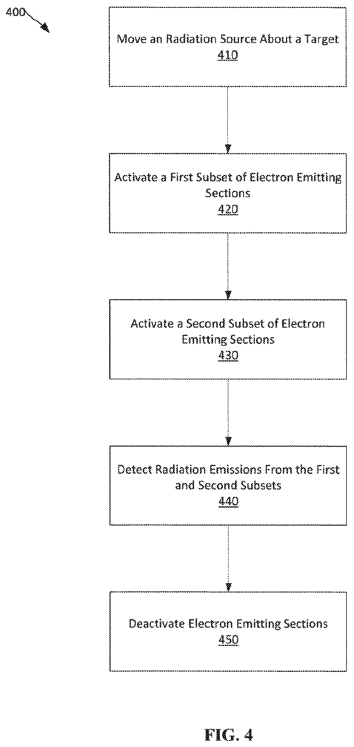
[0029] FIG. 4 depicts a method of using a tomosynthesis system for imaging.
[0030] FIG. 5 depicts illustrates one example of a suitable operating environment in which one or more of the present examples can be implemented.
[0031] FIG. 6 is an embodiment of a network in which the various systems and methods disclosed herein may operate.
DETAILED DESCRIPTION
[0032] The present technology relates to methods and systems suitable for imaging a target. One particular application for the present technology is for use in breast tomosynthesis. As discussed above, as an x-ray source moves relative to a target, such as a breast, x-rays are emitted from the x-ray source at various positions. In certain examples, the x-ray source does not stop moving during the x-ray emission. The continuous movement causes blurring in the resultant imagery as the detector receives x-rays from different origination locations during the exposure time. The present technology allows for the incident x-rays during exposure to originate from approximately the same location from the perspective of the imaging target (that is, from the perspective of the imaging target, an effective focal spot of the x-ray emission appears to stationary during the exposure time). To do so, a cathode having an addressable array of electron-emitting sections is utilized.
[0033] As discussed in further detail below, by activating different or various portions of the electron-emitting sections on the cathode, the location, size, and shape of electron emission from a cathode can be controlled. By controlling the location, size, and shape of the electron emission from the cathode, a focal spot on the anode is also altered, thus allowing for control of the focal spot on the anode. Through control of the focal spot on the anode, an effective focal spot remains constant from the perspective of the breast even during movement of the x-ray source during an exposure in relation to the breast. Maintaining a constant effective focal spot during an exposure from the perspective of the breast allows for more accurate and clear imaging, among other benefits.
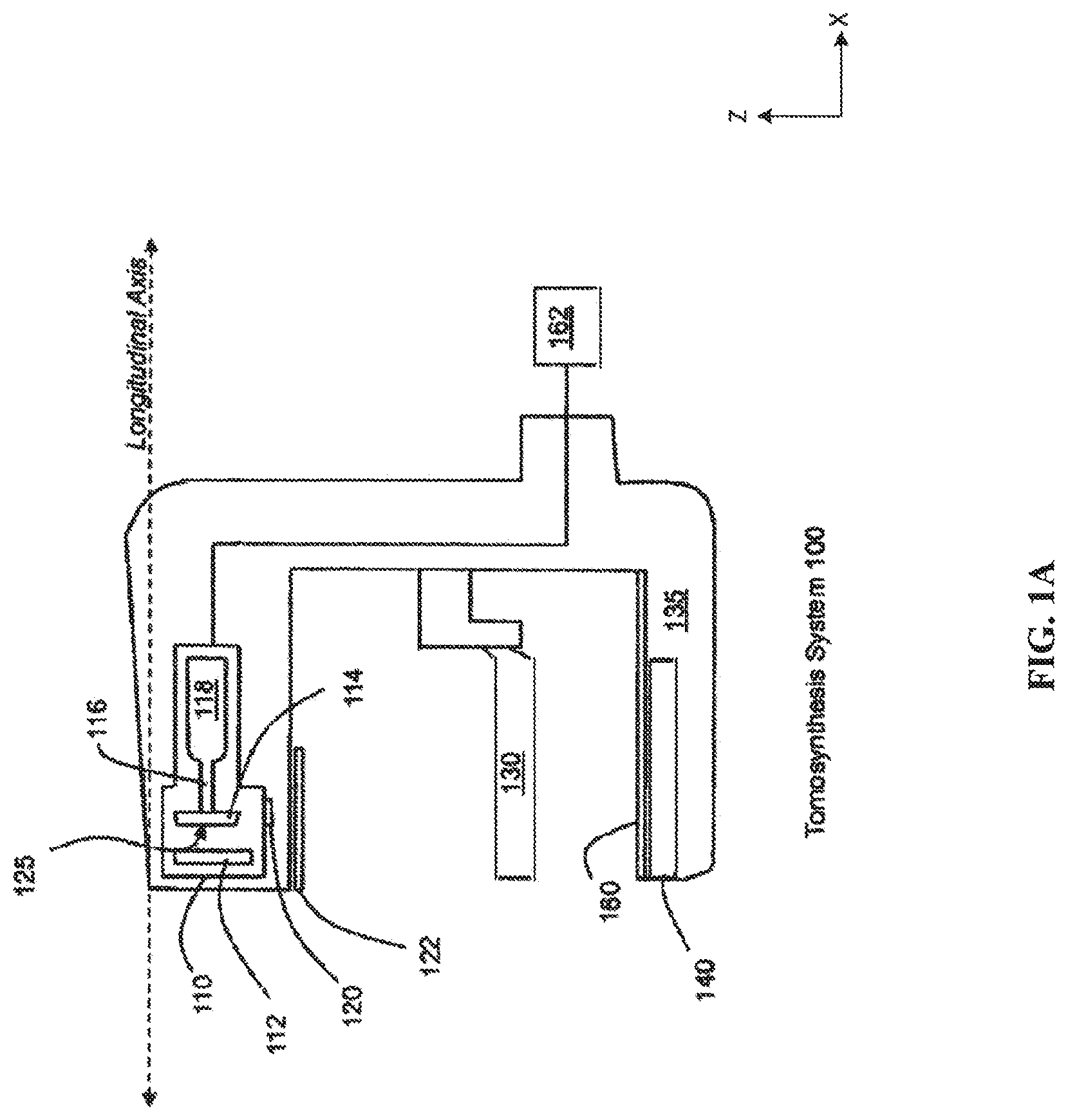
[0034] FIG. 1A depicts a breast tomosynthesis system 100. The tomosynthesis system 100 includes an x-ray tube 110, upper compression paddle 130, breast platform 135, an anti-scatter grid 160 and a detector 140. The x-ray source 110 includes a cathode 112, an anode 114 that is mounted on a shaft 116 and rotated by a motor 118, and a tube port 120. The x-ray source 110 is discussed below in further detail below with respect to FIGS. 2A-2G. The x-ray source 110 may also be operatively connected to a controller 162 for control of the x-ray source 110. A filter 122 may also be attached to the x-ray source or otherwise configured to filter the x-ray emission form the x-ray source 110.
[0035] The x-ray source 110 is attached to a rotating arm 105 that is configured to rotate about an axis parallel to the depicted longitudinal axis, both of which are parallel to the x-axis as shown in FIG. 1A. The rotating arm may be further connected to the controller 162 for control of the rotating arm and the x-ray source 110. During operation of the tomosynthesis system 100, a breast is held in place by the upper and lower compression paddles 130, 135 while radiation is being emitted from the x-ray source 110. The detector 140 may be stationary or may move during x-ray emission.
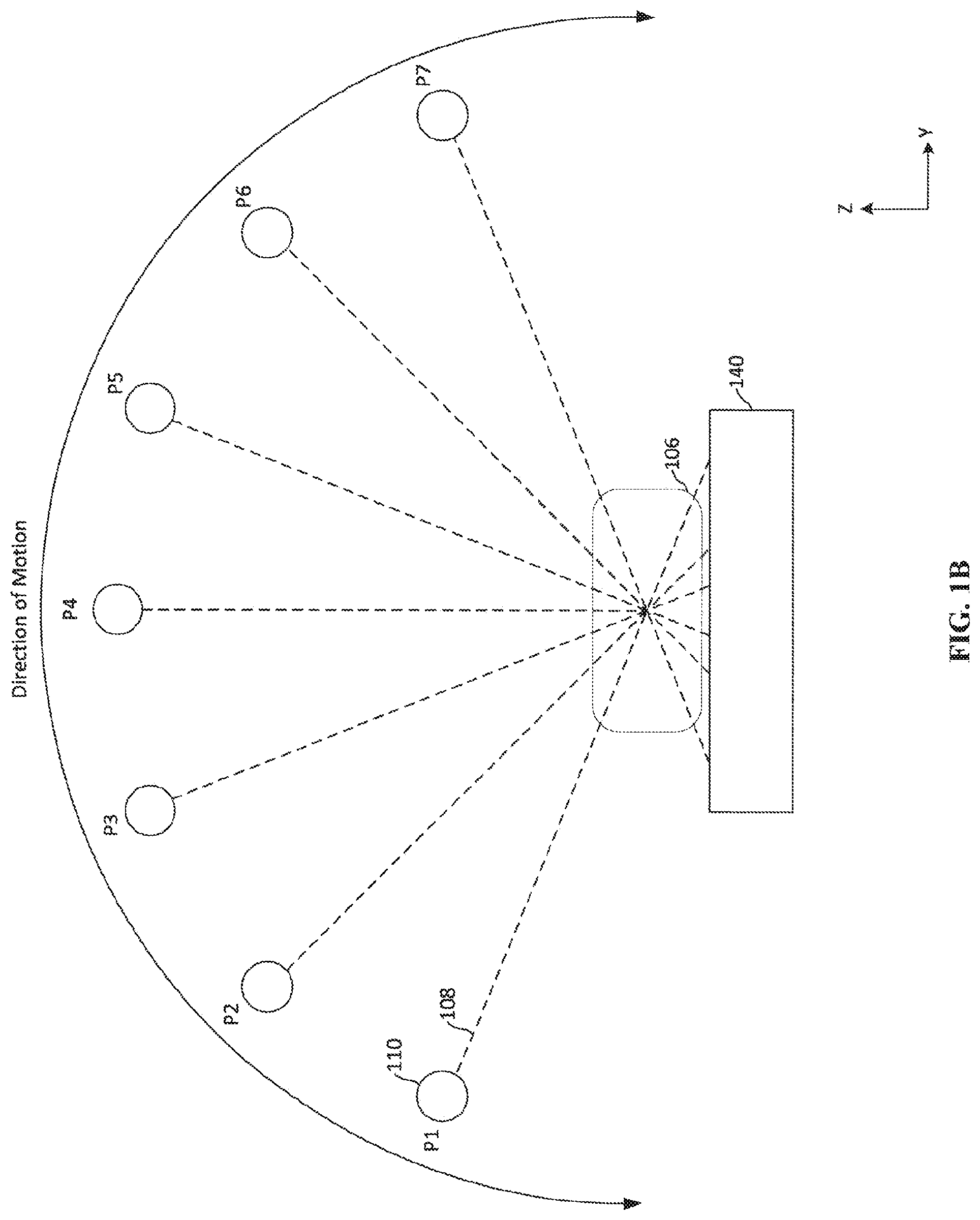
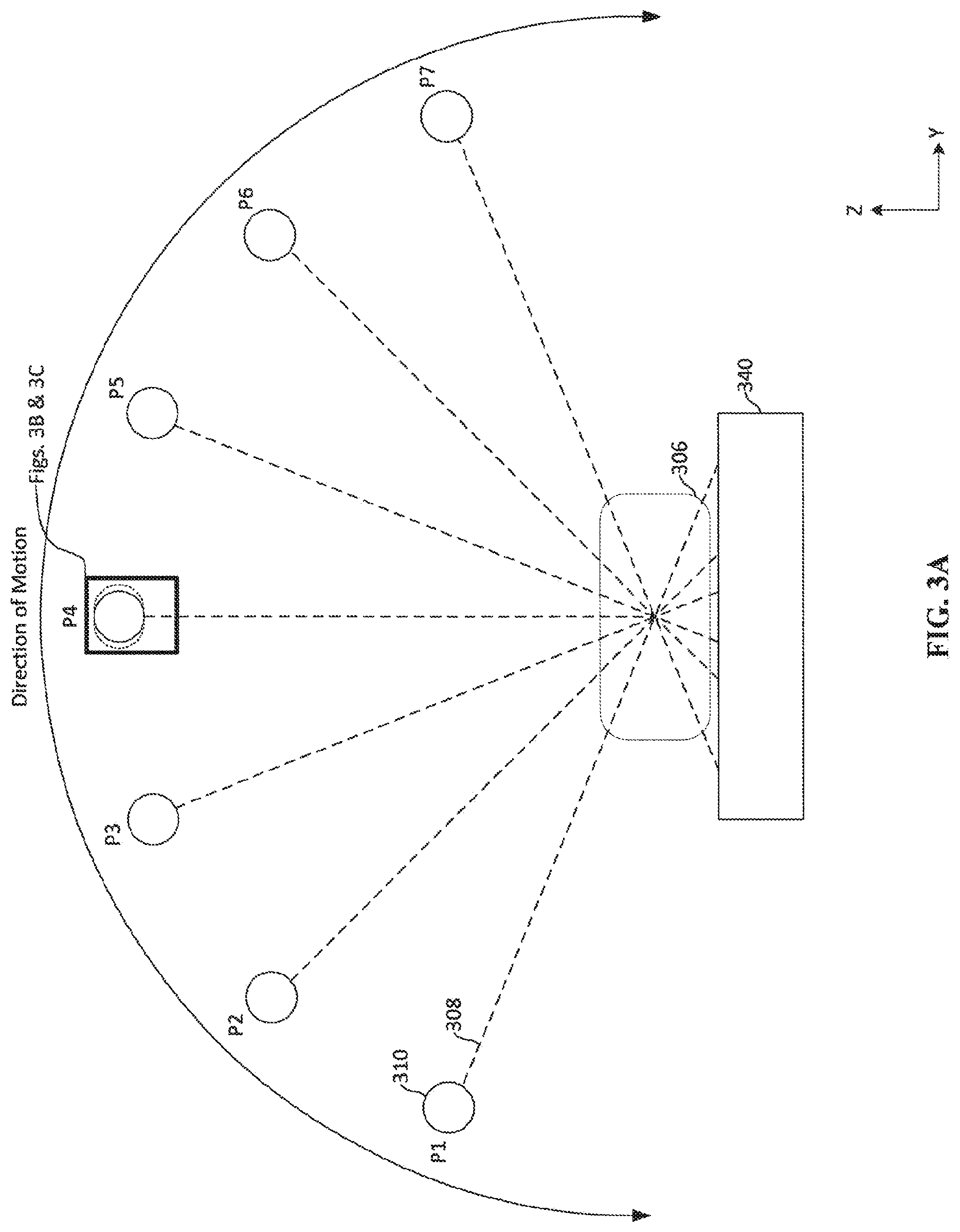
[0036] FIG. 1B depicts movement of an x-ray source 110 in the breast tomosynthesis system 100. Once the breast 106 is fixed in between the upper and lower compression paddles 130, 135, the rotating arm 105 rotates about the breast and the x-ray source 110 emits an x-ray emission 110 at multiple relative positions P1-P7 on an arc during the rotation, as shown in FIG. 1B. In examples the arc may span anywhere from 5 degrees to 360 degrees about the target (with 0 degrees and 360 degrees representing a horizontal line). In some applications, the arc spans between 15 degrees and 270 degrees. The arc length between positions may also be smaller or larger than depicted in FIG. 1B. That is, if the same number of positions are utilized on arcs having a total angle of 360 degrees and 135 degrees, the spacing between the positions in the 135 degree arc will be smaller. The motion of the x-ray source 110 is shown exaggerated for illustrative purposes. That is, during a tomosynthesis imaging procedure, the x-ray source 110 need not move across the complete range of motion depicted. In examples, the emissions may only occur between positions P1 and P4, or between positions P3 and P6, and so on. As noted above, the depicted positions P1 and P7 are relative positions that approximate locations where emission occurs for reference purposes only. For example, when the x-ray source reaches a position, such as P4, the x-ray source will begin emitting an x-ray emission 108 towards the breast 106. The x-ray emission 108 passes through the breast before reaching the detector 140. The emission of x-rays from the x-ray source 110 may be for a period of approximately 10 ms to 100 ms. During that period of emission, the x-ray source 110 continues to move relative to the compressed breast 106 and the detector 140. In traditional systems, blurring occurs due to the continuous movement during emission. In the present technology, however, the x-ray emission 108 can be altered during the movement to allow for the x-ray emission 108, as discussed further below. While only seven positions P1-P7 are shown in FIG. 1B, a greater or few number of positions may be utilized depending on the particular application.
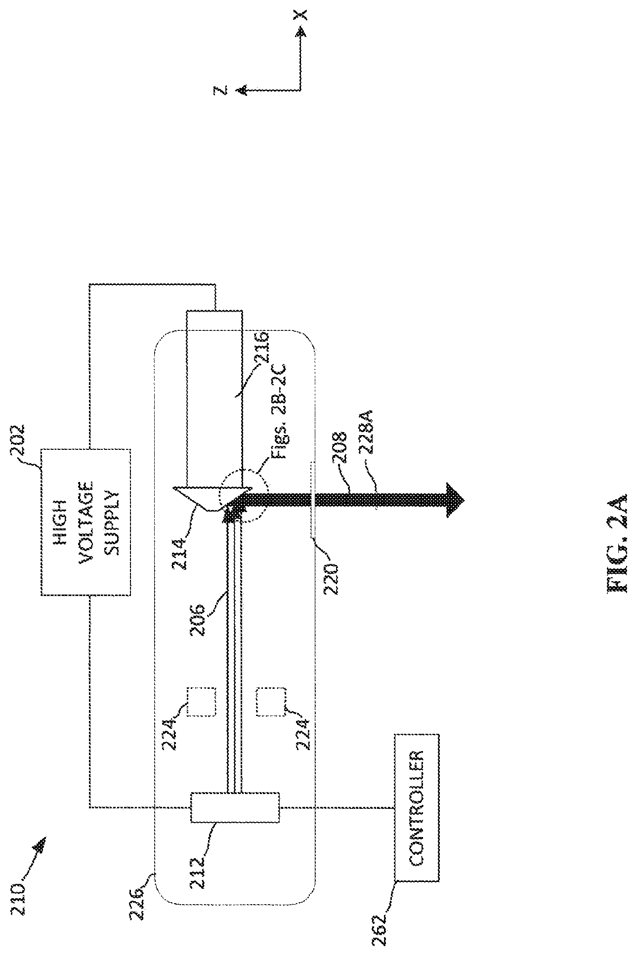
[0037] FIG. 2A depicts a simplified example x-ray source 210. The example x-ray source 210 as shown includes a vacuum tube 226 housing a cathode 212 and an anode 214. The anode 214 may be attached to a shaft 216 and a motor (not shown) to allow for the anode 214 to be rotated during operation to prevent overheating of a target location on the anode 214. The cathode 212 and the anode 214 are also attached to high voltage power supply 202. The cathode 212 is connected to a controller 262 for control of the cathode 212 activation.
[0038] When the cathode 212 is activated, electrons are emitted from the cathode 212. A high voltage difference between the cathode 212 and the anode 214 causes the electrons to accelerate towards the anode 214 as an electron beam 206. Upon colliding and interacting with the anode 214, the electrons cause an x-rays to be emitted from the anode 214 in all directions. Some of the x-rays are emitted through the tube port 220, as indicated by x-ray emission 208, towards the imaging target, such as a breast. Optionally, the electrons may be focused to a particular spot on the anode 214 by a focusing device 224. The particular spot where electrons strike the anode 214 is referred to herein as the anode focal spot. The anode focal spot is represented by a two-dimensional area on the surface of the anode 214.
[0039] The size and location of the anode focal spot can be altered by focusing the electron beam 206 with a focusing device 224. The focusing device 224 may be a focus ring or focus cup that generates an electric or magnetic field that alters the direction of the electron beam 206 as it passes through or by the focusing device 224. In such an example, the focusing device is able to deflect the electron beam in both the y-direction and the z-direction, as shown in FIG. 2A. By deflecting the electron beam 206 in two-dimensions, the electron beam 206 can be focused to a smaller anode focal spot. For instance, if the cathode 212 emits electrons from a 3 mm.times.3 mm area, the focus-ring focusing device 224 may focus the electron beam 206 to a 0.3 mm.times.0.3 mm anode focal spot. In another example, the focusing device 224 may comprise two elements located on opposite sides of the electron beam 206. The two elements are capable of deflecting the electron beam in a single direction, such as the y-direction, by generating an electric or magnetic field. In such an example, if the cathode 212 emits electrons from a 3 mm.times.3 mm area, the two-element focusing device 224 may focus the electron beam 206 to a 0.3 mm.times.3 mm anode focal spot. The 3 mm dimension may then be shortened from the angle of the anode, as discussed below. Focusing devices may be arranged or configured to focus any size or shape of an electron beam coming from the cathode 212. The x-ray emission 208 generated from the anode focal spot in the direction of the breast through the tube port also defines a spot, referred to as an effective focal spot and discussed further below.
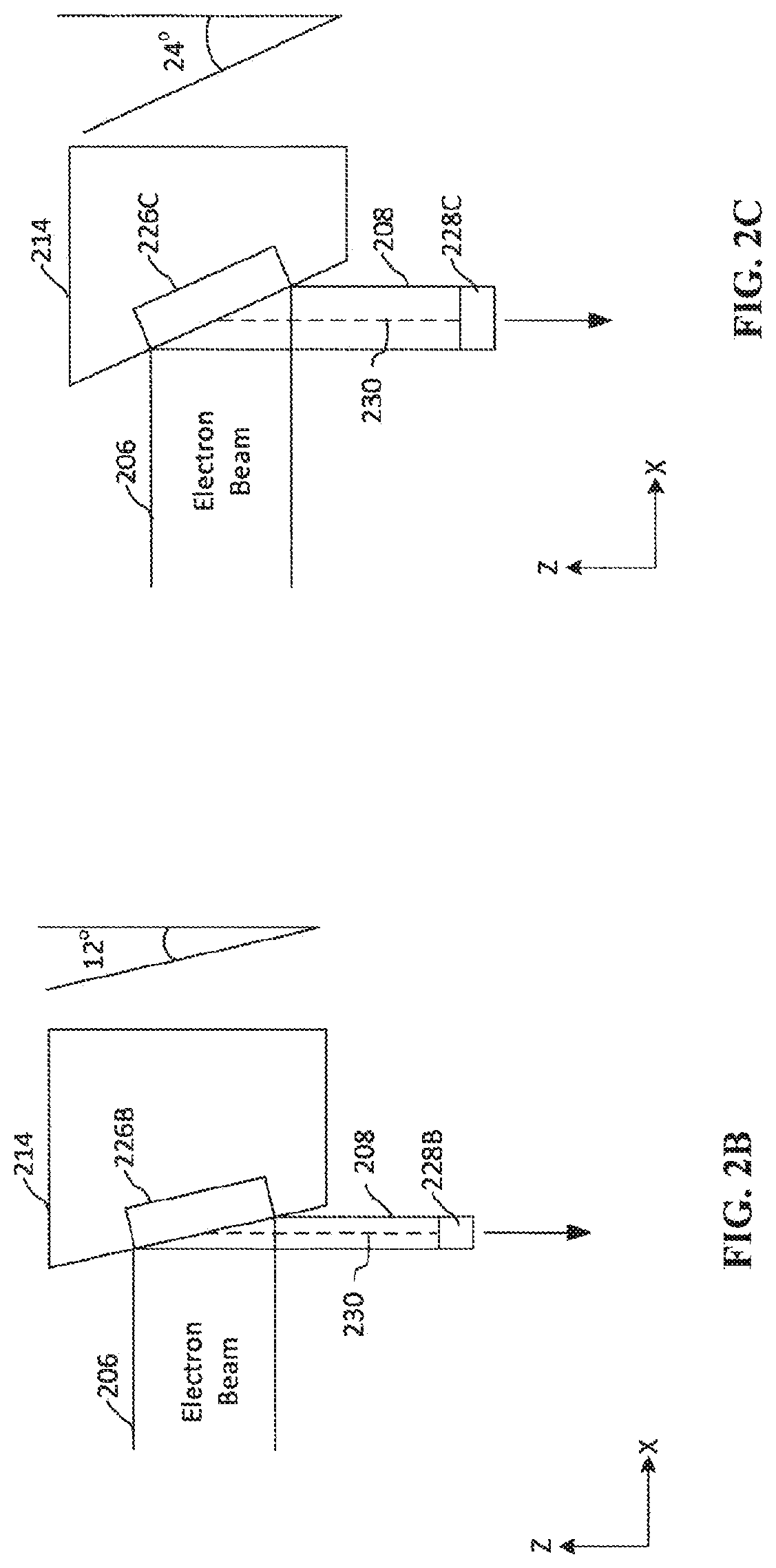
[0040] FIGS. 2B-2C depict two example of anodes having different angles. As shown in FIG. 2B, the electron beam 206 strikes the anode 214 in an area defining the anode focal spot 226B. The x-ray emission 208 from the anode focal spot 226B is emitted towards the target and has a cross-sectional area referred to as the effective focal spot 228B. The size of effective focal spot 226B affects the resolution of the final image produced by the tomosynthesis system 100, with smaller effective focal spots 226B generally allowing for higher resolution images. For instance, mammography systems may be designed to provide a 0.3 mm.times.0.3 mm effective focal spot for imaging, or a 0.1 mm.times.0.1 mm effective focal spot for high magnification images.
[0041] The size of the effective focal spot 228B is dependent on several factors, including the size of the anode focal spot 226B, and the angle of the face of the anode 214. By adjusting the angle of the face of the anode 214, one dimension (the x-dimension as depicted in FIGS. 2B-2C) of the effective focal spot 228B can be adjusted. As can be seen by comparing FIG. 2B with FIG. 2C, a smaller face angle for the anode results in a smaller effective focal spot 228B. For example, the face angle of the anode 214 in FIG. 2B is 12 degrees, whereas the face angle of the anode 214 in FIG. 2C is 24 degrees. As can be seen, the effective focal spot 228B is smaller than the effective focal spot 228C, despite being produced from the same anode focal spot (i.e., the same size electron beam). The x-ray emission 208 also has central line 230 indicating the central axis of the x-ray emission 208 directed towards the breast.
[0042] The size of the electron beam 206 is primarily based on the size of the active area of the cathode 212. The present technology utilizes a cathode 212 having an addressable array of electron-emitting sections to allow for controlled activation of discrete subsets of electron-emitting sections.
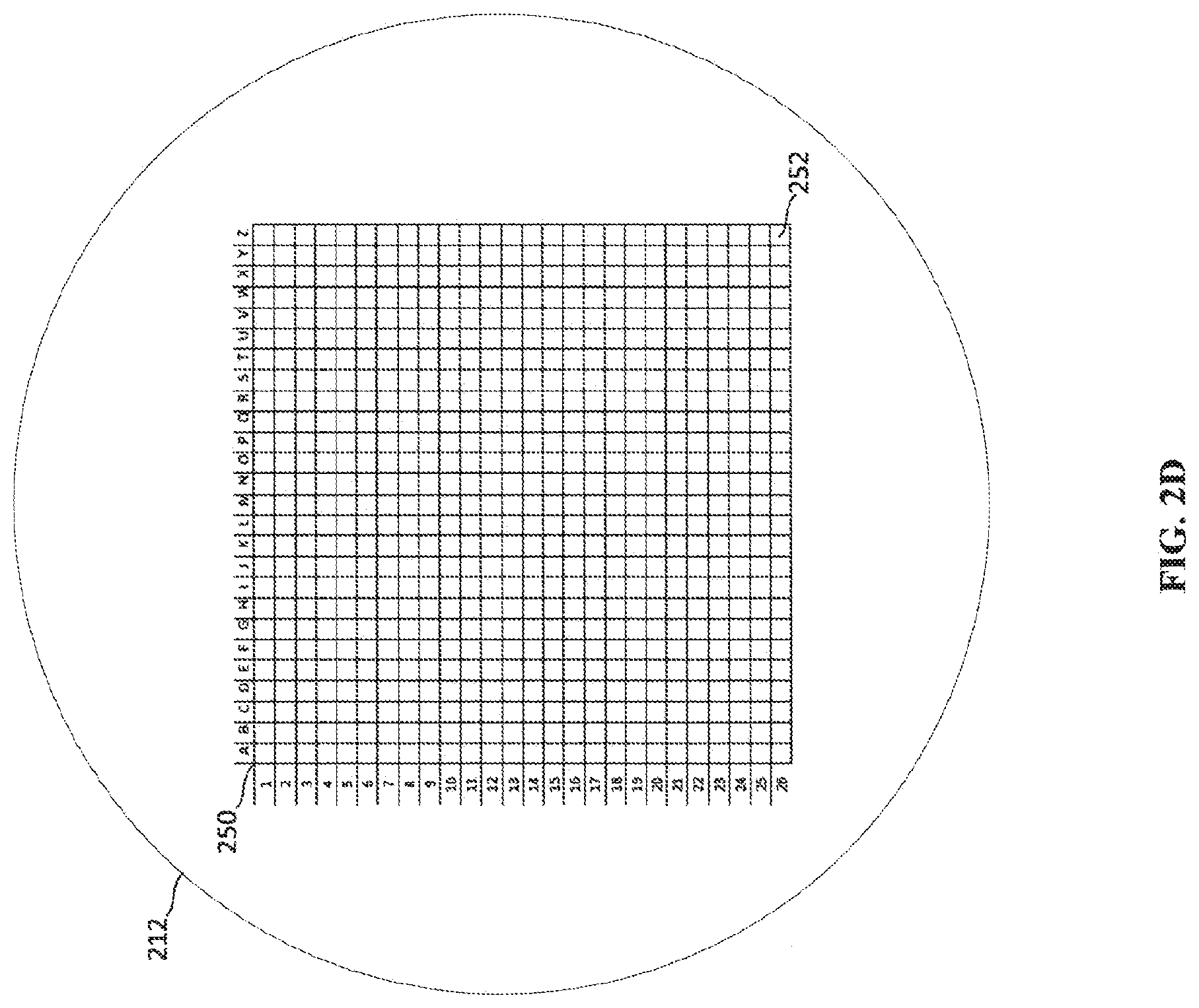
[0043] FIG. 2D depicts an example of a cathode 212 having an addressable array 250 of electron-emitting sections 252. In the example cathode 212 depicted in FIG. 2D, each electron-emitting section 252 of the addressable array 250 may include a single electron emitter or many electron emitters. In some examples, each electron-emitting section 252 may be individually addressable so that each electron-emitting section 252 may be activated individually. Such an example provides a high amount of flexibility in creating a pattern and size of an electron emission area defined by the activated electron-emitting sections 252. In another example, each row (e.g., rows 1-26) may be individually addressable. In such an example, the electron emission sections 252 are activated in a row-by-row manner. For instance, columns J through P may be activated to create a rectangular electron emission area. The example addressable array 250 in FIG. 2D is arranged based on standard Cartesian coordinates, however, other arrangements of electron emission sections are also contemplated.
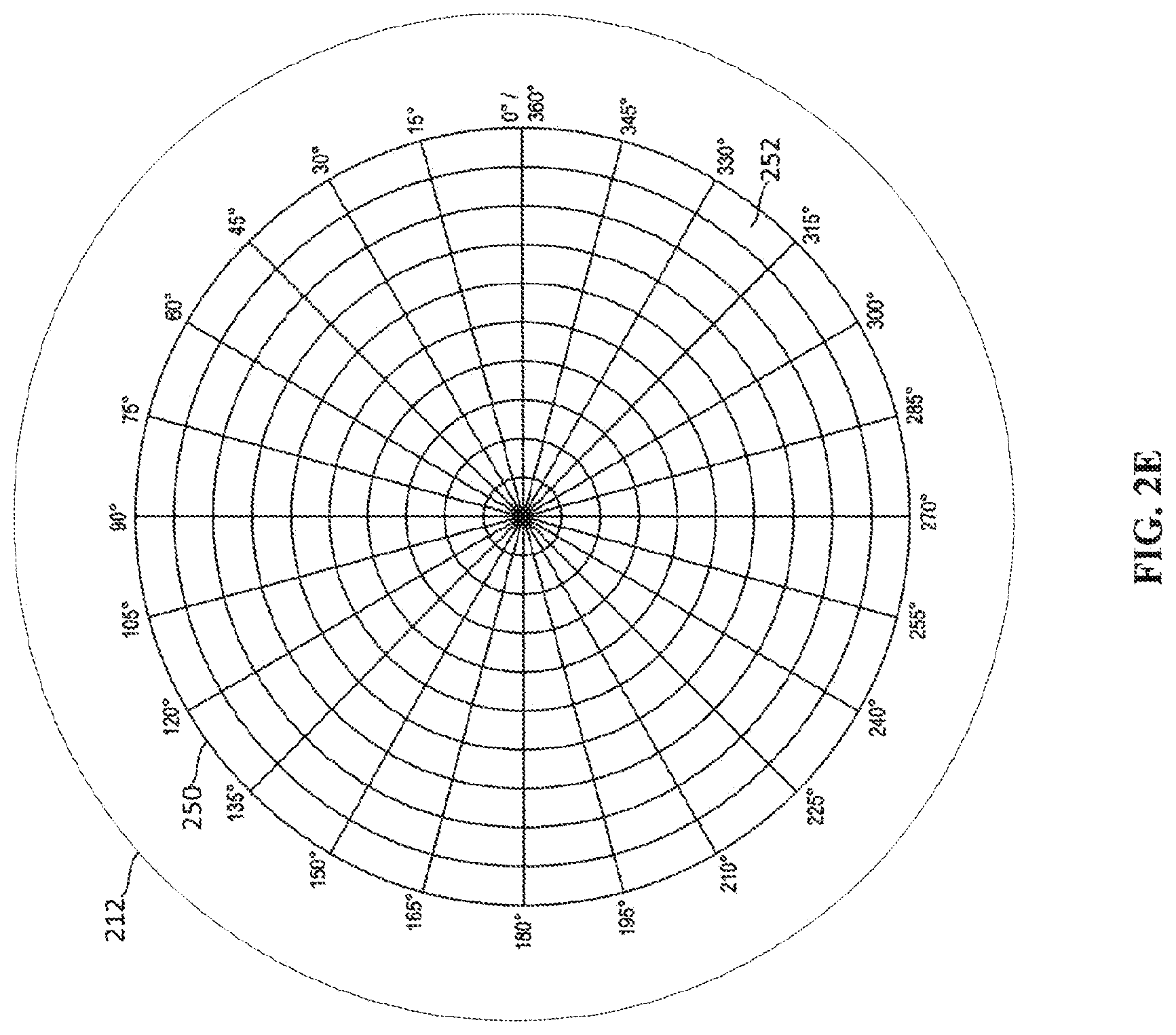
[0044] FIG. 2E depicts another example of a cathode 212 having an addressable array 250 of electron-emitting sections 252. The cathode 212 depicted in FIG. 2E is similar to the cathode 212 depicted in FIG. 2D, except that the addressable array 250 is arranged based on polar coordinates rather than Cartesian coordinates. In the example cathode 212 depicted in FIG. 2E, the each electron-emitting section 252 of the addressable array 250 may include a single electron emitter or many electron emitters. In some examples, each electron-emitting section 252 may be individually addressable so that each electron-emitting section 252 may be activated individually such an example provides a high amount of flexibility in creating a pattern and size of an electron emission area defined by the activated electron-emitting sections 252. In another example, each angular section of the addressable array 250 may be individually addressable. For instance, all the electron-emitting sections 252 between angles .theta. degrees to 15 degrees may be addressed similar to a row in the addressable array 250 depicted in FIG. 2D. In such an example, the electron emission sections 252 are activated angular section by angular section. Other arrangements based on different coordinate systems are also possible.
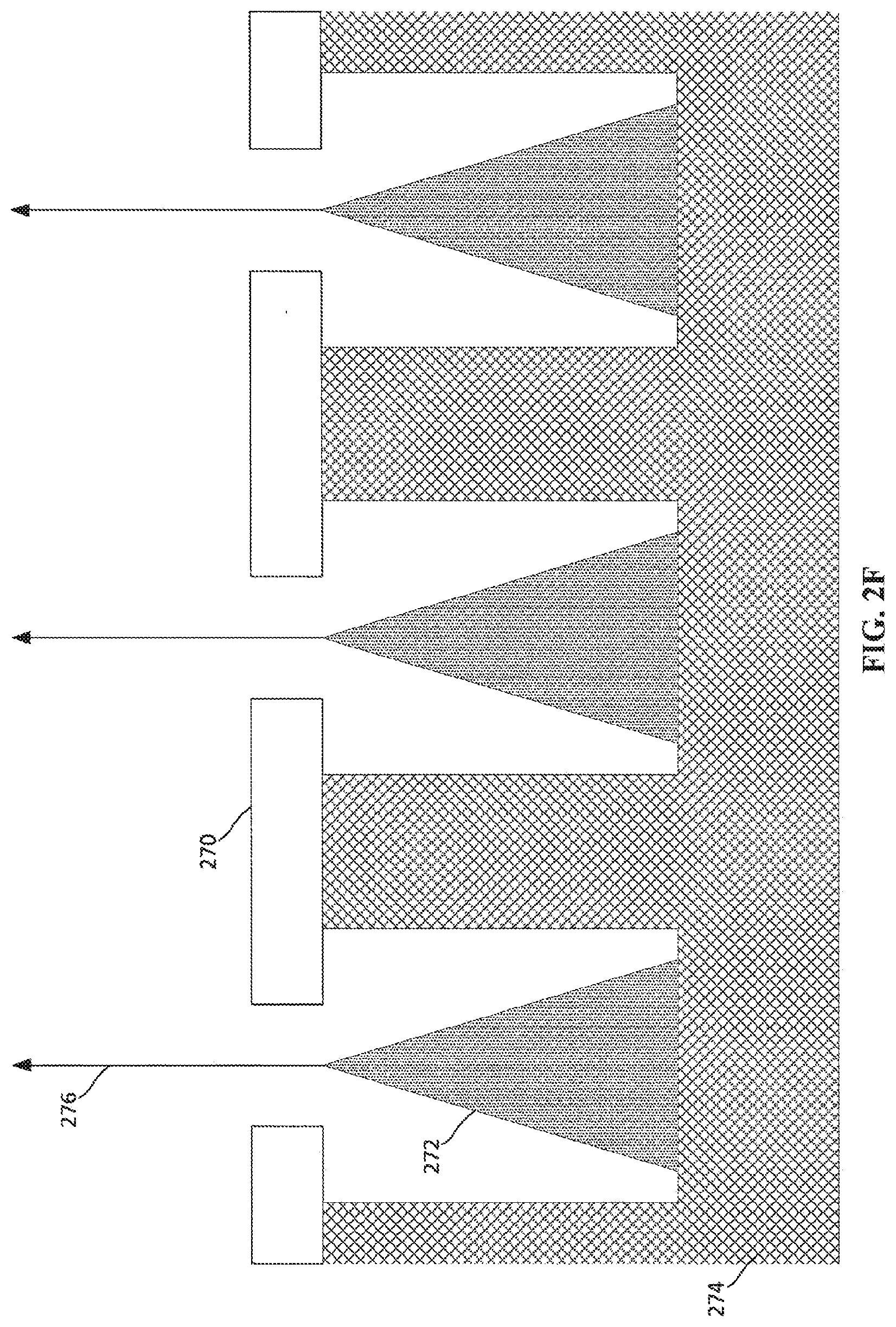
[0045] FIG. 2F depicts an example of electron emitters on a cathode 212. More specifically, FIG. 2F depicts an example of field-emission electron emitters. Field electronic emission is electron emission induced by an electrostatic field. This technology has been utilized in transistors, televisions, scanning electron microscopes, and other applications. The principles of field electron emission are generally known to a person of skill in the art. In the example depicted, each field-emission electron emitter includes a microtip 272 on a base 274. Above the microtip 272 is a gate layer 270. As a voltage difference is created between the gate layer 270 and the microtip 272, electrons 276 are emitted from the microtips 272. The field-emission electron emitters are affixed on the cathode 212 such that the electrons 276 project from the cathode 212 towards the anode 214 and are further accelerated based on the high-voltage difference between the cathode 212 and the anode 214. In embodiments, each of the microtips 272 can be individually addressed and activated. In some embodiments, rows or sections of the microtips 272 can be addressed and activated. In an example, the base 274 may be made of a silicon material, the microtips 272 may be made from a molybdenum or tungsten material, and the gate layer 270 may be made from a chromium, hafnium, niobium, or other conductive material. In other embodiments, the field-emission electron emitter may be a carbon-nanotube field emitter.
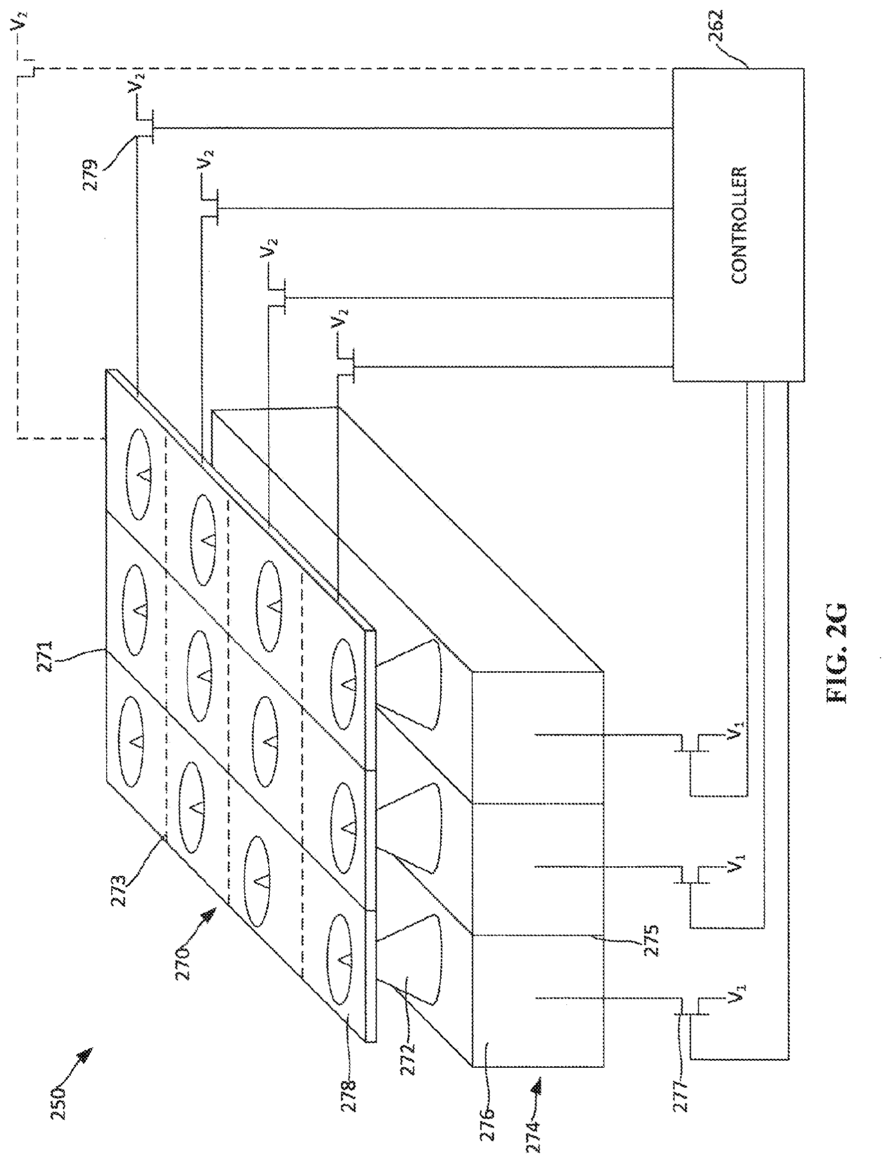
[0046] FIG. 2G depicts a portion of an addressable array 250 of field-emission electron emitters on a cathode (not shown). The addressable array 250 includes multiple field-emission emitters, which each include a microtip 272. Each microtip 272 is attached to a base 274. Spaced apart from the microtips 272 is a gate layer 272. The gate layer 272 defines a hole associated with each of the microtips 272 to allow for the emission of electrons when a selected electron emitter is activated. The base 274 may be divided into different sections by a base separator 275 that substantially prevents current from flowing from one side of the base separator 275 to the other side of the base separator 275. By including base separators 275, the voltage for the sectioned portions 276 of the base 274 can be individually controlled. In examples, controlling the voltage for each base section 276 also allows for control of the voltage on the corresponding microtip(s) 272 attached to the base section 276. For example, the base 274 may include base separators 275 to create rows of microtips 272. In such an example, a voltage may be applied to each row of microtips 272. In other examples, base separators 275 may be incorporated into the base 274 to separate each individual microtip 272. In such an example, a voltage may be applied to each discrete microtip 272.
[0047] The voltage to each base section 276 may be controlled through a set of base transistors 277. A base transistor 277 is connected to each base section 276 for which individual control and addressability is desired. In a configuration, the gates or bases of the base transistors 277 are connected to a controller 262 so that the controller 262 is able control each of the base transistors 277. Depending on the application, another end of the base transistor 277, such as the drain or collector, is connected to the base section 276 for which control is desired. The third end of the base transistor 277, such as the source or emitter, is connected to voltage source V1. In some examples, the voltage V1 is 0V or a ground with respect to a corresponding section of the gate layer 270.
[0048] The gate layer 270 may be sectioned similarly to the base 274 to allow for control of electron emission from each of the microtips 272 or a row of microtips 272. The gate layer 270 may include gate layer row separators 271 to separate the gate layer sections 278 above of a row of microtips 272. The gate layer 270 may also include gate layer column separators 273 to separate gate layer sections 278 above columns of microtips 272. The gate layer separators 271, 273 substantially prevent current from flowing from one side of the gate layer separator 271, 273 to the other side or the gate layer separator 271, 273. The gate layer separators 271, 273 may be arranged so that individual rows or columns of microtips 272 can be controlled and activated. The gate layer separators 271, 273 may also be arranged so that individual microtips 272 can be controlled and activated. The gate layer separators 271, 273 may also be arranged to encompass shared section of microtips 272.
[0049] The voltage to each gate layer section 278 may be controlled through a set of gate layer transistors 279. A gate layer transistor 279 is connected to each gate layer section 278 for which individual control and addressability is desired. For instance, there may be one gate layer transistor for each row of electron-emitting sections, each electron-emitting section, or each subset of electron-emitting sections, depending on the application and configuration. In a configuration, the gates or bases of the gate layer transistors 279 are connected to the controller 262 so that the controller is able to control each of the gate layer transistors 279. Depending on the application, another end of each gate layer transistor 279, such as the drain or collector, is connected to the gate layer section 278 for which control is desired. The third end of the base transistor, such as the source or emitter, is connected to voltage source V2. In some examples, the voltage V2 is approximately 100V greater than the corresponding base section voltage V1.
[0050] As discussed above, activation of a microtip 272 occurs when a voltage difference between the microtip 272 and the gate layer 270 is sufficiently large. By utilizing the various separators and transistors in the manner described relative to FIG. 2G, microtips 272 can be activated individually, by row, or by any other shaped section be controlling the voltage difference between a base section 276 and a corresponding gate layer section 278 directly above the respective base section 276. In some embodiments, only one of the base transistors 277 or the gate layer transistors 279 may be utilized. For example, the entire base may be grounded and the individual gate layer sections 278 are controlled via the gate layer transistors 279. In such an example, a voltage of 100V above ground may be selectively applied to each of the gate layer sections 278 by controlling the gate layer transistors 279. In another example, the entire gate layer 270 may be held at a voltage V2 and the respective voltages V1 of sections 276 of the base 274 may be individually controlled through the base transistors 277.
[0051] The gate layer 270, microtips 272, base 274, base transistors 277, and the gate layer transistors 279 may all be manufactured into a single integrated circuit or microchip that is incorporated into the cathode 212. The controller 262 may then control the microchip or integrated circuit through an interface designed to allow for a voltage to be discretely applied to each separated section 278 of the gate layer 270 and/or each separated section 276 of the base 274. Other potential control and manufacturing schemes are also contemplated and may be implemented.
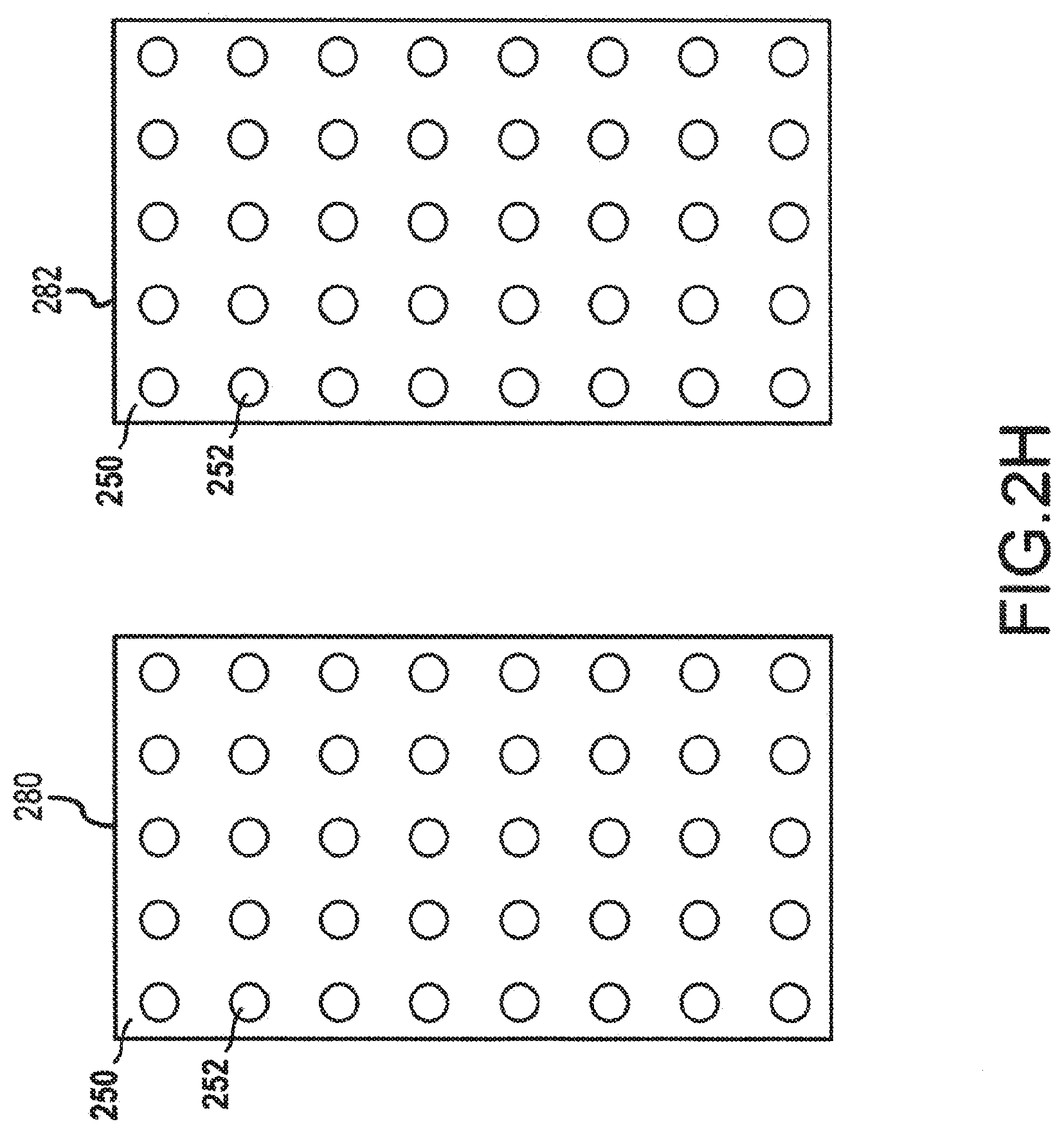
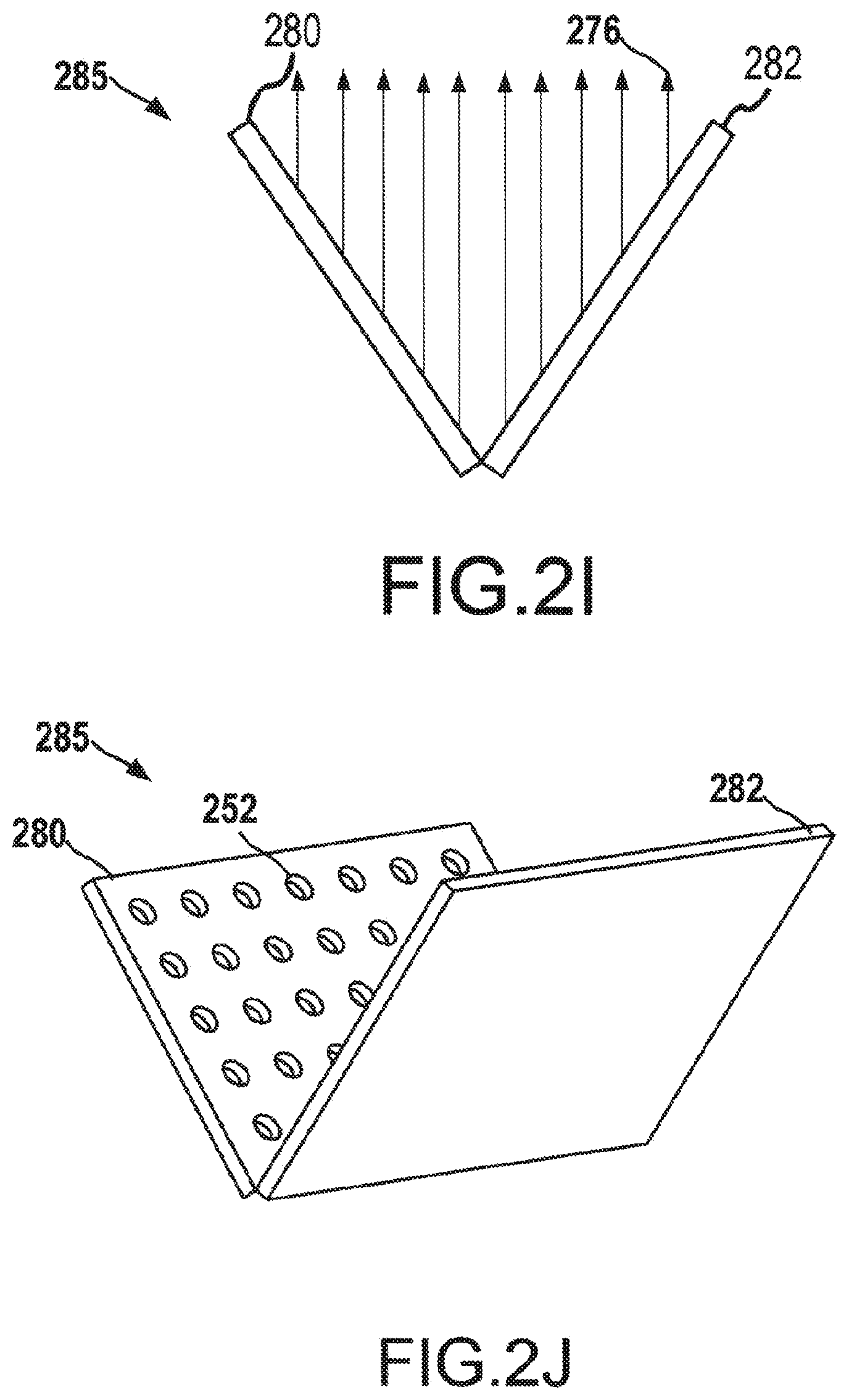
[0052] Three-dimensional (3D) addressable arrays may also be manufactured to increase the electron density emitting from a cathode having the 3D addressable array. For example, the addressable arrays may be arranged to form a parabolic or cone shape to emit additional electrons than what would be possible with a single flat surface. As compared to two-dimensional addressable array, a 3D addressable array has a distribution of electron-emitting sections across the x-direction, the y-direction, and the z-direction when incorporated into a cathode of an x-ray tube, such as the x-ray tube depicted in FIG. 2A. Such a 3D addressable array may be manufactured as a single component or generated from multiple planar surfaces, among other potential manufacturing methods. FIG. 2H depicts two cathode plates 280, 282 having addressable arrays 250 of electron-emitting sections 252. The electron-emitting sections 252 may be field emission electron emitting sections and may be individually addressable, as discussed above with reference to FIGS. 2F-2G. The cathode plates 280, 282 may be combined to form a v-shaped 3D addressable array for use in a cathode, as shown in FIGS. 2I and 2J. FIG. 2I depicts a side view of the v-shaped 3D addressable array 285. Each of the electron-emitting sections 252 of the cathode plates 280, 282 may emit electrons 276. As can be seen from FIG. 2I, by arranging the cathode plates in a v-shape, the maximum electron density that can be emitted from the v-shaped addressable array 285 is greater than the maximum electron density than may be emitted from a single planar addressable array. While only two cathode plates 280, 282 have been depicted herein to create the 3D addressable array 285, additional smaller cathode plates may also be used to further approximate a parabolic or u-shape or v-shape for the 3D addressable array 285. For example, each row of electron-emitting sections 252 may be manufactured on a discrete cathode plate, and each cathode plate may be connected at an appropriate angle to each other cathode plate to approximate a parabolic shape.
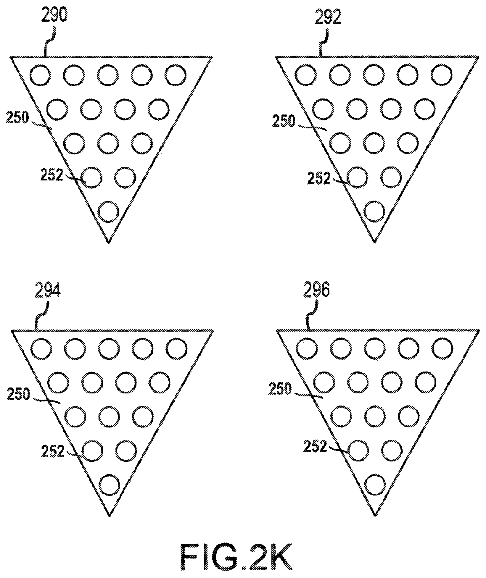
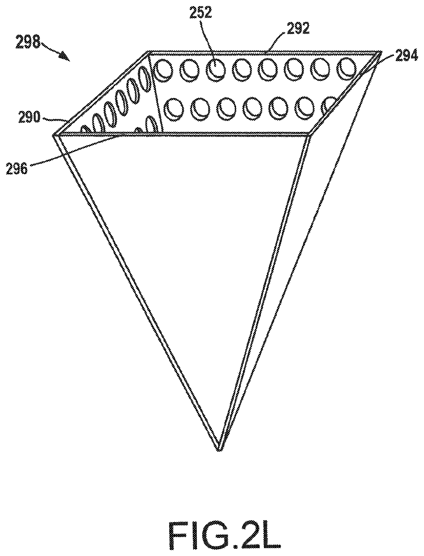
[0053] Multiple cathode plates may also be utilized to approximate a cone shape or a hollow pyramid shape for a 3D addressable array. FIG. 2K depicts a set of cathode plates 290, 292, 294, 296 having addressable arrays 250 of electron-emitting sections 252. Similar to the electron-emitting sections 252 of cathode plates 280, 282 depicted in FIGS. 2H-J, the electron-emitting sections 252 in cathode plates 290, 292, 294, 296 may be field emission electron emitting sections and may be individually addressable, as discussed above with reference to FIGS. 2F-2G. The set of cathode plates 290, 292, 294, 296 may be used to manufacture a pyramidal 3D addressable array 398, shown in FIG. 2L. FIG. 2L depicts a perspective view of the pyramidal 3D addressable array 398 manufactured from the set of cathode plates 290, 292, 294, 296. By using a pyramidal 3D addressable array 298 in a cathode, a higher electron density may be generated than can be generated from a single planar surface of electron-emitting sections 252 or a v-shaped 3D addressable array. While only four cathode plates 290, 292, 294, 296 have been depicted herein to create the 3D addressable array 298, additional smaller cathode plates may also be used to further approximate a conical shape for the 3D addressable array 298. For example, each row of electron-emitting sections 252 may be manufactured on a discrete cathode plate, and each cathode plate may be connected at an appropriate angle to each other cathode plate to approximate a parabolic shape. Further, while the term cathode plate has been used herein to describe the planar surfaces used in manufacturing the 3D addressable arrays, one having skill in the art will appreciate that the concept of a cathode plate is not limited solely to a plate structure. Any surfaces or structures including an addressable array of electron emitting sections may be used as, and considered to be a cathode plate or its equivalent.
[0054] Operation of a 3D addressable array, such as the v-shaped 3D addressable array 285 or the pyramidal 3D addressable array, may be similar to the control of the addressable array 250 as discussed above with reference to FIG. 2G. For instance, somewhat linear control of the electron-emitting sections 252 may still be accomplished, however, three-dimensional control of the electron-emitting sections 252 may also be accomplished. By controlling the electron-emitting sections 252 in three dimensions, the size and shape of the focal spot may be further modified. In an example of a cone-shaped 3D addressable array or a pyramidal 3D addressable array 298, two of the cathode plates, such as cathode plates 290, 294 may be used to move the focal spot linearly, while the other two cathode plates 292, 296 may be used to control or direct the electrons being emitted by the cathode plates 290, 294. For instance, electrons emitted from one cathode plate will interact with electrons emitted from other cathode plates. By controlling the addressable arrays, such interactions may be further manipulated or utilized in generating a desired focal spot. As such, a first set of electron-emitting sections may be used for shifting the focal spot, and a second set of electron-emitting sections may be used to modify the electrons emitted from those electron-emitting sections.
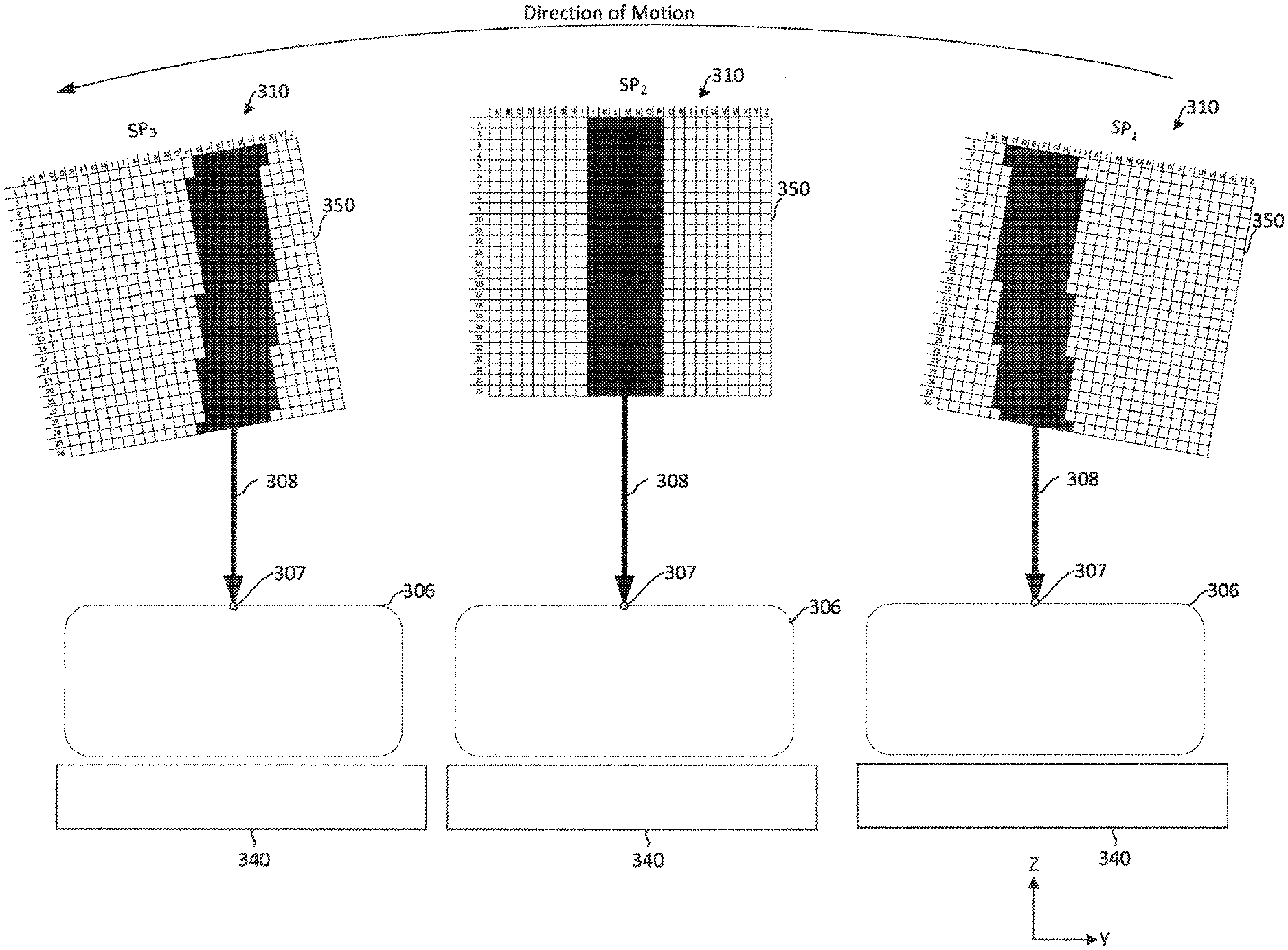
[0055] FIG. 3A depicts movement of an x-ray source 310 in the breast tomosynthesis system 300. The movement of the x-ray source 310 is substantially the same as the movement of the x-ray source 310 discussed above with reference to FIG. 1B. The x-ray source 310 rotates relative to the breast 306 and the x-ray source 310 emits an x-ray emission 308 at multiple positions P1-P7 during the rotation. For example, when the x-ray source reaches a position, such as position P4, the x-ray source will begin emitting an x-ray emission 308 towards the breast 306. The x-ray emission 308 passes through the breast before reaching the detector 340. The emission of x-rays from the x-ray source 310 for a period of approximately 10 ms to 100 ms. During that period of emission, the x-ray source 310 continues to move relative to the breast 306 and the detector 340, as shown by the dashed circles and box surrounding the x-ray source 310 at P4. In traditional systems, from the perspective of the breast 306, an effective focal spot appears to move or grow in size during emission while the x-ray source 310 is moving. In the present technology, different subsets of electron-emitting sections on the cathode can be activated during the movement of the x-ray source 310 to compensate for the movement of the x-ray source 310 in order to make the effective focal spot appear stationary from the perspective of the breast. For example, if the x-ray source 310 is moving in a counter-clockwise direction, subsets of electron-emitting sections are consecutively activated in the clockwise direction. FIGS. 3B and 3C depict two examples of activating subsets of electron-emitting sections to compensate for movement of the x-ray source 310 around position P4.
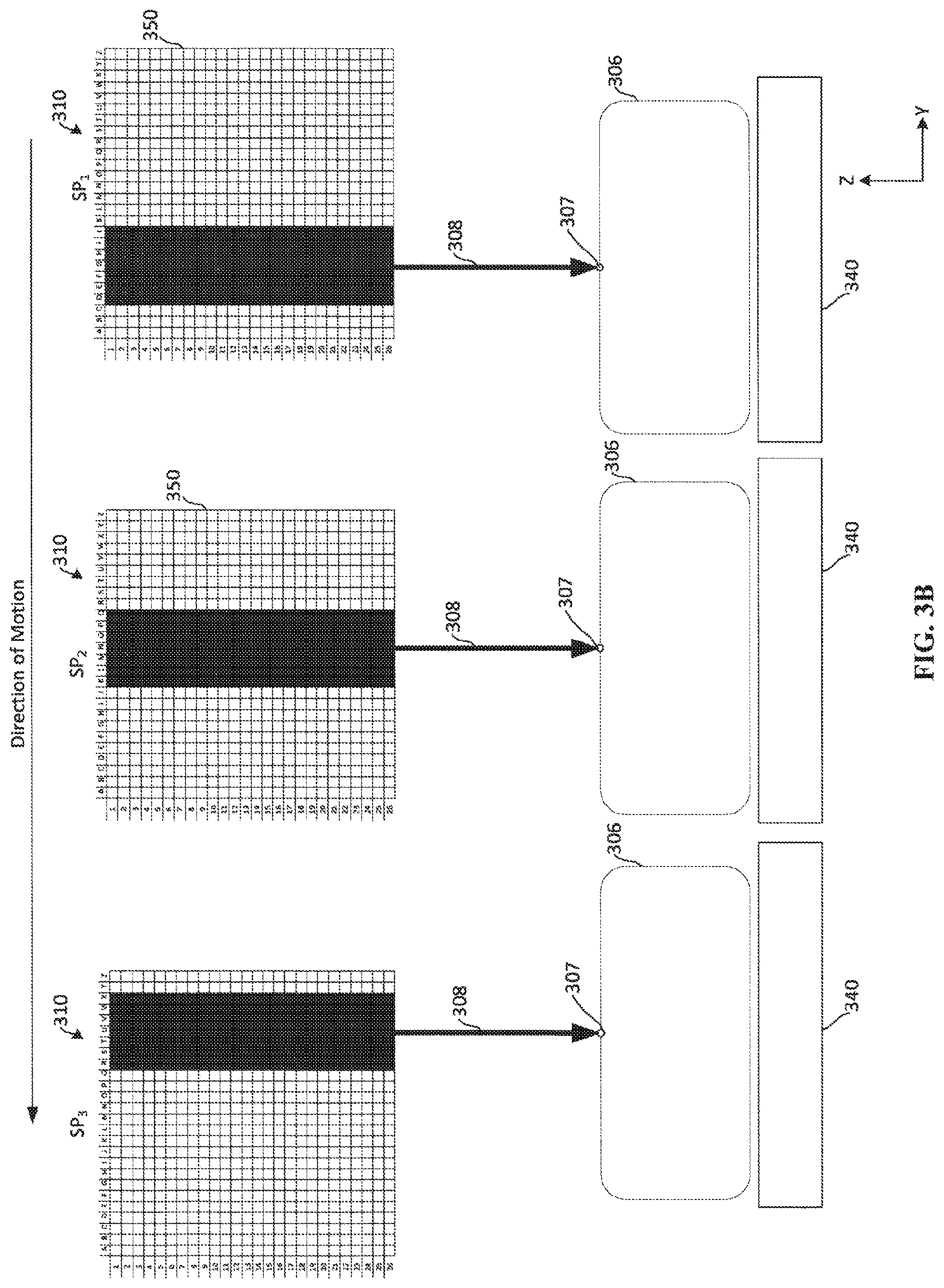
[0056] FIG. 3B depicts an example of activating electron-emitting sections during movement of the x-ray source 310. The addressable array 350 on the cathode of an x-ray source 350 is depicted in FIGS. 3B-3C. As will be appreciated, upon activation of electron-emitting sections in the addressable array 350, electrons emitting from the active sections accelerate to an anode (not shown) and x-rays are generated from the anode, thus causing an x-ray emission 308 to be directed towards the breast 306, as discussed above with reference to FIGS. 2A-2G. As x-ray source 310 moves through a position, such as position P4 in FIG. 3A, the x-ray source 310 emits an x-ray emission 308. While emitting x-rays, the x-ray source 310 passes through multiple sub-positions SP1-SP3. FIG. 3B depicts the x-ray source 310 moving in a counter-clockwise direction through sub-positions SP1-SP3. In the example depicted in FIG. 3B, the movement through the sub-positions SP1-SP3 is approximated to be linear motion, although the actual motion of the x-ray source may be rotational around the x-axis (e.g., as defined by the breast). When the x-ray source 310 is in sub-position SP1, a first subset of electron-emitting sections of the addressable array 350 is activated. The subset of electron-emitting sections at each sub-position is depicted by shading in the addressable array 350. For instance, at sub-position SP1, rows D-J are included in a first subset of electron-emitting sections. At sub-position SP1, activation of the first subset of electron-emitting sections causes an x-ray emission 308 to be emitted from the x-ray-source 310 towards a single location 307 on the breast 306. For example, the center line of the x-ray emission 308 is directed at a single location 307 on the breast 306.
[0057] As the x-ray source 310 moves from sub-position SP1 to SP2, a second subset of electron-emitting sections of the addressable array 350 is activated. As shown in FIG. 3B, the second subset of electron-emitting sections includes rows K-Q of the addressable array 350. By shifting the active electron-emitting sections from the first subset to the second subset of electron-emitting sections, the x-ray emission 308 from the x-ray source 310 continues to be directed at the same single location 307 on the breast 306. More specifically, the center line of the x-ray emission 308 continues to be directed to the single location 307 on the breast 306. Also, from the perspective of the breast 306 and the detector 340, the effective focal spot of the x-ray emission remains substantially the same shape, size, and location as the x-ray source moves from sub-position SP1 to SP2.
[0058] As the x-ray source 310 moves from sub-position SP2 to SP3, a third subset of electron-emitting sections of the addressable array 350 is activated. As shown in FIG. 3B, the third subset of electron-emitting sections includes rows R-X of the addressable array 350. By shifting the active electron-emitting sections from the second subset to the third subset of electron-emitting sections, the x-ray emission 308 from the x-ray source 310 continues to be directed at the same single location 307 on the breast 306. More specifically, the center line of the x-ray emission 308 continues to be directed to the single location 307 on the breast 306. Also, from the perspective of the breast 306 and the detector 340, the effective focal spot of the x-ray emission remains substantially the same shape, size, and location as the x-ray source moves from sub-position SP1 to SP2 and from SP2 to SP3.
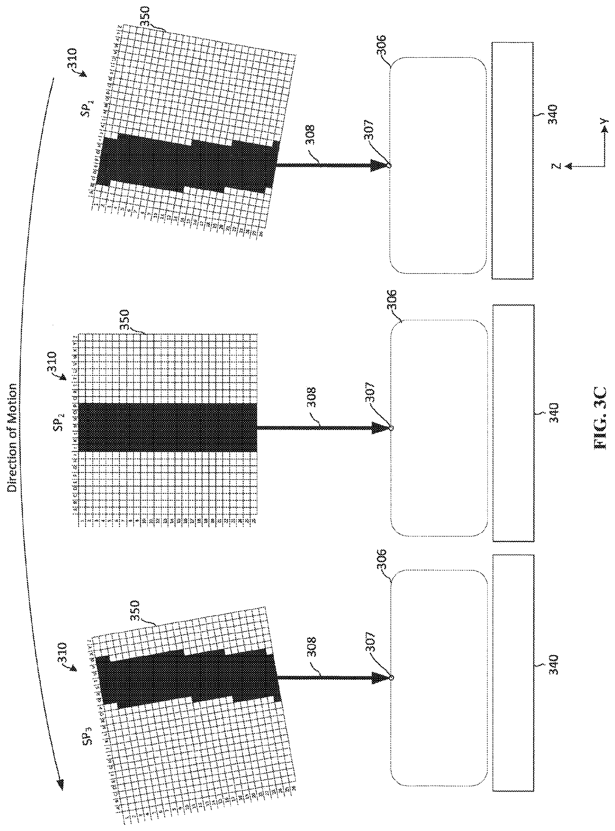
[0059] By utilizing a linear approximation of the rotational motion of the x-ray source 310, activation of whole rows of the addressable array 250 is performed, as shown in FIG. 3B. In applications requiring further precision, however, the linear approximation may not be sufficient. FIG. 3C depicts an example of activating electron-emitting sections during movement of the x-ray source 310 that accounts for rotational aspects of the x-ray source 310. As x-ray source 310 moves through a position, such as position P4, the x-ray source 310 emits an x-ray emission 308. FIG. 3C depicts the x-ray source 310 moving in a counter-clockwise direction through sub-positions SP-SP3. When the x-ray source 310 is in sub-position SP1, a first subset of electron-emitting sections of the addressable array 350 is activated. For instance, at sub-position SP1, portions of electron-emitting sections from rows C-M of the addressable array 350 are a activated. In contrast to the example depicted in FIG. 3B, some of the rows are not fully activated so as to account for the rotational movement of the x-ray source 310. At sub-position SP1, activation of the first subset of electron-emitting sections causes an x-ray emission 308 to be emitted from the x-ray-source towards a single location 307 on the breast 306. For example, the center line of the x-ray emission 308 is directed at a single location 307 on the breast 306.
[0060] As the x-ray source 310 moves from sub-position SP1 to SP2, a second subset of electron-emitting sections of the addressable array 350 is activated. As shown in FIG. 3B, the second subset of electron-emitting sections includes electron-emitting sections rows J-P of the addressable array 350. By shifting the active electron-emitting sections from the first subset to the second subset of electron-emitting sections, the x-ray emission 308 from the x-ray source 310 continues to be directed at the same single location 307 on the breast 306. More specifically, the center line of the x-ray emission 308 continues to be directed to the single location 307 on the breast 306. Also, from the perspective of the breast 306 and the detector 340, the effective focal spot of the x-ray emission remains substantially the same shape, size, and location as the x-ray source 310 moves from sub-position SP1 to SP2.
[0061] As the x-ray source 310 moves from sub-position SP2 to SP3, a third subset of electron-emitting sections of the addressable array 350 is activated. As shown in FIG. 3B, the third subset of electron-emitting sections includes electron-emitting sections from rows M-W of the addressable array 350. In the example depicted in FIG. 3C, the third subset includes electron-emitting sections from the second subset, and the first subset includes electron-emitting sections from the first subset. In other examples, the subsets of electron-emitting sections may not overlap. By shifting the active electron-emitting sections from the second subset to the third subset of electron-emitting sections, the x-ray emission 308 from the x-ray source 310 continues to be directed at the same single location 307 on the breast 306. More specifically, the center line of the x-ray emission 308 continues to be directed to the single location 307 on the breast 306. Also, from the perspective of the breast 306 and the detector 340, the effective focal spot of the x-ray emission remains substantially the same shape, size, and location as the x-ray source 310 moves from sub-position SP1 to SP2 and from SP2 to SP3. Other subsets of electron-emitting sections may also be utilized to cause the center line of the x-ray emission 308 to remain substantially directed towards the single location 307. For example, while the subsets of the electron-emitting sections shown in FIGS. 3B-3C are shown as substantially rectangular, the geometry of the shape of the subsets of electron-emitting sections may vary depending on the application. For instance, depending on the emission characteristics, the gap between the anode and cathode, anode angle, and other anode-cathode alignment geometries, the shape of the electron-emitting sections may be approximately a triangle, rectangle, other regular or irregular polygon, a circle, an oval, or any other curved or irregular curved shape. These shapes may need further fine optimization to control the desired focal spot shape (e.g., turning on or off individual active electron emitting elements). Additionally as the x-ray source 310 is moved as described herein, the shape of the active subset of electron-emitting sections may utilize dynamic real-time adaptation to control the effective focal spot and x-ray geometries.
[0062] FIG. 4 depicts a method 400 of using a tomosynthesis system for imaging. At operation 410, a radiation source, such as an x-ray source, is moved relative to a target, such as a breast. As the radiation source is moving relative to the target, a first subset of electron-emitting sections in an addressable array on a cathode of the radiation source is activated at operation 410. Activation of the first subset of electron-emitting sections causes an x-ray emission to be directed to a single location on the target, such as the breast. At operation 420, while the radiation source continues moving, a second subset of electron-emitting sections of the addressable array on the cathode is activated to compensate for movement of the radiation source from a first position to a second position. Activation of the second subset of electron-emitting sections causes the x-ray emission to continue to be directed to the single location on the target. In embodiments, activation of the second subset of electron-emitting sections causes the effective focal spot of the x-ray emission to appear stationary from the perspective of the target. From the perspective of the target, the effective focal spot may also appear to remain unchanging in size, shape, and position during the x-ray emission from the first and second subset of electron-emitting sections. As the radiation source moves through the first position and the second position, the radiation emitting from the radiation source is detected at operation 440. After the radiation source has emitted a sufficient amount of time for imaging, such as 10 ms to 100 ms, the electron-emitting sections are deactivated at operation 450. While only two subsets of electron-emitting sections are discussed with reference to method 400, many more subsets may be utilized to more precisely compensate for movement of the radiation source while emitting radiation. Also, when shifting subsets of electron-emitting sections, the shift may be to another subset of electron-emitting sections in either the z-direction, the y-direction, or both directions with respect to the coordinate system depicted in the figures. As will be appreciated, shifting from one subset of electron-emitting sections to another set of electron emitting sections of the cathode will cause a shift in the anode focal spot.
[0063] While primarily discussed herein as activating electron-emitting subsets to compensate for movement of an x-ray source, activating electron-emitting subsets may also be performed for other purposes. For instance, activating electron-emitting subsets may be performed on a stationary radiation source to make the x-ray emission appear to be moving from the perspective of the breast.
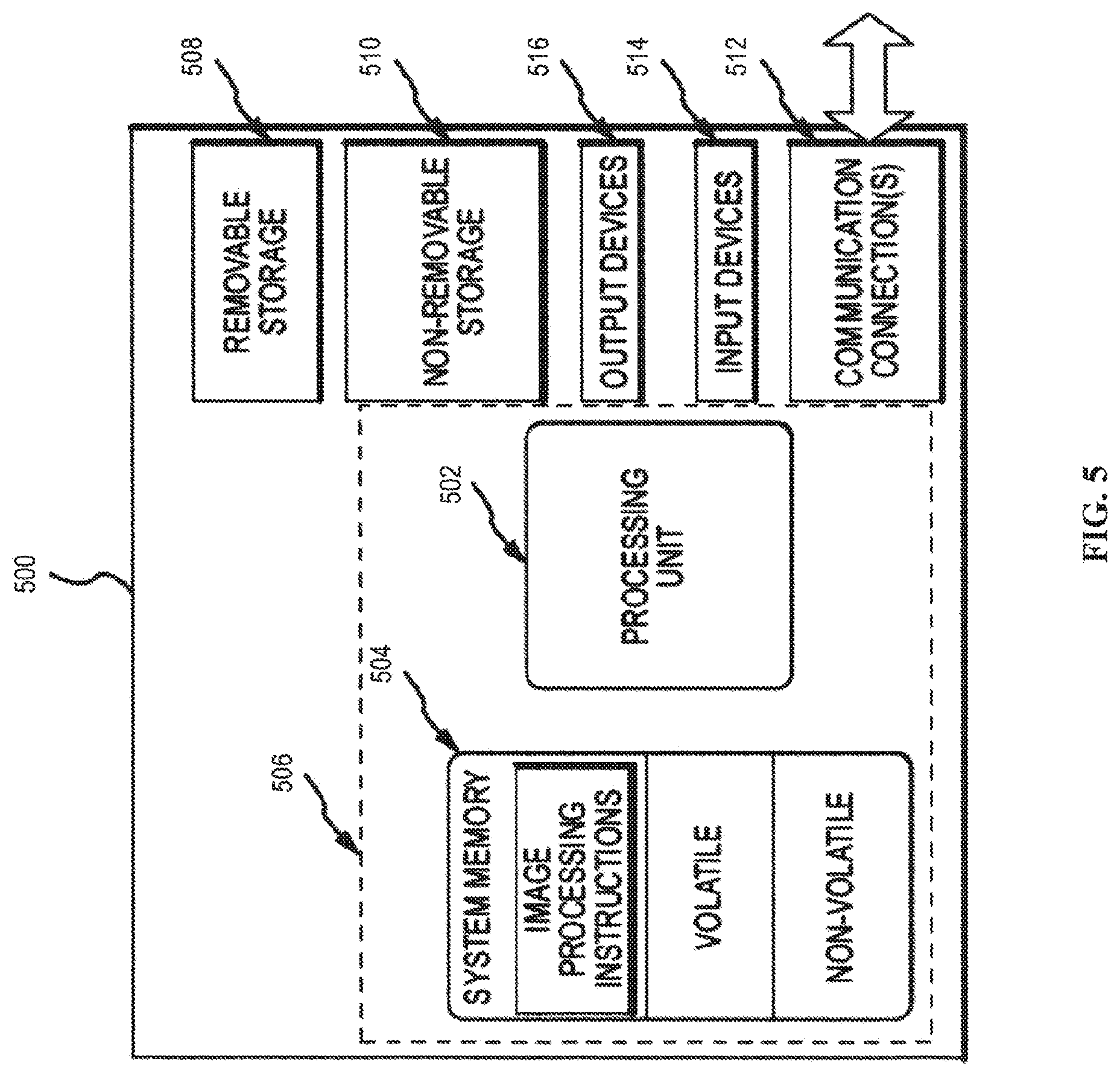
[0064] FIG. 5 illustrates one example of a suitable operating environment 500 in which one or more of the present embodiments can be implemented. This operating environment may be incorporated directly into a tomosynthesis system, or may be incorporated into a computer system discrete from, but used to control, a tomosynthesis system such as described herein, such as the controller. This is only one example of a suitable operating environment and is not intended to suggest any limitation as to the scope of use or functionality. Other well-known computing systems, environments, and/or configurations that can be suitable for use include, but are not limited to, imaging systems, personal computers, server computers, hand-held or laptop devices, multiprocessor systems, microprocessor-based systems, programmable consumer electronics such as smart phones, network PCs, minicomputers, mainframe computers, tablets, distributed computing environments that include any of the above systems or devices, and the like.
[0065] In its most basic configuration, operating environment 500 typically includes at least one processing unit 502 and memory 504. Depending on the exact configuration and type of computing device, memory 504 (storing, among other things, instructions to perform the image acquisition and processing methods disclosed herein) can be volatile (such as RAM), non-volatile (such as ROM, flash memory, etc.), or some combination of the two. This most basic configuration is illustrated in FIG. 5 by dashed line 506. Further, environment 500 can also include storage devices (removable, 508, and/or non-removable, 510) including, but not limited to, magnetic or optical disks or tape. Similarly, environment 500 can also have input device(s) 514 such as touch screens, keyboard, mouse, pen, voice input, etc., and/or output device(s) 516 such as a display, speakers, printer, etc. Also included in the environment can be one or more communication connections 512, such as LAN, WAN, point to point, Bluetooth, RF, etc.
[0066] Operating environment 500 typically includes at least some form of computer readable media. Computer readable media can be any available media that can be accessed by processing unit 502 or other devices comprising the operating environment. By way of example, and not limitation, computer readable media can comprise computer storage media and communication media. Computer storage media includes volatile and nonvolatile, removable and non-removable media implemented in any method or technology for storage of information such as computer readable instructions, data structures, program modules or other data. Computer storage media includes, RAM, ROM, EEPROM, flash memory or other memory technology, CD-ROM, digital versatile disks (DVD) or other optical storage, magnetic cassettes, magnetic tape, magnetic disk storage or other magnetic storage devices, solid state storage, or any other tangible medium which can be used to store the desired information. Communication media embodies computer readable instructions, data structures, program modules, or other data in a modulated data signal such as a carrier wave or other transport mechanism and includes any information delivery media. The term "modulated data signal" means a signal that has one or more of its characteristics set or changed in such a manner as to encode information in the signal. By way of example, and not limitation, communication media includes wired media such as a wired network or direct-wired connection, and wireless media such as acoustic, RF, infrared and other wireless media. Combinations of the any of the above should also be included within the scope of computer readable media.
[0067] The operating environment 500 can be a single computer operating in a networked environment using logical connections to one or more remote computers. The remote computer can be a personal computer, a server, a router, a network PC, a peer device or other common network node, and typically includes many or all of the elements described above as well as others not so mentioned. The logical connections can include any method supported by available communications media. Such networking environments are commonplace in offices, enterprise-wide computer networks, intranets and the Internet.
[0068] In some embodiments, the components described herein comprise such modules or instructions executable by computer system 500 that can be stored on computer storage medium and other tangible mediums and transmitted in communication media. Computer storage media includes volatile and non-volatile, removable and non-removable media implemented in any method or technology for storage of information such as computer readable instructions, data structures, program modules, or other data. Combinations of any of the above should also be included within the scope of readable media. In some embodiments, computer system 500 is part of a network that stores data in remote storage media for use by the computer system 500.
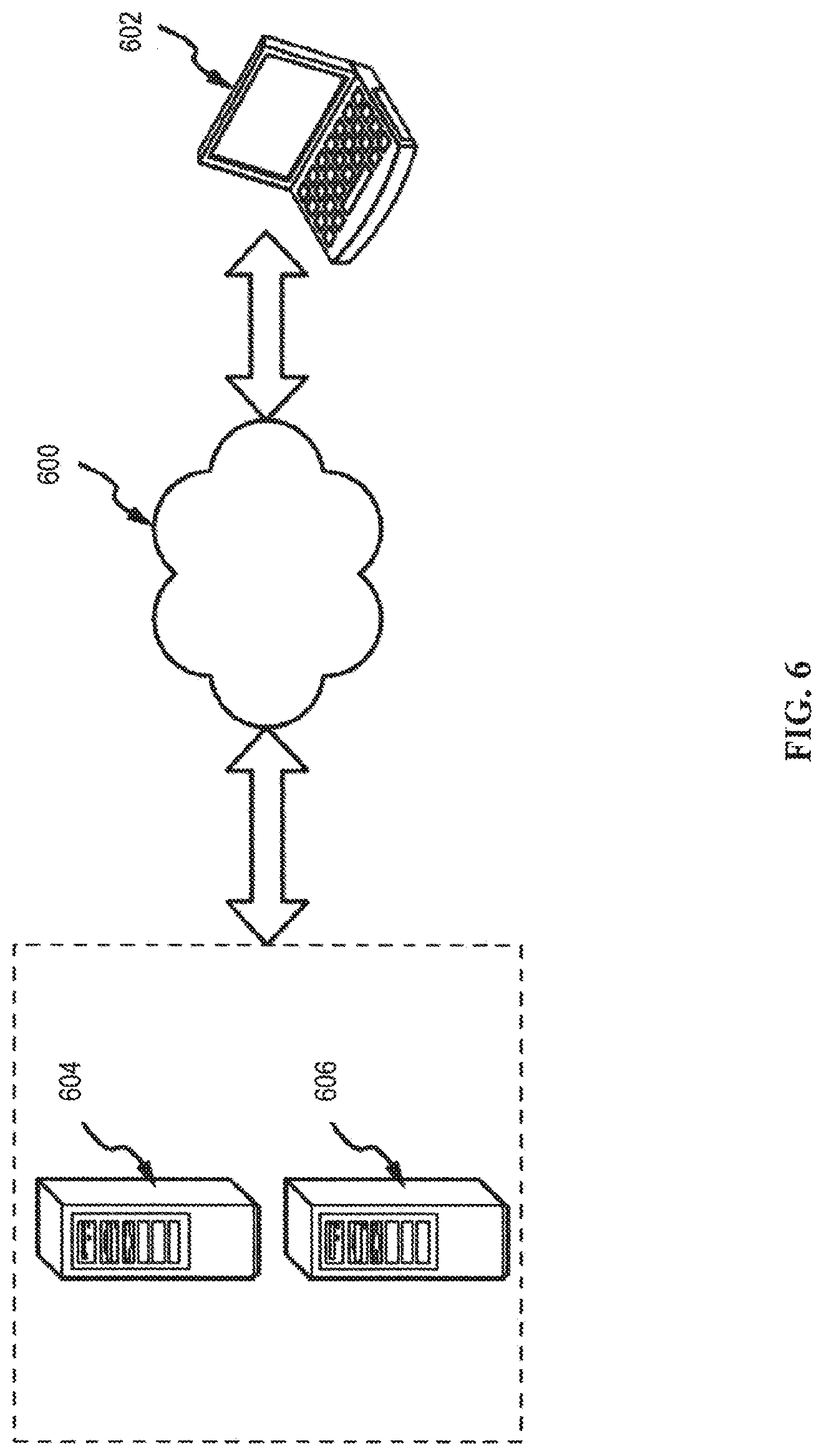
[0069] FIG. 6 is an embodiment of a network 600 in which the various systems and methods disclosed herein may operate. In embodiments, a client device, such as client device 602, may communicate with one or more servers, such as servers 604 and 606, via a network 608. In embodiments, a client device may be a laptop, a personal computer, a smart phone, a PDA, a netbook, or any other type of computing device, such as the computing device in FIG. 5. In embodiments, servers 604 and 606 may also be any type of computing device, such as the computing device illustrated in FIG. 5. Network 608 may be any type of network capable of facilitating communications between the client device and one or more servers 604 and 606. For example, the x-rays detected by the detector may be recognized locally in the tomosynthesis system and communicated to another computing device(s) for further processing, such as an image acquisition workstation. Examples of such networks include, but are not limited to, LANs, WANs, cellular networks, and/or the Internet.
[0070] In embodiments, the various systems and methods disclosed herein may be performed by one or more server devices. For example, in one embodiment, a single server, such as server 604 may be employed to perform the systems and methods disclosed herein, such as the method for utilizing the tomosynthesis system. Client device 602 may interact with server 604 via network 608. In further embodiments, the client device 602 may also perform functionality disclosed herein, such as scanning and image processing, which can then be provided to servers 604 and/or 606.
[0071] In alternate embodiments, the methods and systems disclosed herein may be performed using a distributed computing network, or a cloud network. In such embodiments, the methods and systems disclosed herein may be performed by two or more servers, such as servers 604 and 606. Although a particular network embodiment is disclosed herein, one of skill in the art will appreciate that the systems and methods disclosed herein may be performed using other types of networks and/or network configurations.
[0072] The embodiments described herein can be employed using software, hardware, or a combination of software and hardware to implement and perform the systems and methods disclosed herein. Although specific devices have been recited throughout the disclosure as performing specific functions, one of skill in the art will appreciate that these devices are provided for illustrative purposes, and other devices can be employed to perform the functionality disclosed herein without departing from the scope of the disclosure.
[0073] This disclosure described some embodiments of the present technology with reference to the accompanying drawings, in which only some of the possible embodiments were shown. Other aspects can, however, be embodied in many different forms and should not be construed as limited to the embodiments set forth herein. Rather, these embodiments were provided so that this disclosure was thorough and complete and fully conveyed the scope of the possible embodiments to those skilled in the art.
[0074] Although specific embodiments were described herein, the scope of the technology is not limited to those specific embodiments. One skilled in the art will recognize other embodiments or improvements that are within the scope of the present technology. Therefore, the specific structure, acts, or media are disclosed only as illustrative embodiments. Embodiments according to the invention may also combine elements or components of those that are disclosed in general but not expressly exemplified in combination, unless otherwise stated herein. The scope of the technology is defined by the following claims and any equivalents therein.
* * * * *
D00000
D00001
D00002
D00003
D00004
D00005
D00006
D00007
D00008
D00009
D00010
D00011
D00012
D00013
D00014
D00015
D00016
D00017
D00018
XML
uspto.report is an independent third-party trademark research tool that is not affiliated, endorsed, or sponsored by the United States Patent and Trademark Office (USPTO) or any other governmental organization. The information provided by uspto.report is based on publicly available data at the time of writing and is intended for informational purposes only.
While we strive to provide accurate and up-to-date information, we do not guarantee the accuracy, completeness, reliability, or suitability of the information displayed on this site. The use of this site is at your own risk. Any reliance you place on such information is therefore strictly at your own risk.
All official trademark data, including owner information, should be verified by visiting the official USPTO website at www.uspto.gov. This site is not intended to replace professional legal advice and should not be used as a substitute for consulting with a legal professional who is knowledgeable about trademark law.