Microfluidic Devices And Methods Of Making The Same
PAOLINI, JR.; Richard J. ; et al.
U.S. patent application number 16/855381 was filed with the patent office on 2020-11-05 for microfluidic devices and methods of making the same. The applicant listed for this patent is E INK CORPORATION. Invention is credited to Timothy J. O'MALLEY, Richard J. PAOLINI, JR., David ZHITOMIRSKY.
| Application Number | 20200347840 16/855381 |
| Document ID | / |
| Family ID | 1000004812301 |
| Filed Date | 2020-11-05 |

| United States Patent Application | 20200347840 |
| Kind Code | A1 |
| PAOLINI, JR.; Richard J. ; et al. | November 5, 2020 |
MICROFLUIDIC DEVICES AND METHODS OF MAKING THE SAME
Abstract
A microfluidic device including: (a) top plate, including: a top substrate; a first layer of hydrophobic material coupled to a surface of the top substrate; a continuous electrode between the first layer of hydrophobic material and the top substrate; (b) a bottom plate, comprising: a bottom substrate; a plurality of electrodes coupled to the bottom substrate; a second layer of hydrophobic material coupled to the second substrate and atop the plurality of electrodes. The top plate and the bottom plate are placed in a spaced relationship, thereby defining a gap between the first and second layers of hydrophobic material to permit droplet motion within the gap under application of propulsion voltages. At least one of the top substrate, the first layer of hydrophobic material, the second layer of hydrophobic material, the bottom substrate, and the plurality of electrodes have a non-uniform thickness, and the gap has a plurality of heights.
| Inventors: | PAOLINI, JR.; Richard J.; (Framingham, MA) ; ZHITOMIRSKY; David; (Woburn, MA) ; O'MALLEY; Timothy J.; (Westford, MA) | ||||||||||
| Applicant: |
|
||||||||||
|---|---|---|---|---|---|---|---|---|---|---|---|
| Family ID: | 1000004812301 | ||||||||||
| Appl. No.: | 16/855381 | ||||||||||
| Filed: | April 22, 2020 |
Related U.S. Patent Documents
| Application Number | Filing Date | Patent Number | ||
|---|---|---|---|---|
| 62840443 | Apr 30, 2019 | |||
| Current U.S. Class: | 1/1 |
| Current CPC Class: | F04B 19/006 20130101 |
| International Class: | F04B 19/00 20060101 F04B019/00 |
Claims
1. A microfluidic device comprising: (a) top plate, comprising: a top substrate; a first layer of hydrophobic material coupled to a surface of the top substrate; a continuous electrode between the first layer of hydrophobic material and the top substrate; (b) a bottom plate, comprising: a bottom substrate; a plurality of electrodes coupled to the bottom substrate; a second layer of hydrophobic material coupled to the second substrate and atop the plurality of electrodes; wherein the top plate and the bottom plate are placed in a spaced relationship, thereby defining a gap between the first and second layers of hydrophobic material to permit droplet motion within the gap under application of propulsion voltages, and wherein at least one of the top substrate, the first layer of hydrophobic material, the second layer of hydrophobic material, the bottom substrate, and the plurality of electrodes has a non-uniform thickness, and the gap has a plurality of heights.
2. The microfluidic device of claim 1, wherein the top substrate has a uniform thickness and the microfluidic device further includes an additive material between the top substrate and the first layer of hydrophobic material.
3. The microfluidic device of claim 1 wherein the top plate is attached to the bottom plate, such that the top plate is fixed relative to the bottom plate.
4. The microfluidic device of claim 1 further comprising a layer of dielectric material between the plurality of electrodes and the second layer of hydrophobic material.
5. The microfluidic device of claim 1, wherein the first and second layers of hydrophobic material are located on opposing sides of the gap.
6. The microfluidic device of claim 1 further comprising one or more spacers between the top and bottom substrate.
7. The microfluidic device of claim 1, wherein the plurality of electrodes comprises two or more sets of electrodes and a side length of each electrode of a first set differs from the side length of each electrode of a second set.
8. The microfluidic device of claim 1, wherein the microfluidic device includes a plurality of operation-specific zones comprising a transport zone, a splitting zone, a dispensing zone, and a mixing zone.
9. The microfluidic device of claim 8, wherein the height of the gap within one of the operation-specific zones differs from the height of the gap within at least one of the other operation-specific zones.
10. A method of making a microfluidic device comprising: providing a first substrate and a second substrate, at least one of the first and second substrates having a plurality of thicknesses; applying a first layer of hydrophobic material to a surface of the first substrate, to form a top plate; applying a plurality of electrodes to a surface of the second substrate and a second layer of hydrophobic material on the plurality of electrodes, to form a bottom plate; and placing the bottom plate in a spaced relationship defining a gap between the first and second layers of hydrophobic material to permit droplet motion within the gap under application of propulsion voltages.
11. The method of claim 10, wherein the plurality of electrodes comprises two or more sets of electrodes and a side length of each electrode of a first set differs from the side length of each electrode of a second set.
12. The method of claim 10, wherein the plurality of thicknesses is formed by etching at least one of the first and second substrates, the etching step comprising applying a pattern of a resist to the surface of at least one of the first and second substrates and exposing the surface to a chemical etchant.
13. The method of claim 10, wherein the plurality of thicknesses is formed by applying additive material to the surface of at least one of the first and second substrates.
14. The method of claim 10, wherein the plurality of thicknesses is provided by molding at least one of the first and second substrates into a pre-selected form prior to providing the first and second substrates.
15. A method of making a microfluidic device comprising: providing a first substrate and a second substrates; applying a first layer of hydrophobic material to a surface of the first substrate, to form a top plate; applying a plurality of electrodes to a surface of the second substrate and a second layer of hydrophobic material on the plurality of electrodes, to form a bottom plate; and placing the bottom plate in a spaced relationship defining a gap having a plurality of heights between the first and second layers of hydrophobic material to permit droplet motion within the gap under application of propulsion voltages.
16. The method of claim 15, wherein the plurality of heights is provided by deforming at least one of the first and second substrates during or after the placing step.
17. The method of claim 15, wherein the plurality of heights is provided by applying a plurality of electrodes having more than one thickness.
18. The method of claim 15, wherein the plurality of electrodes comprises two or more sets of electrodes and a side length of each electrode of a first_set differs from the side length of each electrode of a second set.
Description
REFERENCE TO RELATED APPLICATIONS
[0001] This application claims priority to U.S. Patent Application No. 62/840,443 filed on Apr. 30, 2019, which is incorporated by reference herein in its entirety.
BACKGROUND
[0002] Digital microfluidic devices use independent electrodes to move droplets in a confined environment, thereby providing a "lab-on-a-chip." Digital microfluidic devices are alternatively referred to as electrowetting on dielectric, or "EWoD," to further differentiate the method from competing microfluidic systems that rely on electrophoretic flow and/or micropumps. A 2012 review of the electrowetting technology was provided by Wheeler in "Digital Microfluidics," Annu. Rev. Anal. Chem. 2012, 5:413-40, which is incorporated herein by reference in its entirety. The technique allows sample preparation, assays, and synthetic chemistry to be performed with tiny quantities of both samples and reagents. In recent years, controlled droplet manipulation in microfluidic cells using electrowetting has become commercially-viable; and there are now products available from large life science companies, such as Oxford Nanopore.
[0003] Most of the literature reports on EWoD involve so-called "passive matrix" devices (a.k.a. "segmented" devices), whereby ten to twenty electrodes are directly driven with a controller. While segmented devices are easy to fabricate, the number of electrodes is limited by space and driving constraints. Accordingly, it is not possible to perform massive parallel assays, reactions, etc. in passive matrix devices. In comparison, "active matrix" devices (a.k.a. active matrix EWoD, a.k.a. AM-EWoD) devices can have many thousands, hundreds of thousands or even millions of addressable electrodes. The electrodes are typically switched by thin-film transistors (TFTs) and droplet motion is programmable so that AM-EWoD arrays can be used as general purpose devices that allow great freedom for controlling multiple droplets and executing simultaneous analytical processes.
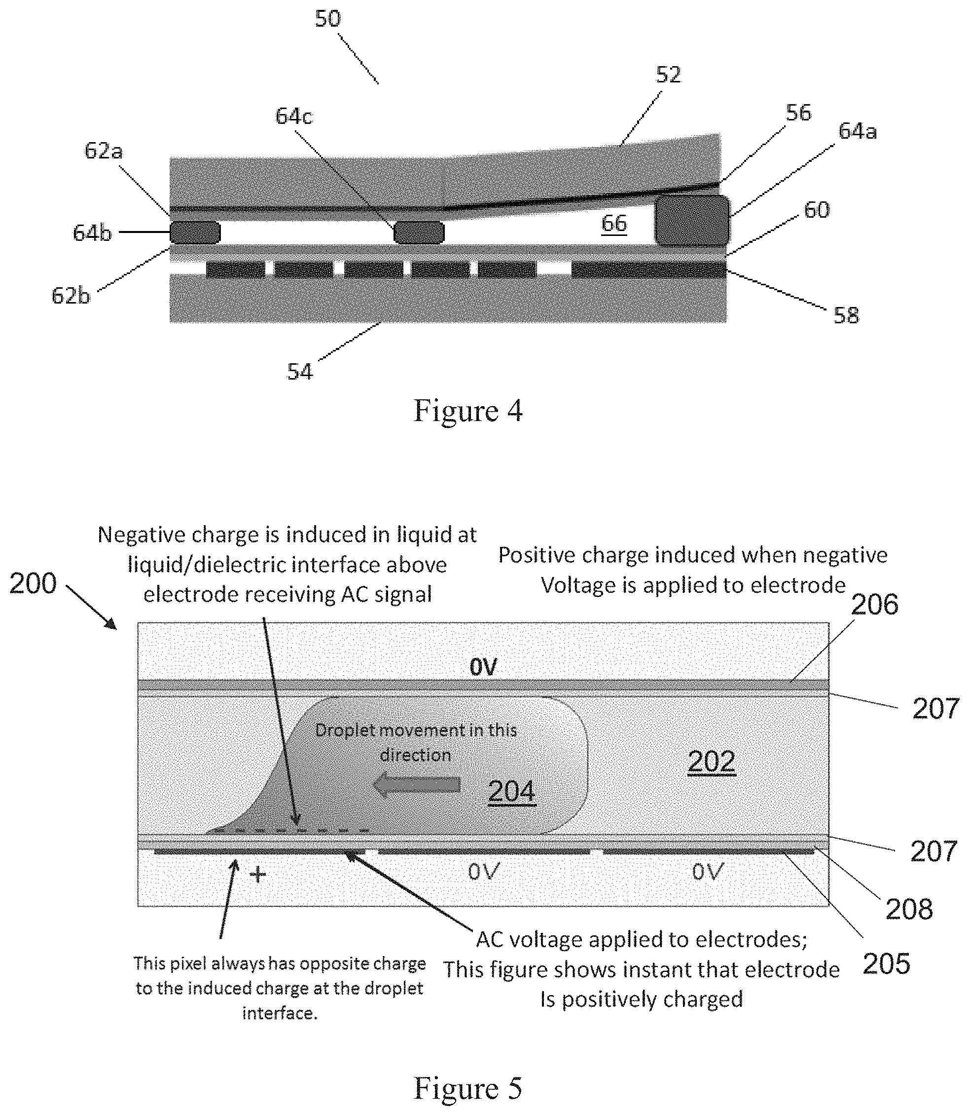
[0004] The fundamental operation of a traditional EWoD device is illustrated in the sectional image of FIG. 5. The EWoD 200 includes a cell filled with an oil 202 and at least one aqueous droplet 204. In a basic configuration, as shown in FIG. 5, a plurality of propulsion electrodes 205 are disposed on one substrate and a singular top electrode 206 is disposed on the opposing surface. The cell additionally includes hydrophobic coatings 207 on the surfaces contacting the oil layer, as well as a dielectric layer 208 between the propulsion electrodes 205 and the hydrophobic coating 207. (The upper substrate may also include a dielectric layer, but it is not shown in FIG. 5). The hydrophobic layer prevents the droplet from wetting the surface. When no voltage differential is applied between adjacent electrodes, the droplet will maintain a spheroidal shape to minimize contact with the hydrophobic surfaces (oil and hydrophobic layer). Because the droplets do not wet the surface, they are less likely to contaminate the surface or interact with other droplets except when that behavior is desired. When a voltage differential is applied between adjacent electrodes, the voltage on one electrode attracts opposite charges in the droplet at the dielectric-to-droplet interface, and the droplet moves toward this electrode.
[0005] As illustrated in FIG. 5, EWoD devices typically comprise two parallel substrates. The operations for moving the droplets within the gap between the two substrates generally fall under one of four main operations: transport (i.e. laterally moving a droplet through the gap), splitting (i.e. dividing a droplet into two or more droplets of lesser volume), dispensing (i.e. extracting a droplet from a large reservoir of fluid), and mixing/merging (i.e. the combination of two droplets into one drop of larger volume). The efficiency of each of the operations is dependent on several factors. For example, the voltages needed for acceptable droplet propulsion depend on the properties of the dielectric and hydrophobic layers. However, another critical factor is the aspect ratio (h/L) of the droplet. The height of the droplet ("h") will equal the gap height between the two parallel substrates because the droplet will span this entire dimension. The length ("L") equals the width or the dimension of the droplet perpendicular to the height. There is an optimal aspect ratio for a droplet depending on the operation to be performed. For example, if the aspect ratio of the droplet within a zone of the device dedicated for a transport operation is too low (i.e. the length of the droplet is too great), a higher driving voltage may be required to move the droplet due to the large contact area between the droplet and the hydrophobic layers. Splitting operations may be impossible to perform for droplets having too high of an aspect ratio (i.e. the length of the droplet is too small). Due to manufacturing constraints, the design of EWoD devices generally have a uniform gap height and include electrodes having uniform dimensions; thereby, providing a limit on the achievable aspect ratios for various regions of the device. Thus, there is a need for improved EWoD devices capable of more efficient droplet propulsion operations and cost-effective methods for their manufacture.
SUMMARY OF INVENTION
[0006] In a first aspect, the present application provides a microfluidic device comprising: (a) top plate, comprising: a top substrate; a first layer of hydrophobic material coupled to a surface of the top substrate; a continuous electrode between the first layer of hydrophobic material and the top substrate; (b) a bottom plate, comprising: a bottom substrate; a plurality of electrodes coupled to the bottom substrate; a second layer of hydrophobic material coupled to the second substrate and atop the plurality of electrodes. The top plate and the bottom plate are placed in a spaced relationship, thereby defining a gap between the first and second layers of hydrophobic material to permit droplet motion within the gap under application of propulsion voltages. At least one of the top substrate, the first layer of hydrophobic material, the second layer of hydrophobic material, the bottom substrate, and the plurality of electrodes has a non-uniform thickness, and the gap has a plurality of heights.
[0007] In a second aspect, the present application provides a method of making a microfluidic device comprising: providing a first substrate and a second substrate, at least one of the first and second substrates having a plurality of thicknesses; applying a first layer of hydrophobic material to a surface of the first substrate, to form a top plate; applying a plurality of electrodes to a surface of the second substrate and a second layer of hydrophobic material on the plurality of electrodes, to form a bottom plate; and placing the bottom plate in a spaced relationship defining a gap between the first and second layers of hydrophobic material to permit droplet motion within the gap under application of propulsion voltages.
[0008] In a third aspect, the present application provides a method of making a microfluidic device comprising: providing a first substrate and a second substrate; applying a first layer of hydrophobic material to a surface of the first substrate, to form a top plate; applying a plurality of electrodes to a surface of the second substrate and a second layer of hydrophobic material on the plurality of electrodes, to form a bottom plate; and placing the bottom plate in a spaced relationship defining a gap having a plurality of heights between the first and second layers of hydrophobic material to permit droplet motion within the gap under application of propulsion voltages.
[0009] These and other aspects of the present invention will be apparent in view of the following description.
BRIEF DESCRIPTION OF DRAWINGS
[0010] The drawing Figures depict one or more implementations in accord with the present concepts, by way of example only, not by way of limitations. The drawings are not to scale. In the figures, like reference numerals refer to the same or similar elements.
[0011] FIG. 1 is a schematic cross-sectional side view of an EWoD device according to a first embodiment of the present invention.
[0012] FIG. 2 is a schematic cross-sectional side view of an EWoD device according to a second embodiment of the present invention.
[0013] FIG. 3 is a schematic cross-sectional side view of an EWoD device according to a third embodiment of the present invention.
[0014] FIG. 4 is a schematic cross-sectional side view of an EWoD device according to a fourth embodiment of the present invention.
[0015] FIG. 5 is a schematic cross-sectional side view of a traditional EWoD device.
DETAILED DESCRIPTION
[0016] In the following detailed description, numerous specific details are set forth by way of examples in order to provide a thorough understanding of the relevant teachings. However, it should be apparent to those skilled in the art that the present teachings may be practiced without such details.
[0017] The various embodiments of the present invention provide an EWoD device including dual substrates. As depicted herein the "bottom" substrate includes a plurality of electrodes to propel various droplets through a microfluidic region. The "top" substrate includes layer of conductive material, which serves as a common conductor. The use of "top" and "bottom" is merely a convention as the locations of the two substrates can be switched, and the devices can be oriented in a variety of ways, for example, the top and bottom substrates can be roughly parallel while the overall device is oriented so that the substrates are normal to a work surface (as opposed to parallel to the work surface as shown in the figures). The top or the bottom substrate may include additional functionality, such as resistive heating and/or temperature sensing. Various materials that may be used to form the top and/or bottom substrate include, but are not limited to, glass and other oxides, semiconductor materials (e.g. silicon), plastics (e.g. acrylics), and combinations thereof.
[0018] The term "coupled", refers to any director indirect structural coupling or connection between two or more parts of a device, where the parts may either be in direct physical contact or coupled through an intermediate part, for example and intermediate layer, member or adhesive. By way of example, a layer "coupled" to a substrate may in certain instances refer to a configuration where the layer is directly adjacent to and in physical contact with the substrate. However, depending on the context, one or more additional layers or other parts may be interposed between the layer and substrate.
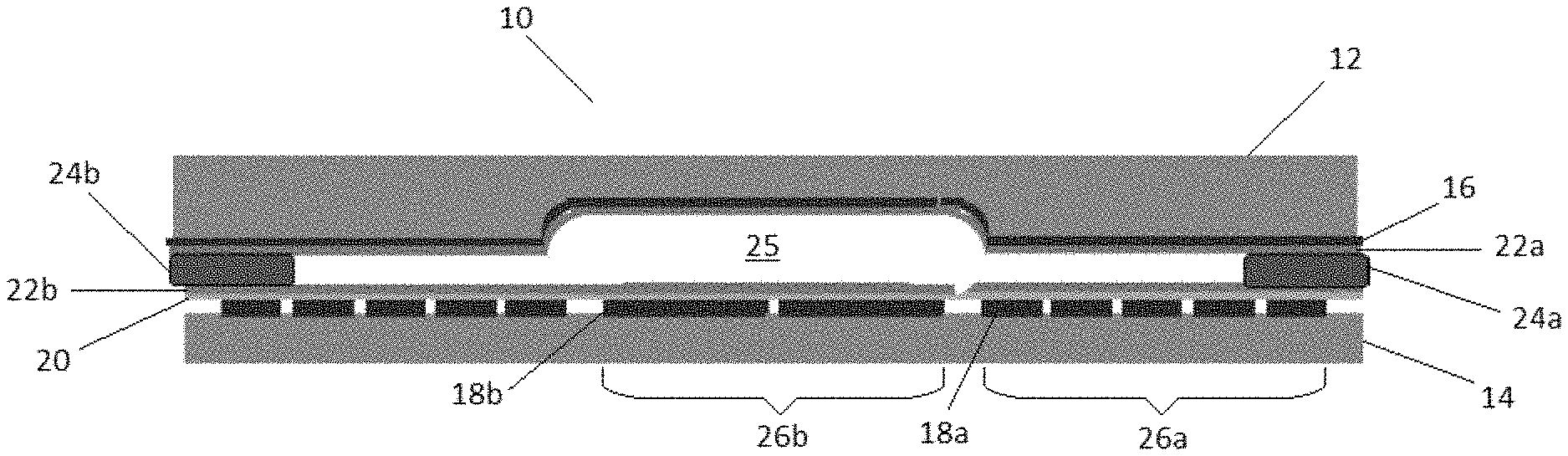
[0019] Referring now to FIG. 1, a microfluidic device 10 comprises a top plate and bottom plate. The top plate includes a top substrate 12, and the bottom plate includes bottom substrate 14. The two plates are generally parallel to each other, as well as being fixed relative to each other. As used herein, "fixed` means that the device 10 does not include any mechanical or electro-mechanical parts that would allow the distance between the top and bottom plates to be variably adjusted. In one embodiment, the top and bottom plates are pressed together to form a reversible attachment. Alternatively, the attachment may be secured with removable or permanent fasteners.
[0020] The top substrate 12 includes an interior surface to which a continuous layer of conductive material 16 may be applied to most, if not all, of the interior surface. A layer of hydrophobic material 22a may then be applied over the continuous electrode 16. The entire area of the continuous electrode 16 is preferably coated with the layer of hydrophobic material 22a. The conductive material of the continuous electrode includes, but is not limited to, metal oxides (e.g. indium tin oxide) and conductive polymers (PEDOT:PSS). The hydrophobic layer 22a may be manufactured from hydrophobic materials formed into coatings by deposition onto a surface via suitable techniques. Depending on the hydrophobic material to be_applied, example deposition techniques include spin coating, molecular vapor deposition, and chemical vapor deposition. Hydrophobic layers may be more or less wettable as usually defined by their respective contact angles. Unless otherwise specified, angles are herein measured in degrees (.degree.) or radians (rad), according to context. For the purpose of measuring the hydrophobicity of a surface, the term "contact angle" is understood to refer to the contact angle of the surface in relation to deionized (DI) water. If water has a contact angle between 0.degree.<.theta.<90.degree., then the surface is classed as hydrophilic, whereas a surface producing a contact angle between 90.degree.<.theta.<180.degree. is considered hydrophobic. Usually, moderate contact angles are considered to fall in the range from about 90.degree. to about 120.degree., while high contact angles are typically considered to fall in the range from about 120.degree. to about 150.degree.. In instances where the contact angle is 150.degree.<.theta. then the surface is commonly known as superhydrophobic or ultrahydrophobic. Surface wettabilities may be measured by analytical methods well known in the art, for instance by dispensing a droplet on the surface and performing contact angle measurements using a contact angle goniometer. Anisotropic hydrophobicity may be examined by tilting substrates with gradient surface wettability along the transverse axis of the pattern and examining the minimal tilting angle that can move a droplet.
[0021] Hydrophobic layers of moderate contact angle typically include one or a blend of fluoropolymers, such as PTFE (polytetrafluoroethylene), FEP (fluorinated ethylene propylene), PVF (polyvinylfluoride), PVDF (polyvinylidene fluoride), PCTFE (polychlorotrifluoroethylene), PFA (perfluoroalkoxy polymer), FEP (fluorinated ethylenepropylene), ETFE (polyethylenetetrafluoroethylene), and ECTFE (polyethylenechlorotrifluoroethylene). Commercially available fluoropolymers include Cytop.RTM. (AGC Chemicals, Exton, Pa.) and Teflon.RTM. AF (Chemours, Wilmington, Del.). An advantage of fluoropolymer films is that they can be highly inert and can remain hydrophobic even after exposure to oxidizing treatments such as corona treatment and plasma oxidation.
[0022] The bottom substrate 14 has an interior surface to which a plurality of electrodes 18a, 18b may be applied. The electrodes may be a passive matrix or an active matrix, such as a TFT array. A layer of dielectric material 20 is coated over the plurality of electrodes, preferably over the entire area of the electrodes, as well as a layer of hydrophobic material 22b that may the same or similar to the composition of the hydrophobic material layer 22a applied to the top substrate. The dielectric layer may comprise a layer of approximately 20-40 nm SiO.sub.2 topped over-coated with 200-400 nm plasma-deposited silicon nitride. Alternatively, the dielectric may comprise atomic-layer-deposited Al.sub.2O.sub.3 between 2 and 100 nm thick, preferably between 20 and 60 nm thick. While it is possible to have a single layer for both the dielectric and hydrophobic functions, such layers typically require thick inorganic layers (to prevent pinholes) with resulting low dielectric constants, thereby requiring more than 100V for droplet movement. To achieve low voltage actuation, it is better to have a thin dielectric inorganic layer for high capacitance and to be pinhole free, topped by a thin organic hydrophobic layer. With this combination it is possible to have electrowetting operation with voltages in the range +/-10 to +/-50V, which is in the range that can be supplied by conventional TFT arrays. AC driving is used to reduce degradation of the droplets, dielectrics, and electrodes by various electrochemistries. Operational frequencies for EWoD can be in the range 100 Hz to 1 MHz, but lower frequencies of 1 kHz or lower are preferred for use with TFTs that have limited speed of operation. Examples of various architectures for the electrodes and driving methods are disclosed in U.S. patent application Ser. No. 16/161,548, the entire content of which is incorporated by reference herein.
[0023] As previously mentioned, the top plate and bottom plate may fixed relative to each other, for example by pressing together until a reversible attachment is established. The distance and separation between the top plate and bottom plate may be maintained by one or more spacers 24a, 24b in order to provide a gap 25 between the substrates 12, 14. The gap 25 is preferably filled with a gap fluid. The droplet samples propelled within the device should not be miscible in the gap fluid. For example, if the microfluidic device is used to perform analyses on aqueous droplet samples, it is usually preferred that the gap fluid is a hydrophobic fluid, such as silicone oil, dodecane, or other long-chain, non-polar hydrocarbon oils.
[0024] As illustrated in FIG. 1, the top substrate 12 does not have a uniform thickness. Instead, the thickness of the top substrate 12 within one cross-sectional area 26b may be less than the thickness of the top substrate 12 within an adjacent cross-sectional area 26a. As a result, the height of the gap 25 in area 26a is less than the gap height in area 26b. Each of the areas 26a, 26b may be an operation-specific zone. For example, area 26a having a small gap height may be an operation-specific zone dedicated to a splitting operation, while the area 26b having the larger gap height may be a transport zone. Each operation-specific zone (e.g. transport zone, dispensing zone, splitting zone, and mixing zone) may have a gap height that is different than the gap height of at least one of the other operation-specific zones. Each gap height is typically in the range 50 to 200 .mu.m, but the gap can be larger.
[0025] In order to provide the top substrate 12 with a non-uniform thickness, the top substrate 12 may be made from an etchable material, such as glass. An etching process, such as a wet etching process, may be performed by first applying a resist to a surface of a glass substrate in a desired pattern. The patterned surface may then be exposed to a chemical etchant for a specified amount of time in order to remove a portion of the exposed glass. After a sufficient amount of material has been chemically etched away, the patterned surface may be washed to remove the resist and any residual etchant. Dry etching processes (e.g. plasma or photo-induced etching) may also be used to provide the top substrate with a non-uniform thickness.
[0026] In another method according to an embodiment of the present invention, one or both substrates of the microfluidic device may be molded or formed to provide a non-uniform surface. For example, a stamp having an inverse of the desired pattern for the surface of the substrate may be applied to one or both substrates, preferably prior to the application of any of the additional layers. Another method of providing one of the substrates with a non-uniform thickness would be by embossing. For example, the substrate may be made of an embossable material, such as a plastic film, and an embossing roller having an inverse of the desired pattern may be applied to the surface of the substrate material. The embossing process may be a roll-to-roll processes, such as those described in U.S. Pat. No. 6,930,818, the entire content of which is incorporated by reference herein. Embossing procedures may be used to provide the surface of the substrate with the desired surface topography after being coated (e.g. after the top substrate is coated with a layer of conductive material or the layer of hydrophobic material). However, it is preferred that the embossing is performed prior to application of these layers.
[0027] In some embodiments, both the top and bottom substrate may be provided with non-uniform thicknesses; however, providing the bottom substrate with a non-uniform surface topography is less preferred because applying an array of electrodes to a non-uniform surface may be more difficult and therefore, more costly, than coating a continuous layer of conductive material to a non-uniform surface on the top substrate. Therefore, it is preferred that of the two substrates, only the substrate carrying the continuous conductor is provided with a surface topography. In another aspect of the present invention, the top substrate may be changed with another top substrate having a different surface topography. Therefore, various embodiments of the present invention may be provided in the form of a kit comprising a bottom substrate and a plurality of top substrates each having a different surface topography that are configured to be releasably attached to the bottom substrate, such as with fasteners. This would allow the user to select from various top substrate options depending on the desired operations to be performed within the microfluidic device.
[0028] As illustrated in FIG. 1, the electrodes on the bottom substrate 14 within one cross-sectional area 26a may have a shorter side length than the electrodes on the bottom substrate 14 within another cross-sectional area 26b. Therefore, devices made according to one embodiment of the invention may have a specific electrode width depending on the gap height 25 of the cross-sectional area in which the electrode is located. This may provide more control over how a desired aspect ratio may be achieved for a droplet within certain areas of the device 10. Due to the difficulty of forming an array of electrodes having varying sizes, it is preferred to provide the bottom substrate 14 with an array of substantially uniform side lengths. For microfluidic devices having an array of similarly sized driving electrodes, the cross-sectional areas in which a larger electrode side length is desired may be achieved by ganging a group of electrodes together, such that the gang of electrodes to operate in unison. Generally, an aspect ratio of approximately 1:2, more preferably about 1:3, should be maintained for effective performance of each propulsion operation. Therefore, the width of the droplet formed by the electrode or gang of electrodes should be approximately three times greater than the height.
[0029] As an alternative to removing or etching material, a microfluidic device with a gap having a plurality of heights according to various embodiments of the present invention may be made by applying a pattern of additive material to an interior surface of one or both substrates. For example referring to FIG. 2, a microfluidic device 30 is illustrated having the same features as the previously described embodiment. The top plate of device 30 may comprise a top substrate 32 having a layer of conductive material forming a continuous electrode 38 and a layer of hydrophobic material 42a applied to an internal surface of the top substrate 32, as well as a bottom plate comprising bottom substrate 34, plurality of electrodes 40, a dielectric layer 41, and a layer of hydrophobic material 42b also applied to an internal surface. One or more spacers 44a, 44b maintain the top and bottom substrates 32, 34 apart to provide a gap 45 between the layers of hydrophobic material 42a, 42b. The embodiment illustrated in FIG. 2 differs from the previously described embodiment in that the top and bottom substrates 32, 34 have a substantially uniform thickness, but an additive material 36 has been applied in specific locations on the interior surface of the top substrate 32 to reduce the height of the gap 45 that is adjacent to the additive material 36.
[0030] In some embodiments, the additive material may be the same material as the conductive material or the hydrophobic material. However, with respect to the top substrate 32, it is less preferred that the additive material 36 is the same material as the conductive material of the continuous electrode 38 because a layer of conductive material having a non-uniform thickness may cause a variation in electrical properties across the device 30. The additive material 36 may be applied to the substrate either before or after application of the layer of conductive material 38, preferably before. If the additive material 36 is not hydrophobic, it is also preferred that the additive material 36 is applied prior to the layer of hydrophobic material 42a. The additive material 36 may also be patterned onto the interior surface of the bottom substrate 34 or over the plurality of electrodes 40. Using a pattern of dielectric material 41 to provide the surface topography however is a less preferred option, as it may cause non-uniform electrical properties across the interior surface of the bottom substrate 34. Types of additive materials that may be used to form the surface topography of the substrates include, but are not limited to, photoresist materials (e.g. SU-8), polymeric materials (e.g. PMMA), and dielectric materials (e.g. inorganic oxides).
[0031] It may be desired in some applications for the microfluidic device made according to the various embodiments of the present invention to have a light transmissive top substrate and/or bottom substrate, as well as the layers applied thereto, to perform certain analytical procedures on the droplet samples within the gap of the device. For example, fluorescent markers may be observed by illuminating a droplet through the top substrate with a light source and then using a detector and optionally colored filters to observe the resulting fluorescence through the top substrate. In other embodiments, the light may pass through both the top and bottom substrates to allow absorption measurements in the IR, UV, or visible wavelengths. Alternatively, attenuated (frustrated) total-internal reflection spectroscopy can be used to probe the contents and or location of droplets in the system.
[0032] There is no limitation as to how the pattern of the additive material may be formed on the surface of one of the substrates of the microfluidic device. For example if the additive material comprises hydrophobic material, an initial uniform coating of hydrophobic material may be applied to the conductive layer followed by a pattern of additional hydrophobic material or vice versa. In another method, one or more stencils or masks having the desired pattern may be applied to the substrate prior to coating the surface of the substrate with the additive material. The mask may then be lifted to reveal the desired pattern. If multiple masks are used, the coating of additive material is preferably dried between applications. Once the pattern is formed, the layer of conductive material and hydrophobic material may be applied over the patterned additive material. In another method, a uniform layer of additive material may be applied over the entire surface of a substrate. A laser may be used to etch the additive material to form the surface topography. Alternatively, one or more masks or a resist may be applied in a pattern to a uniform coating of additive material prior to the removal of any exposed material using a chemical etchant. Again, the layer of conductive material and hydrophobic material may be applied over the additive material after etching and rinsing the surface pattern.
[0033] As previously noted, the top and/or bottom substrates may be modified to include additive material to provide a device with a plurality of gap heights. For example, as illustrated in FIG. 3, a less preferred embodiment of the present invention is illustrated. A microfluidic device 31 includes an array of short electrodes 40a and tall electrodes 40b on the bottom substrate 34. Additional conductive material is used to form the tall electrodes 40b and thereby decrease the height of the gap 45 adjacent to the tall electrodes 40b relative to the gap height adjacent to the short electrodes 40a.
[0034] Referring now to FIG. 4, a microfluidic device 50 may be formed by applying a plurality of spacers 64a, 64b, 64c having various heights to the bottom substrate 54 after application of a dielectric material 60 and hydrophobic layer 62b. A top substrate 52 having a common electrode layer 56 and hydrophobic layer 62a may then be pressed and bonded onto the plurality of spacers 64a, 64b, 64c, such that the varying heights of the gap 66 are maintained by the spacers 64a, 64b, 64c and the gap heights in any location within the device 50 are dependent on the dimensions of the spacers 64a, 64b, 64c in the vicinity of the gap 66. In each of the deformation processes, heat and/or pressure may be used to provide a more pliable and deformable substrate and to facilitate bonding of the top substrate to the spacers.
[0035] From the foregoing, it will be seen that the present invention provides improved methods of fabricating devices to allow for greater design selection in gap height at specific regions of the device to match electrode dimensions for greater effective of control over the propulsion operations of the same droplets within the microfluidic device. For example, a customized gap height at the location of reagent input reservoirs change the friction and capillary forces for dispensing droplets into the device. Larger gap heights create a more favorable capillary action. Smaller gap heights with smaller electrodes may enable improved volume control of droplets. Some operations may also be improved, such as mixing wherein the droplet may be moved from an area with a large gap height to an area with a smaller gap height. Smaller effective gap heights may also enable the use of less reagent volumes. Reagents for some analyses are very expensive, so the ability to perform reactions and operations effectively with reduced reagent volumes offers potential cost advantages.
[0036] While preferred embodiments of the invention have been shown and described herein, it will be understood that such embodiments are provided by way of example only. Numerous variations, changes, and substitutions will occur to those skilled in the art without departing from the spirit of the invention. Accordingly, it is intended that the appended claims cover all such variations as fall within the spirit and scope of the invention.
[0037] All of the contents of the aforementioned patents and applications are incorporated by reference herein in their entireties. In the event of any inconsistency between the content of this application and any of the patents and application incorporated by reference herein, the content of this application shall control to the extent necessary to resolve such inconsistency.
* * * * *
D00000
D00001
D00002
XML
uspto.report is an independent third-party trademark research tool that is not affiliated, endorsed, or sponsored by the United States Patent and Trademark Office (USPTO) or any other governmental organization. The information provided by uspto.report is based on publicly available data at the time of writing and is intended for informational purposes only.
While we strive to provide accurate and up-to-date information, we do not guarantee the accuracy, completeness, reliability, or suitability of the information displayed on this site. The use of this site is at your own risk. Any reliance you place on such information is therefore strictly at your own risk.
All official trademark data, including owner information, should be verified by visiting the official USPTO website at www.uspto.gov. This site is not intended to replace professional legal advice and should not be used as a substitute for consulting with a legal professional who is knowledgeable about trademark law.