Selective Deposition Of Tungsten
Kovalgin; Alexey Y. ; et al.
U.S. patent application number 16/926192 was filed with the patent office on 2020-10-29 for selective deposition of tungsten. The applicant listed for this patent is ASM IP Holding B.V.. Invention is credited to Antonius A. I. Aarnink, Alexey Y. Kovalgin, Rob A.M. Wolters, Mengdi Yang.
| Application Number | 20200343134 16/926192 |
| Document ID | / |
| Family ID | 1000004946122 |
| Filed Date | 2020-10-29 |


View All Diagrams
| United States Patent Application | 20200343134 |
| Kind Code | A1 |
| Kovalgin; Alexey Y. ; et al. | October 29, 2020 |
SELECTIVE DEPOSITION OF TUNGSTEN
Abstract
A method for selectively depositing a metal film onto a substrate is disclosed. In particular, the method comprising flowing a metal precursor onto the substrate and flowing a non-metal precursor onto the substrate, while contacting the non-metal precursor with a hot wire. Specifically, a reaction between a tungsten precursor and a hydrogen precursor selectively forms a tungsten film, where the hydrogen precursor is excited by a tungsten hot wire.
| Inventors: | Kovalgin; Alexey Y.; (Enschede, NL) ; Yang; Mengdi; (Enschede, NL) ; Aarnink; Antonius A. I.; (Enschede, NL) ; Wolters; Rob A.M.; (Enschede, NL) | ||||||||||
| Applicant: |
|
||||||||||
|---|---|---|---|---|---|---|---|---|---|---|---|
| Family ID: | 1000004946122 | ||||||||||
| Appl. No.: | 16/926192 | ||||||||||
| Filed: | July 10, 2020 |
Related U.S. Patent Documents
| Application Number | Filing Date | Patent Number | ||
|---|---|---|---|---|
| 15615489 | Jun 6, 2017 | 10714385 | ||
| 16926192 | ||||
| 62364185 | Jul 19, 2016 | |||
| 62414408 | Oct 28, 2016 | |||
| Current U.S. Class: | 1/1 |
| Current CPC Class: | C23C 16/45553 20130101; C23C 16/45536 20130101; H01L 21/28562 20130101; C23C 16/045 20130101; H01L 21/76843 20130101; C23C 16/06 20130101; C23C 16/14 20130101; H01L 21/76849 20130101; H01L 23/53238 20130101; C23C 16/04 20130101; C23C 16/56 20130101 |
| International Class: | H01L 21/768 20060101 H01L021/768; C23C 16/04 20060101 C23C016/04; C23C 16/14 20060101 C23C016/14; C23C 16/56 20060101 C23C016/56; C23C 16/455 20060101 C23C016/455; C23C 16/06 20060101 C23C016/06; H01L 21/285 20060101 H01L021/285; H01L 23/532 20060101 H01L023/532 |
Claims
1. A method of selectively forming a film comprising metal, the method comprising: providing a substrate for processing in a reaction chamber and a hot wire element for contacting at least a gas; exposing the substrate to a metal precursor; and exposing the substrate to a gas which has been exposed to a vicinity of the hot wire; wherein the substrate comprises at least two different materials and the metal film is selectively formed in one of the surfaces.
2. The method of claim 1, wherein the metal precursor comprises transition metal element.
3. The method of claim 1, wherein the metal precursor comprises a tungsten-containing precursor or a molybdenum-containing precursor.
4. The method of claim 1, wherein the gas comprises hydrogen.
5. The method of claim 1, wherein the selectively formed film comprises metallic material.
6. The method of claim 1, wherein an excited, radical or atomic species is formed from the gas when the gas has been exposed to a vicinity of the hot wire.
7. The method of claim 1, wherein the substrate comprises a first surface and a second surface.
8. The method of claim 7, wherein the first surface comprises a transition metal.
9. The method of claim 7, wherein the first surface comprises an oxidized metal, and underneath the oxidized metal is an elemental metal or metallic conductive film.
10. The method of claim 7, wherein the second surface comprises Si--O bonds.
11. The method of claim 7, wherein the second surface comprise silicon oxide, silicon nitride, silicon carbide, silicon oxynitride, silicon dioxide, or mixtures thereof
12. The method of claim 7, wherein the film is selectively formed on the first surface.
13. The method of claim 1, further comprising the step of exposing the substrate to a purge gas after the steps of exposing the substrate to the metal precursor.
14. The method of claim 1, wherein a selectivity is above 50%.
15. The method of claim 1, wherein the thickness of the film as above 1 nm.
16. The method of claim 1, wherein a wall in the reaction chamber is a hot wall.
17. The method of claim 1, wherein selectively forming the film comprises an ALD process.
18. The method of claim 1, wherein selectively forming the film comprises a cyclic process.
19. The method of claim 1, wherein selectively forming the film comprises cyclic or sequential CVD process.
20. A reaction chamber, configured to perform the method of claim 1.
Description
CROSS-REFERENCE TO RELATED PATENT APPLICATIONS
[0001] This application is a continuation and claims priority to U.S. patent application Ser. No. 15/615,489, filed Jun. 6, 2017, entitled SELECTIVE DEPOSITION OF TUNGSTEN; which claims the benefit of U.S. Provisional Patent Application No. 62/364,185, filed on Jul. 19, 2016 entitled "SELECTIVE DEPOSITION OF TUNGSTEN," and of U.S. Provisional Patent Application No. 62/414,408, filed on Oct. 28, 2016 entitled "SELECTIVE DEPOSITION OF TUNGSTEN," the disclosures of which are hereby incorporated by reference in their entirety.
FIELD OF INVENTION
[0002] The present disclosure generally relates to processes for manufacturing electronic devices. More particularly, the disclosure relates to selective deposition through cyclic exposure or atomic layer deposition (ALD) with a hot wire system. Specifically, the disclosure relates to forming tungsten films through a hot wire cyclic exposure process.
BACKGROUND OF THE DISCLOSURE
[0003] Processes exist to selectively deposit tungsten utilizing disilane (Si.sub.2H.sub.6) and tungsten hexafluoride (WF.sub.6) as precursors. U.S. Pat. No. 8,956,971 to Haukka et al. discloses such a process, where the deposition takes place at approximately a temperature of 150.degree. C. The deposition may result in a tungsten layer being formed over a copper surface.
[0004] Approaches to form tungsten via plasma have not been viable due to plasma's adverse effect on the selectivity. Specifically, plasma tends to form films on multiple surfaces, and does not discriminate between the different surfaces.
[0005] Formation of tungsten films may be used to improve electromigration (EM) resistance. The EM resistance may be achieved by forming a metal cap over an interface between a dielectric diffusion barrier and a metallic material. However, achieving good selectivity on metallic surfaces versus the dielectric surface has been difficult. Several approaches have been taken, such as gentle surface treatments comprising thermal or radical treatments, in order to obtain the desired surface terminations. The gentle surface treatments, however, may not adequately prepare the desired surface for selective deposition.
[0006] As a result, a process is desired that deposits a tungsten or other metal film with a high selectivity.
SUMMARY OF THE DISCLOSURE
[0007] In accordance with at least one embodiment of the invention, a method of selectively forming a tungsten film is disclosed. The method comprises: providing a substrate comprising a first surface and a second surface for processing in a reaction chamber and a hot wire for creating an excited species of a gas; performing a tungsten precursor pulse/purge step onto the substrate, comprising: pulsing a tungsten precursor onto the substrate; and purging an excess of the tungsten precursor from the reaction chamber; and performing a hydrogen precursor pulse/purge step onto the substrate, comprising: pulsing a hydrogen precursor onto the substrate, wherein the hydrogen precursor is excited by the hot wire; and purging an excess of the hydrogen precursor from the reaction chamber; wherein the tungsten precursor comprises at least one of: tungsten hexafluoride (WF.sub.6); wherein the hydrogen precursor comprises at least one of: hydrogen (H.sub.2); wherein a temperature of the hot wire is above about 1000.degree. C.; and wherein a tungsten film is selectively formed on the first surface.
[0008] In accordance with at least one embodiment of the invention, a method of selectively forming a film comprising metal is disclosed. The method comprises: providing a substrate for processing in a reaction chamber and a hot wire element for contacting at least a gas; exposing the substrate to a metal precursor; and exposing the substrate to a gas which has been exposed to a vicinity of the hot wire; wherein the substrate comprises at least two different materials and the metal film is selectively formed in one of the surfaces.
[0009] In accordance with at least one embodiment of the invention, a method of forming a tungsten film is disclosed. The method comprises: providing a substrate for processing in a reaction chamber and a hot wire for passing at least a gas through to the reaction chamber; flowing a tungsten precursor onto the substrate; and flowing a hydrogen precursor onto the substrate, wherein the hydrogen precursor is contacted with the hot wire; and wherein a reaction between the tungsten precursor and the hydrogen precursor contacted with the hot wire forms a tungsten film; and wherein the reaction chamber is a hot-wall reaction chamber.
[0010] For purposes of summarizing the invention and the advantages achieved, certain objects and advantages of the invention have been described herein above. Of course, it is to be understood that not necessarily all such objects or advantages may be achieved in accordance with any particular embodiment of the invention. Thus, for example, those skilled in the art will recognize that the invention may be embodied or carried out in a manner that achieves or optimizes one advantage or group of advantages as taught or suggested herein without necessarily achieving other objects or advantages as may be taught or suggested herein.
[0011] All of these embodiments are intended to be within the scope of the invention herein disclosed. These and other embodiments will become readily apparent to those skilled in the art from the following detailed description of certain embodiments having reference to the attached figures, the invention not being limited to any particular embodiment(s) disclosed.
BRIEF DESCRIPTION OF THE DRAWING FIGURES
[0012] These and other features, aspects, and advantages of the invention disclosed herein are described below with reference to the drawings of certain embodiments, which are intended to illustrate and not to limit the invention.
[0013] FIG. 1 illustrates a method in accordance with at least one embodiment of the invention.
[0014] FIG. 2 illustrates a method in accordance with at least one embodiment of the invention.
[0015] FIG. 3 illustrates a method step in accordance with at least one embodiment of the invention.
[0016] FIG. 4 illustrates a method step in accordance with at least one embodiment of the invention.
[0017] FIGS. 5A and 5B illustrate a top view of a structure in accordance with at least one embodiment of the invention.
[0018] FIGS. 6A and 6B illustrate a cross-sectional view of a structure in accordance with at least one embodiment of the invention.
[0019] FIG. 7 illustrates a method in accordance with at least one embodiment of the invention.
[0020] FIG. 8 illustrates a method in accordance with at least one embodiment of the invention.
[0021] FIG. 9 illustrates a method in accordance with at least one embodiment of the invention.
[0022] FIG. 10 illustrates a cross-sectional view of a structure in accordance with at least one embodiment of the invention.
[0023] FIG. 11 illustrates a cross-sectional view of a structure in accordance with at least one embodiment of the invention.
DETAILED DESCRIPTION OF EXEMPLARY EMBODIMENTS
[0024] Although certain embodiments and examples are disclosed below, it will be understood by those in the art that the invention extends beyond the specifically disclosed embodiments and/or uses of the invention and obvious modifications and equivalents thereof. Thus, it is intended that the scope of the invention disclosed should not be limited by the particular disclosed embodiments described below.
[0025] Deposition of a film may take place using an apparatus utilizing a hot wire or a heating filament to generate a radical species from a flowed precursor gas flowing alongside and in close proximity to the hot wire. Such an apparatus is disclosed in U.S. Patent Application Publication No. 2013/0337653 A1, which is incorporated by reference. Other heating filaments are disclosed in U.S. Patent Application Publication No. 2014/0120723 A1. The apparatus may include a reaction chamber, a substrate holder, a gas source, and a hot wire or heating filament for generating radicals from a gas flowing along the hot wire, a heater for heating the substrate holder and a heater for heating the walls of the reaction chamber.
[0026] Within the reaction chamber, a substrate holder is disposed to hold a substrate. A gas source may provide a precursor gas into the reaction chamber. Also within the reaction chamber, there may be the hot wire or heating filament. The hot wire or heating filament may comprise a wire, a ribbon, or a similar structure wound into a coil such that it includes a plurality of windings extending helically around a central, longitudinal axis. The hot wire or heating filament may comprise metal, such as tungsten or other suitable material capable of withstanding temperatures above 1000.degree. C., above 1200.degree. C., above 1300.degree. C., or above 1500.degree. C. In accordance with at least one embodiment, a flowed gas may come into direct contact with the hot wire or heating filament, which catalyzes the process by cracking the flowed gas.
[0027] The precursor gas may come into contact with the hot wire or heating filament, and then dissociate to form a precursor gas radicals, which then may either adsorb onto the substrate or react with an adsorbed precursor on the substrate.
[0028] The substrate may comprise various types of materials. When manufacturing integrated circuits, the substrate typically comprises a number of thin films with varying chemical and physical properties. For example and without limitation, the substrate may comprise a silicon-containing layer and a metal layer. In some embodiments, the substrate can comprise metal carbide. In some embodiments, the substrate can comprise a conductive oxide. In some embodiments, the substrate is a semiconductor wafer comprising silicon and having diameter from about 100 mm to about 450 mm, from about 200 to about 300 mm. In other embodiments the substrate may comprise other types of substrates, such as: glass; semiconductors; like-compound semiconductors, for example III-V or II-VI semiconductors; oxides; and various other types of substrates, such as non-planar or planar substrates.
[0029] In at least one embodiment, the substrate may have a first surface comprising a metal, referred to herein as the first metal surface or first metallic surface. The first surface may be essentially an elemental metal, such as Cu or Co. In other embodiments, the first surface may comprise a metal nitride or a transition metal. The transition metal may be selected from the group: Ti, V, Cr, Mn, Nb, Mo, Ru, Rh, Pd, Ag, Au, Hf, Ta, W, Re, Os, Ir and Pt. In some embodiments, the first surface may comprise a noble metal, such as Au, Pt, Ir, Pd, Os, Ag, Re, Rh, and Ru, for example. In other embodiments, the metal film may be selectively deposited on a metal oxide surface relative to other surfaces, where the metal oxide surface may be, for example, a WO.sub.x, HfO.sub.x, TiO.sub.x, AlO.sub.x, or ZrO.sub.x surface. In some embodiments, a metal oxide surface may be an oxidized surface of a metallic material.
[0030] In at least one embodiment, the substrate may have a second surface, which is preferably a silicon-containing surface, referred to herein as the second silicon-containing surface or second surface comprising silicon. In some embodiments, the silicon-containing surface may comprise, for example, SiO.sub.2. In some embodiments, the silicon-containing surface may comprise material having Si--O bonds, for example, SiO.sub.2 or SiO.sub.2 based low-k material. In some embodiments, the second surface may comprise silicon oxide, silicon nitride, silicon carbide, silicon oxynitride, silicon dioxide, or mixtures thereof. In some embodiments, the material comprising the second surface may be a porous material. In some embodiments, the porous material may contain pores, which are connected to each other, while in other embodiments, the pores are not connected to each other. In some embodiments, the second surface may comprise a low-k material, defined as an insulator with a dielectric value or relative permittivity below about 4.0. In some embodiments, the dielectric value or relative permittivity of the low-k material may be below about 3.5, below about 3.0, below about 2.5, or below about 2.3.
[0031] Embodiments of the invention may be directed to selectively forming metallic films, films comprising transition metals, or metallic films comprising transition metals. In some embodiments, the films could comprise a metal or metallic film comprising Group IV, V, or VI elements of the periodic table of elements. In some embodiments, the films could comprise a metal or metallic film comprising Group V or VI elements of the periodic table of elements. In some embodiments, the films could comprise a metal or metallic film comprising Group VI elements of the periodic table of elements. In some embodiments, the films could be films comprising tungsten or molybdenum. Embodiments of the invention may result in formation of tungsten or molybdenum. In some embodiments, the films formed have resistivity of less than about 200, about 100, less than about 50, less than about 30, less than about 20, or less than about 15 .mu..OMEGA.cm. Typically when the film is thinner, the resistivity may be higher than for bulk film or material; for example, films with thickness of less than 5 nm might exhibit resistivity of less than about 200 .mu..OMEGA.cm, while thicker films with the same deposition process and conditions might exhibit resistivity of less than about 20 .mu..OMEGA.cm. For example, embodiments of the invention may involve reactions of a tungsten precursor with precursor comprising reducing reactant, such as precursor comprising hydrogen, for example a hydrogen precursor. In such an embodiment, a tungsten precursor of tungsten hexafluoride (WF6) may react with a hydrogen precursor comprising hydrogen species, such as excited species of hydrogen or atomic hydrogen in the following reaction:
WF.sub.6+6H.fwdarw.W+6HF
In at least one embodiment, the hydrogen may be atomic species or may become an excited or chemically activated species when exposed to the hot wire.
[0032] Embodiments of the invention may be directed to selectively deposit metal on micrometer-scale (or smaller) features during integrated circuit fabrication. For example, process flows described herein may be used to manufacture features having a size less than 100 micrometers, less than 1 micrometer, or less than 200 nm. In the case of selective deposition of tungsten on copper for interconnects, the size of the feature or line width may be less than 1 micrometer, less than 200 nm, less than 100 nm, or less than 50 nm or less than 30 nm or less than 20nm. One of ordinary skill in the art may recognize that selective deposition on larger features or smaller features and in other contexts is possible using the disclosed methods.
[0033] FIG. 1 illustrates a method in accordance with at least one embodiment of the invention. The method comprises a metal precursor flow step 100 and a non-metal flow step 200, both of which may comprise a purging step. The non-metal flow step 200 may occur such that a non-metal precursor either contacts or is in close proximity to a hot wire. Each of these steps may be repeated via a first path 300 and a second path 310 as needed. The entire cycle may be repeated via a third path 320 as needed. The steps may be repeated in order to form a tungsten film of a desired thickness.
[0034] The method may take place at the following conditions. The pressure in the reaction chamber may range between about 0.001 mbar and about 1000 mbar, between 0.01 about mbar and about 100 mbar, or between about 0.05 mbar and 20 mbar. The substrate temperature may range between about 0 and about 800.degree. C., between about 20 and about 500.degree. C., between about 50 and about 450.degree. C., between about 100 and about 400.degree. C., between about 150 and about 350.degree. C., or between about 250 and about 300.degree. C., or about 275.degree. C. The substrate temperature may be maintained by a heater of a substrate holder. A hot wire temperature may range above about 1000.degree. C., between about 1000 and about 2500.degree. C., between about 1100 and about 2000.degree. C., between about 1200 and about 1900.degree. C., or between 1700 and 1800.degree. C., or about 1750.degree. C.
[0035] In addition, a wall in the reaction chamber may either be a hot wall or a cold wall. A hot wall reactor may be possible in smaller volume reactors, but also for bigger volume reactors, such as batch furnace reactors. On the other hand, a cold wall reactor may be possible for a large volume reactor on the order of tens of liters in volume, but cold wall reactor also may be a small volume reactor, such as a showerhead reactor designed to have small volume and/or possibly a reactor having a cooling system in the upper part of the reaction chamber. In a hot wall reactor, a wafer may be placed in a chamber where both a wafer holder and a cover placed above the wafer are heated or in a reactor in which all of reaction chamber parts and/or walls at equal or close to the temperature of the substrate. For a hot wall, a temperature difference (positive or negative) of one or more of the reaction chamber wall and substrate may be less than about 100.degree. C., may be less than about 50.degree. C., may be less than about 25.degree. C., may be less than about 5.degree. C., or may be about 0.degree. C., and may be maintained by a separate heater. For a cold wall, temperature difference of one or more of the reaction chamber wall (cooler than the substrate) and substrate (hotter than the chamber walls) may be above about 25.degree. C., above about 50.degree. C., above about 75.degree. C., or above about 100.degree. C.
[0036] FIG. 2 illustrates a method in accordance with at least one embodiment of the invention. The method is the same as that displayed in FIG. 1, with the difference that a non-metal precursor flow step 200 precedes a metal precursor flow step 100, both of which may comprise a purging step. Each of these steps may be repeated via a first path 300 and a second path 310 as needed. The entire cycle may be repeated via a third path 320 as needed. The steps may be repeated in order to form a metal film of a desired thickness. The metal film may comprise at least one of: a transition metal; a metallic material; an elemental transition metal film; elemental tungsten; elemental molybdenum.
[0037] The method may take place at the following conditions. The pressure in the reaction chamber may range between about 0.001 mbar and about 1000 mbar, between 0.01 about mbar and about 100 mbar, or between about 0.05 mbar and 20 mbar or in some instances about 0.05 mbar. The substrate temperature may range between about 0 and about 800.degree. C., between about 20 and about 500.degree. C., between about 50 and about 450.degree. C., between about 100 and about 400 .degree. C., between about 150 and about 350.degree. C., or between about 250 and about 300.degree. C., and may be maintained by a heater of a substrate holder. A hot wire temperature may range above about 1000 .degree. C., between about 1000 and about 2500.degree. C., between about 1100 and about 2000.degree. C., between about 1200 and about 1900.degree. C., or between 1700 and 1750.degree. C.
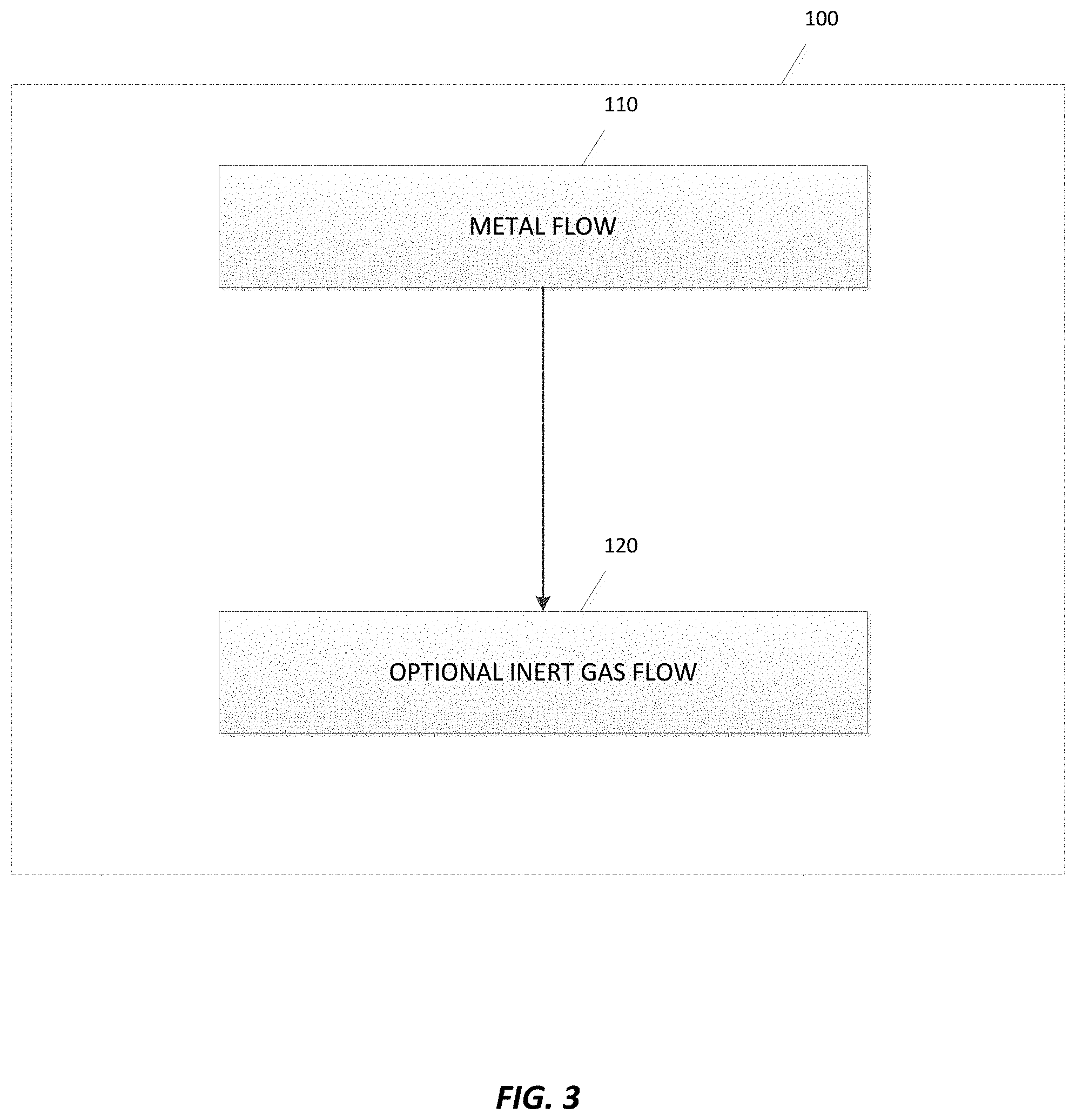
[0038] FIG. 3 illustrates the metal precursor flow step 100, which comprises a metal flow 110 and an optional inert gas flow 120. The metal flow 110 involves a flow, exposure, or a pulse of a metal precursor. The metal precursor may comprise at least one of: a transition metal element; a Group IV element; a Group V element; a Group VI element; Tungsten-containing precursor; a transition metal halide; a transition metal fluoride; tungsten hexafluoride (WF.sub.6); or a Molybdenum-containing precursor, such as molybdenum fluoride (MoF.sub.5 or MoF.sub.6), molybdenum chlorides (MoCl.sub.5), or other molybdenum halides. The flow rate of the metal precursor in flow step 110 may range between about 1 and about 1000 sccm, between about 3 and about 500 sccm, or between about 5 and about 250 sccm. In some embodiments, the flow rate of the metal precursor in flow step 110 may be about 3 sccm. The duration of the metal precursor flow step 110 may range between 0.01 and 20 seconds, 0.05 and 10 seconds, or between 0.1 and 5 seconds, or in some instances about 0.5 seconds. In case of batch reactor with multiple substrates, for example, the times may be longer and flows may be higher than mentioned above.
[0039] The optional inert gas flow 120 may comprise a flow of a purge gas. The purge gas may be one of: argon, nitrogen, helium, or other rare or inert gases. The flow rate of the optional inert gas flow 120 may range between about 25 and about 5000 sccm, between about 50 and about 2500 sccm, or between about 100 and about 2000 sccm. The duration of the optional inert gas flow 120 may range between about 0.1 and about 60 seconds, between about 0.5 and about 20 seconds, or between about 1 and 10 seconds, or in some instances about 7 seconds. In at least one embodiment of the invention, there may be no flow of inert gas in the optional inert gas flow 120. In some instances, for example, in case of batch reactor with multiple substrates, the times may be longer, for example, more than about 60 seconds and flows may be higher than mentioned above.
[0040] FIG. 4 illustrates the non-metal precursor flow step 200, which comprises a non-metal flow 210 and an optional inert gas flow 220. The non-metal flow 210 involves a flow, an exposure, or a pulse of a non-metal precursor. The non-metal flow 210 may involve flowing the non-metal precursor so that it is near or contacts a hot wire, resulting in formation of an excited, radical, or atomic species. The non-metal precursor may include at least one of: species of comprising hydrogen, such as hydrogen (H.sub.2) from which the excited, radical, or atomic species are generated with hot wire. The flow rate of the non-metal flow 210 may range between about 1 and about 2000 sccm, between about 5 and about 1000 sccm, between about 50 and 500 sccm, or in some instances about 50 sccm. The duration of the non-metal flow 210 may range between about 0.1 and about 60 seconds, between about 0.5 and about 20 seconds, between about 1 and 10 seconds, or in some instances about 7 seconds. In some instances, for example, in case of batch reactor with multiple substrates, the times might be longer, for examples more than about 60 seconds and flows higher than mentioned above.
[0041] The optional inert gas flow 220 may comprise a flow of a purge gas. The purge gas may be one of: argon, nitrogen, helium, or other rare gases. The flow rate of the optional inert gas flow 220 may range about 25 and about 5000 sccm, between about 50 and about 2500 sccm, or between about 100 and about 2000 sccm. The duration of the optional inert gas flow 220 may range between about 0.1 and about 60 seconds, between about 0.5 and about 20 seconds, between about 1 and 10 seconds, or in some instances about 7 seconds. In at least one embodiment of the invention, there may be no flow of inert gas in the optional inert gas flow 220. In some instances, for example, in case of batch reactor with multiple substrates, the times may be longer, for example, more than about 60 seconds and flows may be higher than mentioned above.
[0042] In at least one embodiment of the invention, a selective deposition may take place on a substrate. The substrate may comprise a first surface and a second surface. The first surface may comprise at least one of: a transition metal; an oxidized metal with an elemental metal or metallic conductive film disposed underneath; an elemental metal; a metallic surface; tungsten; copper; or cobalt. The second surface may comprise at least one of: silicon; silicon and oxygen; Si--O bonds; SiO.sub.2; a low-k material; silicon oxide; silicon nitride; silicon carbide; silicon oxynitride; silicon dioxide; or mixtures thereof. A selective deposition may take place such that the film deposited forms only on the first surface.
[0043] FIG. 5A illustrate a structure 400 from a top view prior to deposition of tungsten via hot wire atomic layer deposition (ALD). The structure 400 comprises a substrate 410 and at least one channel 420. The substrate 410 may comprise at least one of: silicon dioxide (SiO.sub.2), silicon (Si), silicon germanium (SiGe), or other appropriate material. The at least one channel 420 may comprise at least one of: tungsten (W) or other metal.
[0044] The hot wire ALD process described above may be applied to the structure 400 such that a deposited tungsten will form only on the at least one channel 420. Such is illustrated in FIG. 5B, where a film of hot wire metal 430 may form only on the at least one channel 420, and not on the substrate 410. The film of hot wire metal 430 may comprise at least one of: tungsten (W) or other metal.
[0045] FIG. 6A illustrates a side view of a structure 500 in accordance with at least one embodiment of the invention. The structure 500 comprises a substrate 510, a substrate tungsten insert 520, a layer of hot wire deposited tungsten 530, and a glue layer 540. The glue layer 540 may not have any connection to the hot wire deposition process and may be for allowing the ability to perform a cross-sectional analysis.
[0046] FIG. 6B illustrates a zoomed view of the structure 500 shown in FIG. 6A. The hot wire deposition process may achieve a film thickness of 16.92 nm for the layer of hot wire deposited tungsten 530.
[0047] In at least one embodiment, the temperature may be selected to facilitate the selective deposition. Deposition is generally defined as selective if the amount of the deposited material per surface area or volume (e.g., at/cm.sup.2 or at/cm.sup.3) on the first surface is greater than the amount of the deposited material per surface area or volume on the second surface. The amount of material deposited on the surfaces may be determined by measuring the thicknesses of each layer. In some cases, the thickness measurement might not be possible due to non-continuous film. In some cases, the selectivity may be determined by measuring the deposited atoms per surface area or volume.
[0048] As mentioned above, the selectivity may be expressed as the ratio of material formed on the first surface (A) minus the amount of material formed on the second surface (B) to amount of material formed on the first surface (A) (i.e., selectivity can be given as a percentage calculated by [(deposition on first surface)-(deposition on second surface)]/(deposition on the first surface) or [(A-B)/A]). Preferably, the selectivity is above about 70%, above about 80%, above about 90%, above about 95%, or above about 98%, or above about 99% or about 100%. In some cases, selectivity above 80% may be acceptable for certain applications. In some cases, selectivity above 50% may be acceptable for certain applications. In some embodiments, the deposition temperature may be selected such that the selectivity is above about 90%. In some embodiments, the deposition temperature may be selected such that a selectivity of about 100% is achieved.
[0049] In some embodiments, the thickness of the film that is selectively deposited may be less than about 100 nm, less than about 50 nm, about 25 nm or less than about l0nm, from about 0.5 nm to about 100 nm, or from about 1 nm to about 50 nm. However, in some cases, a desired level of selectivity, for example more than 50%, more preferably more than 80%, may be achieved with the thicknesses of the selectively deposited film being over about 2.5 nm, about 5 nm, over about 10 nm, over about 25 nm or over about 50 nm.
[0050] In some embodiments, the selectively deposited film may have a growth rate of less than about 5 .ANG./cycle, less than about 2.5 .ANG./cycle, less than about 1.5 .ANG./cycle, or less than about 1.0 .ANG./cycle. In other embodiments, the selective deposited film may have a growth rate from about 0.01 to about 5 .ANG./cycle, from about 0.05 to about 2.5 .ANG./cycle or from about 0.1 to about 2 .ANG./cycle or in some instances from about 0.5 to about 1.5 .ANG./cycle or about 1.1 .ANG./cycle. In some embodiments, the selectively deposited film may have more than about two times, more than about five times or more than about 10 times or more than about 50 times higher deposition rate on the first surface than the second surface. In some embodiments, deposition may occur on the second surface, but the thickness deposited on the second surface may be reduced by etching happening during the film deposition process, for example, the etching may be more pronounced on the second surface than on the first surface. In some embodiments, deposition on the second surface may happen, but the deposited material may be almost completely or completely removed from the second surface during the deposition process.
[0051] In some embodiments, one or more pretreatment and/or passivation processes or treatments of one or more of the surfaces of the substrate may be performed before selectively depositing the film comprising metal. FIG. 7 illustrates a passivation or pretreatment step 10 occurring prior to the metal precursor flow 100 and the non-metal precursor flow 200. Passivation or pretreatments may enhance the selectivity and the growth on the desired surface and may decrease or block, in some instances almost completely block the growth. In at least one embodiment in accordance with the invention, a pre-deposition treatment of tungsten exposed to air. In this case, the tungsten may have at least partially oxidized tungsten, i.e., tungsten oxide species on the surface with atomic hydrogen, which may reduce the oxidized species of tungsten to metallic or elemental tungsten. This may allow for selective hot wire atomic layer deposition of tungsten.
[0052] In some embodiments, the entire process flow may be carried out in a single reaction chamber, such as a single wafer module, for example. However, in other embodiments, the various steps may be carried out in two or more reaction chambers. In some embodiments, a second different reaction chamber may also be used to form a passivation layer therein. If an optional anneal or heat treatment step is needed or desired, the substrate may then be transported to a second reaction chamber where the heat anneal or treatment (if used) and selective deposition are carried out. In some embodiments, the anneal or heat treatment step may be carried out in a second reaction chamber, and the substrate is transported back to the first reaction chamber, or to a third reaction chamber where selective deposition is carried out.
[0053] In some embodiments, the first surface treatment may be carried out in first reaction chamber and the selective deposition may be carried out in a second different reaction chamber without the anneal step in between the first surface treatment and depositions step. The substrate may be cooled down for a period of time prior to transport, if required. In some embodiments, the cool down is carried out for about 0 to 30 min, or about 0 to 10 minutes, at a pressure ranging from vacuum to about 2 atm, or about 0.1 torr to about 760 torr, or about 1 torr to about 760 torr. The substrate may be transported, for example, under vacuum or in the presence of N.sub.2 (and possibly some O.sub.2) at about 1 to 1000 torr.
[0054] In at least one embodiment of the invention, a low resistivity tungsten film of approximately 15 .mu..OMEGA.cm may be achieved. In some embodiments, low resistivity tungsten film may have resistivity of less than about 100, less than about 50, less than about 30, less than about 20, or less than about 15 .mu..OMEGA.cm. The low resistivity may be more likely achieved in a hot wall reactor, while a higher resistivity may be achieved in a cold wall reactor. In some embodiments, low resistivity tungsten film may comprise alpha-phase tungsten characterized by x-ray diffraction (XRD). In some embodiments, low resistivity tungsten film may comprise more than about 50% of alpha-phase tungsten. In some embodiments, low resistivity tungsten film may comprise both alpha-phase tungsten and beta-phase tungsten. In some embodiments, low resistivity tungsten film may be fully or almost fully alpha-phase tungsten. In some embodiments, the deposition of low resistivity tungsten may not be selective. In other embodiments, deposition of low resistivity tungsten is selective. In some embodiments, the deposition of low resistivity tungsten may be deposited on substrate which has only one material present on the surface of the substrate. In some embodiments, the deposition of low resistivity tungsten may be deposited on a substrate with more than one material present on the surface.
[0055] In some embodiments, the transition metal film, such as a tungsten film, may comprise more than about 75 at-%, more than about 85 at-%, more than about 90 at-%, more than about 95 at-%, more than about 98 at-%, more than about 99 at-% or more than about 99.5 at-% of transition metal, such as tungsten. In some embodiments, the transition metal film, such as the tungsten film, may comprise impurities, in the form of other metals than the transition metal, hydrogen, or halogens, such as fluorine. The impurities may comprise less than about than about 25 at-%, less than about than about 15 at-%, less than about than about 10 at-%, less than about than about 5 at-%, less than about than about 2 at-%, less than about than about 1 at-% or less than about than about 0.5 at-%.
[0056] In accordance with at least one embodiment of the invention, selective deposition of the metal or tungsten film may be inhibited or stopped by adding an additional species to the reactor. For example, selective deposition of tungsten may be entirely stopped by adding a nitridizing species, such as N.sub.2O or NH.sub.3 into the reactor. In another example, addition of an oxidizing species, such as O2, may inhibit but not entirely stop deposition, but a proper treatment with excited species of hydrogen, such as hydrogen radicals or atomic hydrogen may allow for deposition to proceed.
[0057] FIG. 8 illustrates a process in accordance with at least one embodiment of the invention. The process relates to selective deposition of metal, such as tungsten, on a first surface of the substrate comprising or having a layer of another metal, such as cobalt, in relation to a second surface of the substrate, such as a silicon dioxide layer. The process may comprise an optional metal oxide removal/conversion 600 and a metal deposition 700. The process steps may repeat and the order of the steps may switch as needed. In accordance with at least one embodiment, the optional metal oxide removal/conversion 600 may happen before or during the metal deposition 700, such as: before or during the first 50 cycles of the metal deposition 700; before or during the first 20 cycles of the metal deposition 700; or before or during the first 10 cycles of metal deposition 700.
[0058] The optional metal oxide removal/conversion 600 may partially remove or entirely remove a metal oxide. The optional metal oxide removal/conversion 600 may remove an excess amount of metal oxide or convert the metal oxide to a metal film. The metal oxide removed in the optional metal oxide removal/conversion 600 may comprise tungsten oxide or cobalt oxide.
[0059] In accordance with at least one embodiment of the invention, the optional metal oxide removal/conversion 600 may comprise flowing hydrogen that contacts a hotwire before reaching a substrate in a reactor. The contact of the hydrogen with the hotwire results in the breakup of H.sub.2 into atomic H. The reactor may be set at a temperature ranging between 100 and 400.degree. C., between 200 and 350.degree. C., or between 250 and 300.degree. C. The pressure within the reactor may be greater than 0.01 mbar, greater than 0.05 mbar, or greater than 0.2 mbar. The hydrogen flow may be greater than 25 sccm, greater than 50 sccm, or greater than 75 sccm. A hot wire temperature may range above about 1000.degree. C., between about 1000 and about 2500.degree. C., between about 1100 and about 2000.degree. C., between about 1200 and about 1900.degree. C., or between 1700 and 1750.degree. C. The optional metal oxide removal/conversion 600 may last between 1 and 30 minutes, between 2 and 20 minutes, or between 5 and 15 minutes.
[0060] The optional metal oxide removal/conversion 600 may result in removal of the metal oxide, leaving a layer of metal. On top of this cobalt layer, the metal deposition 700 may deposit a layer of tungsten. FIG. 9 illustrates the metal deposition 700 in accordance with at least one embodiment of the invention. The metal deposition 700 may comprise a hydrogen pulse/purge 710 and a metal precursor pulse/purge 720. The substrate temperature, which may be maintained by a substrate holder heater, may range between about 0 and about 800.degree. C., between about 20 and about 500.degree. C., between about 50 and about 450.degree. C., between about 100 and about 400.degree. C., between about 150 and about 350.degree. C., or between about 250 and about 300.degree. C., or about 275.degree. C. The pressure within the reactor may be greater than 0.01 mbar, greater than 0.05 mbar, or greater than 0.2 mbar. The process steps may be repeated and the order of the steps may be switched as needed.
[0061] The hydrogen pulse/purge 710 may comprise first flowing hydrogen at a rate ranging between 1 and 5000 sccm, between 5 and 2000 sccm, between 10 and 1000 sccm, between 20 and 800 sccm, or in some instances, between 20 and 80 sccm, or between 40 and 60 sccm. The hydrogen flow may occur for a duration ranging between 0.1 and 60 seconds, between 0.5 and 60 seconds, between 1 and 30 seconds, between 4 and 15 seconds, or between 7 and 10 seconds. The hydrogen pulse/purge 710 may also comprise flowing a purge gas to remove any excess hydrogen. The purge gas may comprise nitrogen or argon, for example. The purge gas flow may occur for a duration ranging between 0.1 and 60 seconds, between 1 and 20 seconds, between 4 and 15 seconds, or between 7 and 10 seconds. In some embodiments, no purge of 710 is needed or it may be less than 1.0 seconds.
[0062] The metal precursor pulse/purge 720 may comprise first flowing a metal precursor at a rate ranging between 0.1 and 15 sccm, between 1 and 10 sccm, or between 3 and 7 sccm. The metal precursor may comprise at least one of: a transition metal element; a Group IV element; a Group V element; a Group VI element; Tungsten-containing precursor; a transition metal halide; a transition metal fluoride; tungsten hexafluoride (WF.sub.6); or a Molybdenum-containing precursor, such as molybdenum fluoride, like MoF.sub.5 or MoF.sub.6. The metal precursor flow may occur for a duration ranging between 0.1 and 10 seconds, 0.2 and 5 seconds, or between 0.5 and 3 seconds. The metal pulse/purge 720 may also comprise flowing a purge gas to remove any excess metal precursor. The purge gas may comprise nitrogen or argon, for example. The purge gas flow may occur for a duration ranging between 0.1 and 60 seconds, 1 and 20 seconds, 4 and 15 seconds, or between 7 and 10 seconds. In some embodiments, no purge of 720 is needed or it may be less than 1.0 seconds.
[0063] FIG. 10 illustrates a device 800 formed in accordance with at least one embodiment of the invention. The device 800 comprises a tungsten layer 810 (shown as the black layer), a cobalt layer 820 (shown as the dark gray layer), and a silicon dioxide layer 830 (shown as the light gray layer). Use of the hot wire allows for the tungsten layer 810 to selectively deposit on the cobalt layer 820 and not on exposed portions of the silicon dioxide layer 830. In addition, a titanium adhesion layer (not shown) may be disposed in between the silicon dioxide layer 830 and cobalt layer 820.
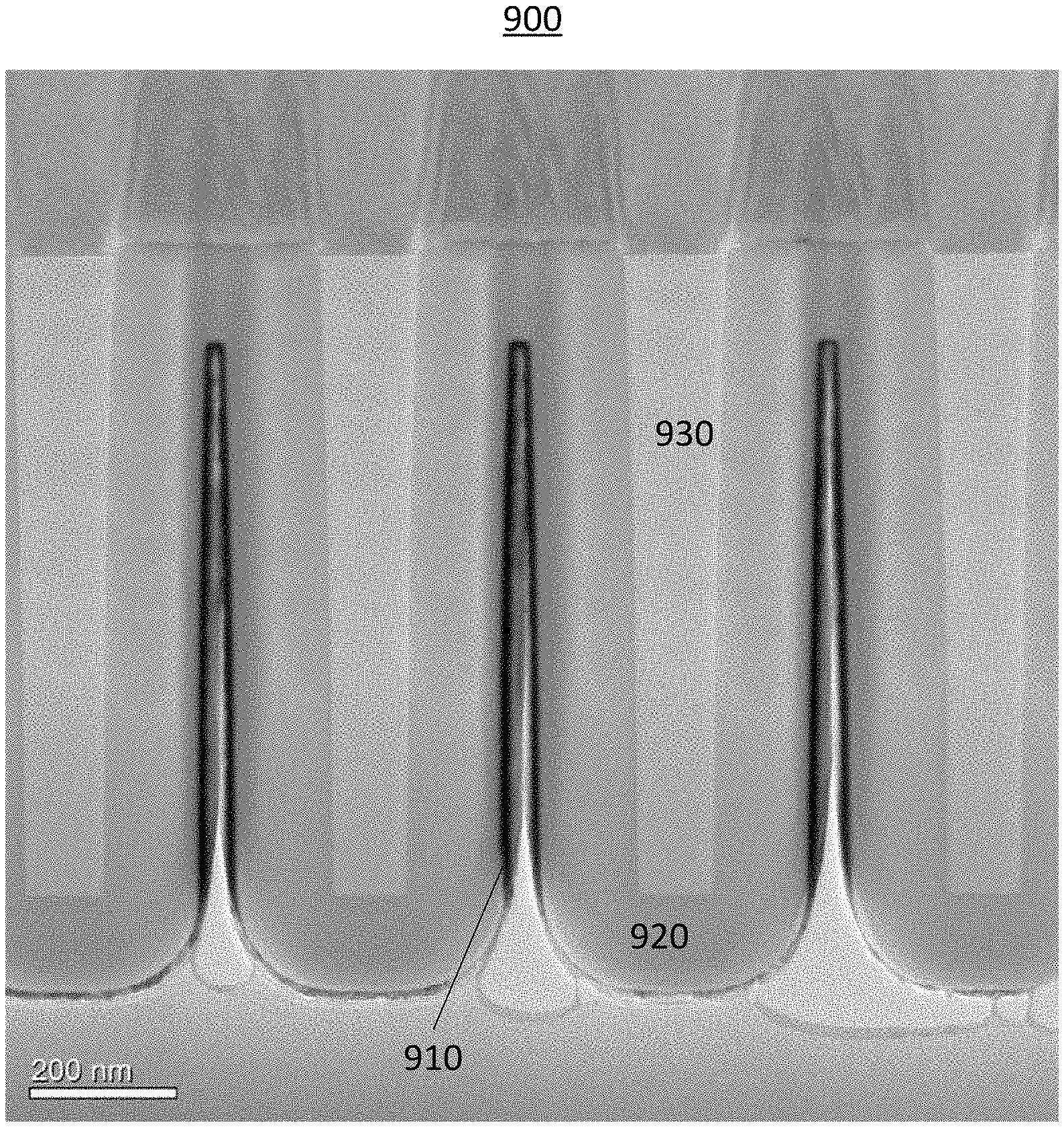
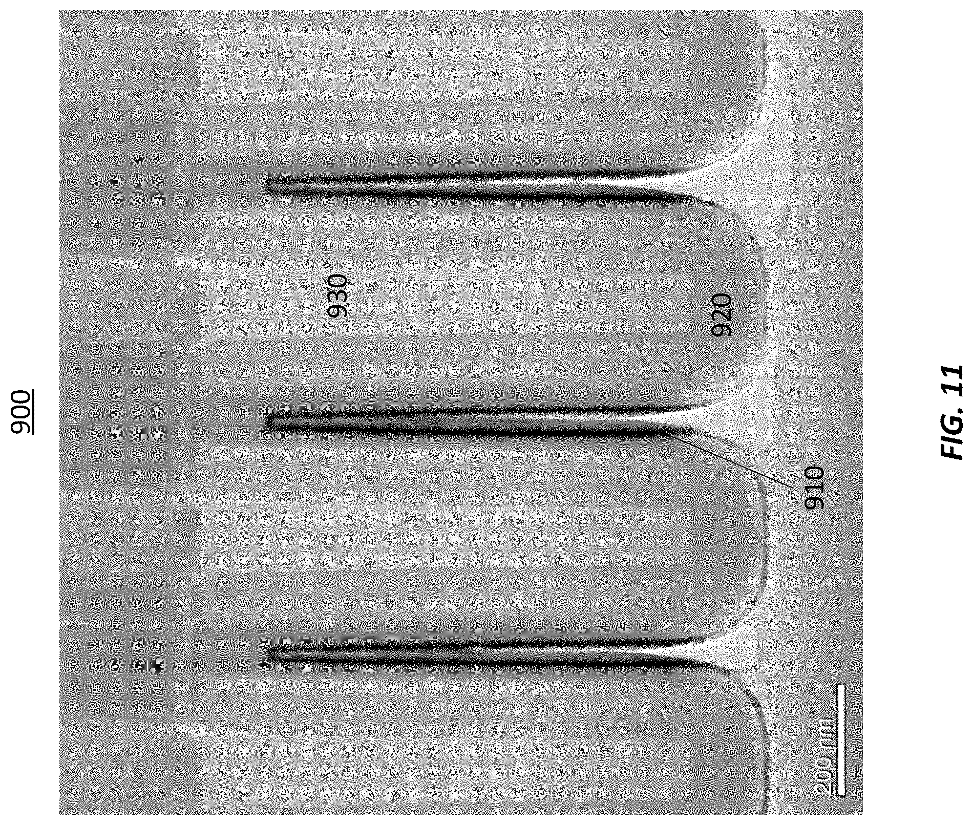
[0064] FIG. 11 illustrates a semiconductor device 900 formed in accordance with at least one embodiment of the invention. The semiconductor device 900 demonstrates good conformality as a result of the hot wire tungsten process on a three dimensional structure having an aspect ratio of 40 (feature depth:width). The tungsten film is conformal on the three-dimensional structure.
[0065] In the preparation of the samples shown in FIG. 11, an aluminum oxide layer was formed on the structures and followed by 0.5 nm amorphous silicon seed layer. A 12 nm deposition of W using hot wire deposition methods described herein followed. Then the samples were capped with thicker layer of amorphous silicon. In some embodiments, the hot-wire deposited metal film (such as selective or non-selective metal film, for example tungsten film) have a step coverage greater than about 50%, greater than about 80%, greater than about 90%, greater than about 95%, greater than about 98%, greater than about 99% or greater in aspect ratios (depth:width) of more than about 2, more than about 5, more than about 10, more than about 20 and in some instances even more than about 40 or more than about 80. It may be noted that aspect ratio may be difficult to determine for the more complicated structures than trenches or vias, but in this context aspect ratio could be understood to be also the ratio of the total surface area of the structures in the wafer/substrate or part of the wafer/substrate in relation to the planar surface area of wafer/substrate or part of the wafer/substrate.
EXAMPLES
[0066] The Examples set forth below are illustrative of various aspects of exemplary embodiments of the present disclosure. The compositions, methods and various parameters reflected therein are intended only to exemplify various aspects and embodiments of the disclosure, and are not intended to limit the scope of the claimed invention.
[0067] 1. A method of forming a metal film comprising: [0068] providing a substrate for processing in a reaction chamber and a hot wire for passing at least a gas through to the reaction chamber, wherein the substrate surface comprises cobalt; [0069] flowing a hydrogen precursor onto the substrate, wherein the hydrogen precursor is contacted with the hot wire; [0070] flowing a metal precursor onto the substrate; and [0071] selectively forming a metal or metallic film on the surface comprising cobalt with a reaction between the metal precursor and the hydrogen precursor contacted with the hot wire.
[0072] 2. The method of example 1, wherein the metal precursor comprises at least one of: a transition metal element; a Group IV element; a Group V element; a Group VI element; Tungsten-containing precursor; a transition metal halide; a transition metal fluoride; tungsten hexafluoride (WF.sub.6); or a Molybdenum-containing precursor, such as molybdenum fluoride, like MoF.sub.5 or MoF.sub.6.
[0073] 3. The method of any of examples 1-2, wherein the hydrogen precursor comprises at least one of: hydrogen (H.sub.2).
[0074] 4. The method of any of examples 1-3, wherein the surface comprises cobalt oxide and flowing a hydrogen precursor over the substrate partially reduces cobalt oxide.
[0075] 5. The method of example 4, wherein the hydrogen precursor contacts the hot wire.
[0076] 6. The method of any of examples 1-5, wherein the metal film formed comprises tungsten.
[0077] 7. The method of any of examples 1-6, wherein selectively forming the metal film comprises an ALD process.
[0078] 8. The method of any of examples 1-7, wherein selectively forming the metal film comprises a cyclic process.
[0079] 9. The method of any of examples 1-8, wherein selectively forming the metal film comprises cyclic or sequential CVD process.
[0080] 10. A reaction chamber, configured to perform the method of any of examples 1-9.
[0081] 11. The method of any of examples 1-10, wherein the substrate surface comprises cobalt oxide.
[0082] 12. The method of example 11, wherein the cobalt oxide is at least reduced partially reduced to metallic cobalt.
[0083] 13. The method of any of examples 1-12, wherein the substrate also comprises another surface comprising SiO.sub.2.
[0084] 14. The method of example 13, wherein the metal or metallic film is selectively deposited on the surface comprising cobalt in relative to another substrate comprising SiO.sub.2.
[0085] 15. The method of any of examples 1-14, wherein the reaction chamber is a hot-wall reaction chamber.
[0086] 16. A method of forming a metal film comprising: [0087] providing a substrate for processing in a reaction chamber and a hot wire for passing at least a gas through to the reaction chamber, wherein the substrate surface comprises cobalt; [0088] exposing the substrate to hydrogen precursor which is contacted with the hot wire; [0089] exposing the substrate to a metal precursor; and [0090] selectively forming a metal or metallic film on the surface comprising cobalt with a reaction between the metal precursor and the hydrogen precursor contacted with the hot wire.
[0091] 17. The method of example 16, wherein the metal precursor comprises at least one of: a transition metal element; a Group IV element; a Group V element; a Group VI element; Tungsten-containing precursor; a transition metal halide; a transition metal fluoride; tungsten hexafluoride (WF.sub.6); or a Molybdenum-containing precursor, such as molybdenum fluoride, like MoF.sub.5 or MoF.sub.6.
[0092] 18. The method of any of examples 16-17, wherein the hydrogen precursor comprises at least one of: hydrogen (H.sub.2).
[0093] 19. The method of any of examples 16-18, wherein the surface comprises cobalt oxide and flowing a hydrogen precursor over the substrate partially reduces cobalt oxide.
[0094] 20. The method of example 19, wherein the hydrogen precursor contacts the hot wire.
[0095] 21. The method of any of examples 16-20, wherein the metal film formed comprises tungsten.
[0096] 22. The method of any of examples 16-21, wherein selectively forming the metal film comprises an ALD process.
[0097] 23. The method of any of examples 16-22, wherein selectively forming the metal film comprises a cyclic process.
[0098] 24. The method of any of examples 16-23, wherein selectively forming the metal film comprises cyclic or sequential CVD process.
[0099] 25. A reaction chamber, configured to perform the method of any of examples 16-24.
[0100] 26. The method of example 16, wherein the substrate surface comprises cobalt oxide.
[0101] 27. The method of example 26, wherein the cobalt oxide is at least reduced partially reduced to metallic cobalt.
[0102] 28. The method of any of examples 16-27, wherein the substrate also comprises another surface comprising SiO.sub.2.
[0103] 29. The method of any of examples 16-28, wherein the metal or metallic film is selectively deposited on the surface comprising cobalt in relative to another substrate comprising SiO.sub.2.
[0104] 30. The method of any of examples 16-29, wherein the reaction chamber is a hot-wall reaction chamber.
[0105] 31. A method of forming a metal film comprising: [0106] providing a substrate having a three-dimensional structure for processing in a reaction chamber and a hot wire for passing at least a gas through to the reaction chamber; [0107] flowing a hydrogen precursor onto the substrate, wherein the hydrogen precursor is contacted with the hot wire; [0108] flowing a metal precursor onto the substrate; and [0109] forming a metal or metallic film on the three-dimensional structure with a reaction between the metal precursor and the hydrogen precursor contacted with the hot wire; and [0110] wherein a metal or metallic film has a step coverage of more than about 50% in three-dimensional structure having aspect ratio of more than about 5.
[0111] 32. The method of example 31, wherein the metal or metallic film has a step coverage of more than about 80% in three-dimensional structure having aspect ratio of more than about 5.
[0112] 33. The method of any of examples 31-32, wherein the metal or metallic film has a step coverage of more than about 50% in three-dimensional structure having aspect ratio of more than about 20.
[0113] 34. The method of any of examples 31-33, wherein the metal or metallic film comprises transition metal film.
[0114] 35. The method of any of examples 31-34, wherein the metal or metallic film is tungsten film.
[0115] 36. The method of any of examples 31-36, wherein reaction chamber is a part of an hot-wall reaction chamber.
[0116] 37. A reaction chamber, configured to perform the method of any of examples 31-36.
[0117] 38. A method of selectively forming a tungsten film comprising: [0118] providing a substrate comprising a first surface and a second surface for processing in a reaction chamber and a hot wire for creating an excited species of a gas; [0119] performing a tungsten precursor pulse/purge step onto the substrate, comprising: [0120] pulsing a tungsten precursor onto the substrate; and [0121] purging an excess of the tungsten precursor from the reaction chamber; and [0122] performing a hydrogen precursor pulse/purge step onto the substrate, comprising: [0123] pulsing a hydrogen precursor onto the substrate, wherein the hydrogen precursor is excited by the hot wire; and [0124] purging an excess of the hydrogen precursor from the reaction chamber; [0125] wherein the tungsten precursor comprises at least one of: tungsten hexafluoride (WF.sub.6); [0126] wherein the hydrogen precursor comprises at least one of: hydrogen (H.sub.2); [0127] wherein a temperature of the hot wire is above about 1000.degree. C.; and [0128] wherein a tungsten film is selectively formed on the first surface.
[0129] 39. The method of example 38, wherein a wall in the reaction chamber is a hot wall.
[0130] 40. The method of example 39, wherein a temperature difference of the hot wall and the substrate may be 100.degree. C., may be less than about 50.degree. C., may be less than about 25.degree. C., may be less than about 5.degree. C., or may be about 0.degree. C.
[0131] 41. The method of example 38, wherein a wall in the reaction chamber is a cold wall.
[0132] 42. The method of example 41, wherein a temperature difference of the cold wall and the substrate may be less than about 100.degree. C., may be less than about 50.degree. C., may be less than about 25.degree. C., may be less than about 5.degree. C., or may be about 0.degree. C.
[0133] 43. The method of any of examples 38-42, wherein a pressure of the reaction chamber ranges between 0.001 mbar and about 1000 mbar, between 0.01 about mbar and about 100 mbar, or between about 0.05 mbar and 20 mbar.
[0134] 44. The method of any of examples 38-43, wherein purging the excess of the tungsten precursor comprises purging the reaction chamber with at least one of: nitrogen (N.sub.2), argon (Ar), helium (He), or other rare or inert gases.
[0135] 45. The method of any of examples 38-42, wherein purging the excess of the hydrogen precursor comprises purging the reaction chamber with at least one of: nitrogen (N.sub.2), argon (Ar), helium (He), or other rare or inert gases.
[0136] 46. A method of selectively forming a film comprising metal, the method comprising: [0137] providing a substrate for processing in a reaction chamber and a hot wire element for contacting at least a gas; [0138] exposing the substrate to a metal precursor; and [0139] exposing the substrate to a gas which has been exposed to a vicinity of the hot wire; [0140] wherein the substrate comprises at least two different materials and the metal film is selectively formed in one of the surfaces.
[0141] 47. The method of example 46, wherein the metal precursor comprises transition metal element.
[0142] 48. The method of example 46, wherein the metal precursor comprises a Group IV, V, or VI element.
[0143] 49. The method of example 46, wherein the metal precursor comprises a tungsten-containing precursor or a molybdenum-containing precursor.
[0144] 50. The method of any of examples 46-49, wherein the gas comprises a reducing gas.
[0145] 51. The method any of examples 46-50, wherein the gas comprises hydrogen.
[0146] 52. The method of example 46, wherein the selectively formed film comprises transition metal.
[0147] 53. The method any of examples 46-52, wherein the selectively formed film comprises metallic material.
[0148] 54. The method any of examples 46-53, wherein the selectively formed film comprises elemental transition metal film.
[0149] 55. The method any of examples 46-54, wherein the selectively formed film comprises elemental tungsten or elemental molybdenum.
[0150] 56. The method of any of examples 46-55, wherein excited radical or atomic species are formed from the gas when the gas has been exposed to a vicinity of the hot wire.
[0151] 57. The method any of examples 46-56, wherein excited radical or atomic species comprising hydrogen are formed from the gas when the gas has been exposed to a vicinity of the hot wire.
[0152] 58. The method any of examples 46-57, wherein the substrate comprises a first surface and a second surface.
[0153] 59. The method of example 58, wherein the first surface comprises a transition metal.
[0154] 60. The method of any of examples 58-59, wherein the first surface comprises an oxidized metal, and underneath the oxidized metal is an elemental metal or metallic conductive film.
[0155] 61. The method of example 58, wherein the second surface comprises silicon.
[0156] 62. The method of example 58, wherein the second surface comprises silicon and oxygen.
[0157] 63. The method of example 62, wherein the second surface comprises Si--O bonds.
[0158] 64. The method of example 58, wherein the second surface comprises SiO.sub.2.
[0159] 65. The method of example 58, wherein the second surface comprises a low-k material.
[0160] 66. The method of example 58, wherein the second surface comprise silicon oxide, silicon nitride, silicon carbide, silicon oxynitride, silicon dioxide, or mixtures thereof
[0161] 67. The method of example 58, wherein the first surface comprises a metal and the second surface comprises silicon and oxygen.
[0162] 68. The method of example 58, wherein the first surface comprises an elemental metal and the second surface comprises silicon and oxygen.
[0163] 69. The method of example 58, wherein first surface comprises a metallic surface and the second surface comprises silicon and oxygen.
[0164] 70. The method of example 58, wherein the first surface comprises W, Cu or Co and the second surface comprises silicon and oxygen.
[0165] 71. The method of any of examples 58-70, wherein the film is selectively formed on the first surface.
[0166] 72. The method any of examples 46-71, further comprising the step of exposing the substrate to a purge gas after the steps of exposing the substrate to the metal precursor.
[0167] 73. The method any of examples 46-72, further comprising the step of exposing the substrate to a purge gas after the steps of exposing the substrate to the gas which has passed through hot wire.
[0168] 74. The method of any of examples 46-73, wherein the hot wire temperature is above 500.degree. C.
[0169] 75. The method of any of examples 46-74, wherein the hot wire temperature is above 1000.degree. C.
[0170] 76. The method of any of examples 46-75, wherein the hot wire temperature is above 1500.degree. C.
[0171] 77. The method of any of examples 46-76, wherein a selectivity is above 50%.
[0172] 78. The method of any of examples 46-77, wherein a selectivity is above 90%.
[0173] 79. The method of example 46, wherein a temperature of the reaction chamber is kept from about 0 to about 800.degree. C.
[0174] 80. The method of any of examples 46-79, wherein the thickness of the film as above 1 nm.
[0175] 81. The method of any of examples 46-80, wherein the thickness of the film as above 5 nm.
[0176] 82. The method of any of examples 46-81, wherein the thickness of the film as above 10 nm.
[0177] 83. The method of any of examples 46-82, wherein the thickness of the film as above 25 nm.
[0178] 84. The method of example 46, wherein a wall in the reaction chamber is a hot wall.
[0179] 85. The method of example 84, wherein a temperature difference of the hot wall and the substrate may be 100.degree. C., may be less than about 50.degree. C., may be less than about 25.degree. C., may be less than about 5.degree. C., or may be about 0.degree. C.
[0180] 86. The method of example 46, wherein a wall in the reaction chamber is a cold wall.
[0181] 87. The method of example 86, wherein a temperature difference of the cold wall and the substrate may be less than about 100.degree. C., may be less than about 50.degree. C., may be less than about 25.degree. C., may be less than about 5.degree. C., or may be about 0.degree. C.
[0182] 88. The method of any of examples 46-87, wherein a pressure of the reaction chamber ranges between 0.001 mbar and about 1000 mbar, between 0.01 about mbar and about 100 mbar, or between about 0.05 mbar and 20 mbar.
[0183] 89. The method of any of examples 46-88, wherein purging the excess of the tungsten precursor comprises purging the reaction chamber with at least one of: nitrogen (N.sub.2), argon (Ar), helium (He), or other rare gases.
[0184] 90. The method of any of examples 46-89, wherein purging the excess of the hydrogen precursor comprises purging the reaction chamber with at least one of: nitrogen (N.sub.2), argon (Ar), helium (He), or other rare gases.
[0185] 91. The method of any of examples 46-90, wherein selectively forming the film comprises an
[0186] ALD process.
[0187] 92. The method of any of examples 46-91, wherein selectively forming the film comprises a cyclic process.
[0188] 93. The method of any of examples 46-92, wherein selectively forming the film comprises cyclic or sequential CVD process.
[0189] 94. A reaction chamber, configured to perform the method of any of examples 46-93.
[0190] 95. A method of forming a tungsten film comprising: [0191] providing a substrate for processing in a reaction chamber and a hot wire for passing at least a gas through to the reaction chamber; [0192] flowing a tungsten precursor onto the substrate; and [0193] flowing a hydrogen precursor onto the substrate, wherein the hydrogen precursor is contacted with the hot wire; and [0194] wherein a reaction between the tungsten precursor and the hydrogen precursor contacted with the hot wire forms a tungsten film; and wherein the reaction chamber is a hot-wall reaction chamber.
[0195] 96. The method of example 95, wherein the tungsten precursor comprises at least one of: tungsten hexafluoride (WF.sub.6).
[0196] 97. The method of any of examples 95-96, wherein the hydrogen precursor comprises at least one of: hydrogen (H.sub.2).
[0197] 98. The method of any of examples 95-97, wherein a temperature of the hot wire ranges about 1000.degree. C., between about 1000 and about 2500.degree. C., between about 1100 and about 2000.degree. C., between about 1200 and about 1900.degree. C., or between 1700 and 1750.degree. C.
[0198] 99. The method of any of example 95-98, further comprising: purging an excess of the tungsten precursor from the reaction chamber.
[0199] 100. The method of any of example 95-99, further comprising: purging an excess of the hydrogen precursor from the reaction chamber.
[0200] 101. The method of any of example 95-100, wherein the formed tungsten film has resistivity of less than about 100 .mu..OMEGA.cm.
[0201] 102. The method of any of example 95-101, wherein the formed tungsten film has resistivity of less than about 50 .mu..OMEGA.cm.
[0202] 103. The method of any of example 95-102, wherein the formed tungsten film has resistivity of less than about 15 .mu..OMEGA.cm.
[0203] 104. The method of any of example 95-103, wherein forming the tungsten film comprises an ALD process.
[0204] 105. The method of any of example 95-104, wherein forming the tungsten the film comprises a cyclic process.
[0205] 106. The method of any of example 95-105, wherein forming the tungsten the film comprises cyclic or sequential CVD process.
[0206] 107. A reaction chamber, configured to perform the method of any of example 95-106.
[0207] The particular implementations shown and described are illustrative of the invention and its best mode and are not intended to otherwise limit the scope of the aspects and implementations in any way. Indeed, for the sake of brevity, conventional manufacturing, connection, preparation, and other functional aspects of the system may not be described in detail. Furthermore, the connecting lines shown in the various figures are intended to represent exemplary functional relationships and/or physical couplings between the various elements. Many alternative or additional functional relationship or physical connections may be present in the practical system, and/or may be absent in some embodiments.
[0208] It is to be understood that the configurations and/or approaches described herein are exemplary in nature, and that these specific embodiments or examples are not to be considered in a limiting sense, because numerous variations are possible. The specific routines or methods described herein may represent one or more of any number of processing strategies. Thus, the various acts illustrated may be performed in the sequence illustrated, in other sequences, or omitted in some cases.
[0209] The subject matter of the present disclosure includes all novel and nonobvious combinations and subcombinations of the various processes, systems, and configurations, and other features, functions, acts, and/or properties disclosed herein, as well as any and all equivalents thereof.
* * * * *
D00000
D00001
D00002
D00003
D00004
D00005
D00006
D00007
D00008
D00009
D00010
D00011
D00012
XML
uspto.report is an independent third-party trademark research tool that is not affiliated, endorsed, or sponsored by the United States Patent and Trademark Office (USPTO) or any other governmental organization. The information provided by uspto.report is based on publicly available data at the time of writing and is intended for informational purposes only.
While we strive to provide accurate and up-to-date information, we do not guarantee the accuracy, completeness, reliability, or suitability of the information displayed on this site. The use of this site is at your own risk. Any reliance you place on such information is therefore strictly at your own risk.
All official trademark data, including owner information, should be verified by visiting the official USPTO website at www.uspto.gov. This site is not intended to replace professional legal advice and should not be used as a substitute for consulting with a legal professional who is knowledgeable about trademark law.