Thin Film Transistor Liquid Crystal Display (tft-lcd) And The Driving Circuit And Switching Power Supply Thereof
LI; Yuntao
U.S. patent application number 16/083391 was filed with the patent office on 2020-10-29 for thin film transistor liquid crystal display (tft-lcd) and the driving circuit and switching power supply thereof. This patent application is currently assigned to Shenzhen China Star Optoelectronics Technology Co., Ltd.. The applicant listed for this patent is SHENZHEN CHINA STAR OPTOELECTRONUCS TECHNOLOGY CO., LTD.. Invention is credited to Yuntao LI.
| Application Number | 20200341310 16/083391 |
| Document ID | / |
| Family ID | 1000004990837 |
| Filed Date | 2020-10-29 |

| United States Patent Application | 20200341310 |
| Kind Code | A1 |
| LI; Yuntao | October 29, 2020 |
THIN FILM TRANSISTOR LIQUID CRYSTAL DISPLAY (TFT-LCD) AND THE DRIVING CIRCUIT AND SWITCHING POWER SUPPLY THEREOF
Abstract
The present disclosure relates to a TFT-LCD and the driving circuit and the switching power supply thereof. The switching power supply includes a PWM controller, an electronic signal generator, and a field effect transistor. The output pins of the electronic signal generator being configured to output voltage signals that vary periodically between multiple voltage ranges. The frequency selection pins of the PWM controller and the output pins of the electronic signal generator are connected to receive the voltage signals from the electronic signal generator, and the PWM controller outputs switching signals of a predetermined frequency through at least one output pin according to a voltage range of the voltage signals received by the frequency selection pins. A gate pin of the FET connects to output pins of the PWM controller, and a source pin of the FET is grounded.
| Inventors: | LI; Yuntao; (Shenzhen, CN) | ||||||||||
| Applicant: |
|
||||||||||
|---|---|---|---|---|---|---|---|---|---|---|---|
| Assignee: | Shenzhen China Star Optoelectronics
Technology Co., Ltd. Shenzhen, Guangdong CN |
||||||||||
| Family ID: | 1000004990837 | ||||||||||
| Appl. No.: | 16/083391 | ||||||||||
| Filed: | July 6, 2018 | ||||||||||
| PCT Filed: | July 6, 2018 | ||||||||||
| PCT NO: | PCT/CN2018/094775 | ||||||||||
| 371 Date: | September 7, 2018 |
| Current U.S. Class: | 1/1 |
| Current CPC Class: | G09G 3/3648 20130101; G02F 1/1368 20130101; G09G 2310/08 20130101; G09G 2330/021 20130101; G02F 1/13306 20130101; H02M 3/156 20130101 |
| International Class: | G02F 1/133 20060101 G02F001/133; G02F 1/1368 20060101 G02F001/1368; H02M 3/156 20060101 H02M003/156; G09G 3/36 20060101 G09G003/36 |
Foreign Application Data
| Date | Code | Application Number |
|---|---|---|
| May 18, 2018 | CN | 201810481375.2 |
Claims
1. A switching power supply, comprising: a pulse width modulation (PWM) controller, an electronic signal generator, and a field effect transistor (FET); wherein output pins of the electronic signal generator being configured to output voltage signals that vary periodically between multiple voltage ranges; wherein frequency selection pins of the PWM controller and the output pins of the electronic signal generator are connected to receive the voltage signals from the electronic signal generator, and the PWM controller outputs switching signals of a predetermined frequency through at least one output pin according to a voltage range of the voltage signals received by the frequency selection pins; and wherein a gate pin of the FET connects to output pins of the PWM controller, and a source pin of the FET is grounded.
2. The switching power supply as claimed in claim 1, wherein the voltage signals are square wave signals.
3. The switching power supply as claimed in claim 2, wherein the voltage signals are clock signals.
4. The switching power supply as claimed in claim 1, wherein the switching power supply further comprises an inductor being connected in series between an input power source of the switching power supply and a drain pin of the FET.
5. The switching power supply as claimed in claim 1, wherein the switching power supply further comprises a crystal triode, a collector pin and an emitter pin of the crystal triode are connected to a drain pin of the FET, and a base pin of the crystal triode is connected to the output pin of the switching power supply.
6. The switching power supply as claimed in claim 5, wherein the crystal triode is a PNP type crystal triode.
7. The switching power supply as claimed in claim 1, wherein the voltage ranges comprises a first voltage range and a second voltage range.
8. The switching power supply as claimed in claim 7, wherein the first voltage range is 0 to 0.7V and the second voltage range is 2.7V to 3.3V; and/or the predetermined frequency corresponding to the first voltage range is 500 kHz, and the predetermined frequency corresponding to the second voltage range is 750 kHz.
9. A driving circuit of TFT-LCD, comprising: a switching power supply comprising a pulse width modulation (PWM) controller, an electronic signal generator, and a field effect transistor (FET); wherein output pins of the electronic signal generator being configured to output voltage signals that vary periodically between multiple voltage ranges; wherein frequency selection pins of the PWM controller and the output pins of the electronic signal generator are connected to receive the voltage signals from the electronic signal generator, and the PWM controller outputs switching signals of a predetermined frequency through at least one output pin according to a voltage range of the voltage signals received by the frequency selection pins; and wherein a gate pin of the FET connects to output pins of the PWM controller, and a source pin of the FET is grounded.
10. The driving circuit as claimed in claim 9, wherein the voltage signals are square wave signals.
11. The driving circuit as claimed in claim 10, wherein the voltage signals are square wave signals.
12. The driving circuit as claimed in claim 9, wherein the switching power supply further comprises an inductor being connected in series between an input power source of the switching power supply and a drain pin of the FET.
13. The driving circuit as claimed in claim 9, wherein the switching power supply further comprises a crystal triode, a collector pin and an emitter pin of the crystal triode are connected to a drain pin of the FET, and a base pin of the crystal triode is connected to the output pin of the switching power supply.
14. The driving circuit as claimed in claim 13, wherein the crystal triode is a PNP type crystal triode.
15. The driving circuit as claimed in claim 9, wherein the voltage ranges comprises a first voltage range and a second voltage range.
16. The driving circuit as claimed in claim 15, wherein the first voltage range is 0 to 0.7V and the second voltage range is 2.7V to 3.3V; and/or the predetermined frequency corresponding to the first voltage range is 500 kHz, and the predetermined frequency corresponding to the second voltage range is 750 kHz.
17. A TFT-LCD comprises the driving circuit as claimed in claim 9.
Description
BACKGROUND
1. Technical Field
[0001] The present disclosure relates to power circuit field, and more particularly to a TFT-LCD and the driving circuit and the switching power supply thereof.
2. Description of Related Art
[0002] A direct circuit (DC)/DC converter circuit of a thin film transistor liquid crystal display (TFT-LCD) mostly uses a switching power supply. The switching power supply converts a higher DC voltage (such as 12V) into a lower DC voltage (such as 5V, 3.3V, 2.5V, etc.) for use in circuits such as microprocessors and image digital processors in the display.
[0003] After the circuit design is completed, the switching frequency of the switching power supply is maintained at a fixed frequency, and the switches in the entire DC/DC circuit will use the same switching frequency. Such a design is easy to make electromagnetic Interference (EMI) radiation at a single frequency to be larger. Due to the lower switching frequency, when the isolation of the power board of the whole machine is not well done, it will cause conduction problems.
SUMMARY
[0004] The present disclosure relates to a TFT-LCD, and the driving circuit and the switching power supply thereof to solve the greater EMI radiation issue and the conduction issues in the TFT-LCD circuit.
[0005] In one aspect, a switching power supply includes: a pulse width modulation (PWM) controller, an electronic signal generator, and a field effect transistor (FET); wherein output pins of the electronic signal generator being configured to output voltage signals that vary periodically between multiple voltage ranges; wherein frequency selection pins of the PWM controller and the output pins of the electronic signal generator are connected to receive the voltage signals from the electronic signal generator, and the PWM controller outputs switching signals of a predetermined frequency through at least one output pin according to a voltage range of the voltage signals received by the frequency selection pins; and wherein a gate pin of the FET connects to output pins of the PWM controller, and a source pin of the FET is grounded.
[0006] Wherein the voltage signals are square wave signals.
[0007] Wherein the voltage signals are clock signals.
[0008] Wherein the switching power supply further includes an inductor being connected in series between an input power source of the switching power supply and a drain pin of the FET.
[0009] Wherein the switching power supply further includes a crystal triode, a collector pin and an emitter pin of the crystal triode are connected to a drain pin of the FET, and a base pin of the crystal triode is connected to the output pin of the switching power supply.
[0010] Wherein the crystal triode is a PNP type crystal triode.
[0011] Wherein the voltage ranges includes a first voltage range and a second voltage range.
[0012] Wherein the first voltage range is 0 to 0.7V and the second voltage range is 2.7V to 3.3V; and/or the predetermined frequency corresponding to the first voltage range is 500 kHz, and the predetermined frequency corresponding to the second voltage range is 750 kHz.
[0013] In another aspect, the present disclosure also provides a driving circuit of TFT-LCDs, and the driving circuit includes the above switching power supply.
[0014] In another aspect, the present disclosure also provides a TFT-LCD, and the TFT-CD includes the above driving circuit.
[0015] According to the switching power supply of the present disclosure, electrical signals whose voltage periodically changes are inserted into a frequency pin of the PWM (PWM) controller, so that the frequency of the switching signals output by the PWM controller periodically changes. The switching power supply is prevented from using the switching signals of the same frequency for a long time, so that the EMI radiation of the circuit is reduced, and the conduction influence amount is reduced.
BRIEF DESCRIPTION OF THE DRAWINGS
[0016] In order to more clearly illustrate the embodiments of the present disclosure or prior art solutions, the drawings used in the description of the embodiments or prior art will be briefly described below. The drawings are merely some embodiments of the present disclosure, and those skilled in the art can also obtain other drawings based on these drawings without any creative work.
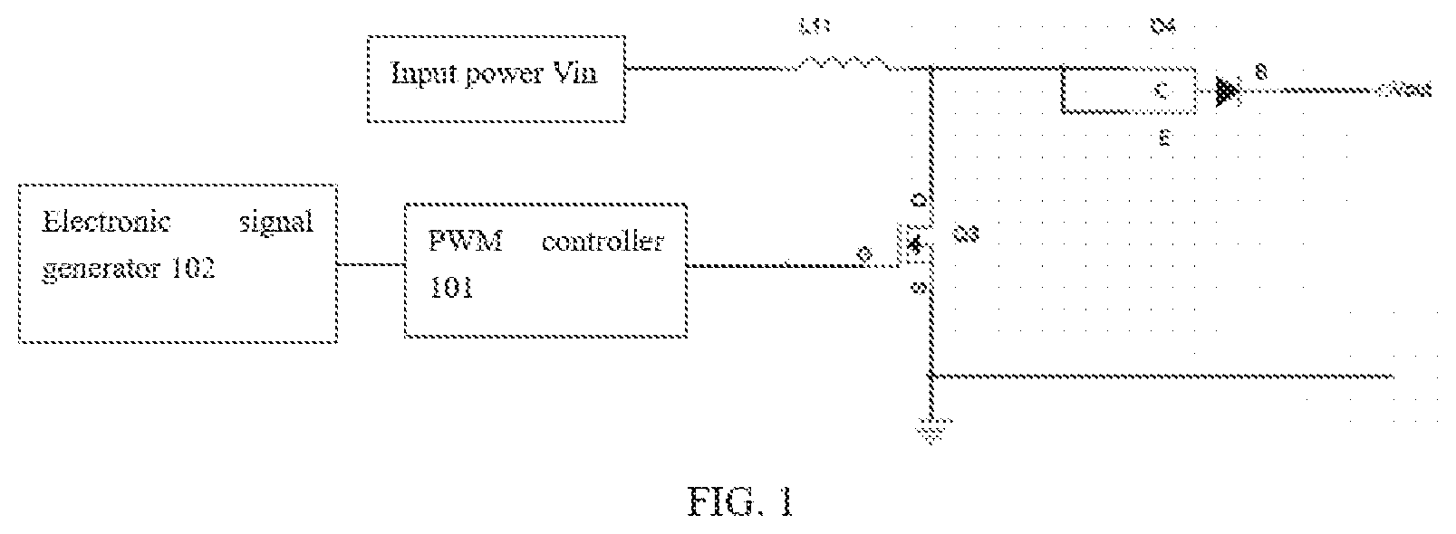
[0017] FIG. 1 is a schematic view of the circuit of the switching power supply in accordance with one embodiment of the present disclosure.
DETAILED DESCRIPTION
[0018] Following embodiments of the invention will now be described in detail hereinafter with reference to the accompanying drawings.
[0019] In the drawings, the thicknesses of layers and regions may be exaggerated for clarity. Same reference numerals refer to the same components throughout the specification and the drawings.
[0020] FIG. 1 is a schematic view of the circuit of the switching power supply in accordance with one embodiment of the present disclosure.
[0021] As shown in FIG. 1, the switching power supply includes a PWM controller 101, an electronic signal generator 102, and a field effect transistor (FET) (Q3).
[0022] The electrical signal generator 102 can be a variety of devices that can generate voltage signals that vary periodically between multiple voltage ranges. The electrical signal generator 102 can be an electrical signal generator specifically provided for the switching power supply, or an electrical signal generator shared by the switching power supply and a circuit using the switching power supply (for example, a TFT-LCD display circuit).
[0023] The electrical signal generator 102 outputs voltage signals that periodically changes between a plurality of voltage ranges through its output pin. In one embodiment, the plurality of voltage ranges are two voltage ranges, a first voltage range and a second voltage range, respectively. The voltage value in the first voltage range is less than the voltage value in the second voltage range. As an example, the first voltage range is 0 to 0.7V and the second voltage range is 2.7V to 3.3V.
[0024] The voltage signals can be square wave signal. For example, the voltage signal can be a clock signal in a square wave signal or other periodically varying signal.
[0025] The PWM controller 101 includes frequency selection pins (FSEL) and output pins.
[0026] The FSEL of the PWM controller 101 and the output pins of the electronic signal generator 102 are connected so as to receive the voltage signal from the electronic signal generator 102. The voltage signal periodically changes between a plurality of voltage ranges through its output pin.
[0027] The PWM controller 101 outputs a switching signal of a predetermined frequency through at least one output pin according to a voltage range of a voltage signal received by the FSEL pin. Specifically, the PWM controller 101 outputs a switching signal of a predetermined frequency corresponding to the voltage range of the voltage signal. Since the voltage signal periodically changes between a plurality of voltage ranges, the frequency of the switching signal output from the PWM controller 101 also periodically changes.
[0028] In an example, the plurality of voltage ranges includes the first voltage range and the second voltage range. When the voltage signal received by the PWM controller 101 through the frequency pin is in the first voltage range, the PWM controller 101 outputs a switching signal of a predetermined frequency corresponding to the first voltage range through the output pin; when the voltage signal received by the PWM controller 101 through the frequency pin is in the second voltage range, the PWM controller 101 outputs the switching signal of a predetermined frequency corresponding to the second voltage range via the output pins.
[0029] As an example, the predetermined frequency corresponding to the first voltage range is 500 kHz, and the predetermined frequency corresponding to the second voltage range is 750 kHz. That is, in the case where the plurality of voltage ranges includes the first voltage range and the second voltage range, the frequency of the switching signal output from the PWM controller 101 periodically jumps between 500 kHz and 750 kHz.
[0030] The gate pin G of the FET Q3 is connected to the output pin of the PWM controller 101, and the source pin S is grounded. Since the gate pin G of the FET Q3 is connected to the output pin of the PWM controller 101, that is, the gate pin G of the FET Q3 receives a switching signal of a predetermined frequency. The switching signal can control whether the conduction between the source pin S and drain D pin is turned on or off.
[0031] In another embodiment, the switching power supply further includes an inductor L11. The inductor L11 is connected in series between an input power source Vin of the switching power supply and the drain pin D of the FET Q3.
[0032] In addition, the switching power supply may further include a crystal triode D4. The collector pin C, the emitter pin of the crystal triode D4 are connected to the drain pin D of the FET Q3, and the base pin B of the crystal triode D4 is connected to the output pin Vout of the switching power supply. The crystal triode can be various types of crystal triodes. For example, the crystal triode is a PNP type crystal triode.
[0033] The present disclosure further provides a driving circuit of a TFT-LCD. The driving circuit includes the above switching power supply.
[0034] The present disclosure further provides a TFT-LCD including the above driving circuit.
[0035] In view of the above, an electrical signal whose voltage periodically changes is inserted at a frequency pin of the PWM controller, so that the frequency of the switching signal output by the PWM controller periodically changes. The switching power supply is prevented from using the switching signal of the same frequency for a long time, so that the EMI radiation of the circuit is reduced, and the conduction influence amount is reduced.
[0036] The above description is merely the embodiments in the present disclosure, the claim is not limited to the description thereby. The equivalent structure or changing of the process of the content of the description and the figures, or to implement to other technical field directly or indirectly should be included in the claim.
* * * * *
D00000
D00001
XML
uspto.report is an independent third-party trademark research tool that is not affiliated, endorsed, or sponsored by the United States Patent and Trademark Office (USPTO) or any other governmental organization. The information provided by uspto.report is based on publicly available data at the time of writing and is intended for informational purposes only.
While we strive to provide accurate and up-to-date information, we do not guarantee the accuracy, completeness, reliability, or suitability of the information displayed on this site. The use of this site is at your own risk. Any reliance you place on such information is therefore strictly at your own risk.
All official trademark data, including owner information, should be verified by visiting the official USPTO website at www.uspto.gov. This site is not intended to replace professional legal advice and should not be used as a substitute for consulting with a legal professional who is knowledgeable about trademark law.