Holographic Waveguide Light Field Displays
Popovich; Milan Momcilo ; et al.
U.S. patent application number 16/820601 was filed with the patent office on 2020-10-29 for holographic waveguide light field displays. This patent application is currently assigned to DigiLens Inc.. The applicant listed for this patent is DigiLens Inc.. Invention is credited to Alastair John Grant, Milan Momcilo Popovich, Jonathan David Waldern.
| Application Number | 20200341272 16/820601 |
| Document ID | / |
| Family ID | 1000004750075 |
| Filed Date | 2020-10-29 |

| United States Patent Application | 20200341272 |
| Kind Code | A1 |
| Popovich; Milan Momcilo ; et al. | October 29, 2020 |
Holographic Waveguide Light Field Displays
Abstract
A light field display, having at least one laser emitter, an optical modulator for modulating light from the laser emitter with video information; a beam focus modulator; an array of beam scanning elements; an electrically controllable beam focus modulator; and at least one at least one waveguide having at least one transparent substrate, an input grating and an output grating for extracting light from the waveguide; and an eye tracker is provided.
| Inventors: | Popovich; Milan Momcilo; (Leicester, GB) ; Waldern; Jonathan David; (Los Altos Hills, CA) ; Grant; Alastair John; (San Jose, CA) | ||||||||||
| Applicant: |
|
||||||||||
|---|---|---|---|---|---|---|---|---|---|---|---|
| Assignee: | DigiLens Inc. Sunnyvale CA |
||||||||||
| Family ID: | 1000004750075 | ||||||||||
| Appl. No.: | 16/820601 | ||||||||||
| Filed: | March 16, 2020 |
Related U.S. Patent Documents
| Application Number | Filing Date | Patent Number | ||
|---|---|---|---|---|
| 15543013 | Jul 12, 2017 | |||
| PCT/GB2016/000003 | Jan 11, 2016 | |||
| 16820601 | ||||
| 62125089 | Jan 12, 2015 | |||
| 62125066 | Jan 12, 2015 | |||
| Current U.S. Class: | 1/1 |
| Current CPC Class: | G02B 27/48 20130101; G02F 1/29 20130101; G02B 6/0035 20130101; G02B 6/0016 20130101; G02B 27/0103 20130101; G02B 2027/0125 20130101; G02B 2027/0187 20130101; G02B 6/0065 20130101; G02B 27/0172 20130101; G02B 27/0093 20130101; G02B 2027/0185 20130101; G02B 6/0076 20130101; G02B 2027/0174 20130101 |
| International Class: | G02B 27/01 20060101 G02B027/01; G02B 27/00 20060101 G02B027/00; F21V 8/00 20060101 F21V008/00; G02B 27/48 20060101 G02B027/48; G02F 1/29 20060101 G02F001/29 |
Claims
1. A light field display, comprising: at least one laser emitter; an optical modulator for modulating light from said laser emitter with video information; at least one eye tracker for determining the gaze direction of a viewer of said display; an electronically controllable beam focus modulator for focusing said video-modulated light onto one or more focal surfaces determined using said eye tracker for presentation to a view of said display; an array of electronically addressable beam scanning elements for projecting said video-modulated light over a field of view wherein each element scans said light around an average direction vector; at least one waveguide, said waveguide comprising at least one transparent substrate, an input grating for coupling said focused video-modulated light into a TIR path and an output grating for extracting light from said waveguide for viewing; at least one holographic diffuser; and a microlens array overlaying said holographic diffuser and disposed between said holographic diffuser and a viewer of said display; wherein: the determination of a gaze direction vector causes the beam scanning element with an average direction vector closest to said gaze direction to be addressed; said addressed beam scanning element sweeps a portion of said image-modulated light to the input grating of the at least one waveguide; and the light extracted from said waveguide is focused onto said holographic diffuser and reimaged by said microlens array to present a light field image to a viewer of said display.
2. The apparatus of claim 1 wherein said array of beam scanning elements includes elements for high resolution foveal image scanning and elements for low resolution peripheral image scanning.
3. The apparatus of claim 1 wherein separate waveguides are provided for red, green and blue image light.
4. The apparatus of claim 1 wherein said eye tracker is a waveguide device.
5. The apparatus of claim 1 wherein elements of said scanner array are one of movable fibers, movable gratings, or micro mirrors.
6. The apparatus of claim 1 wherein said beam focus modulator is one of a lens formed in an adaptive polymer, a lens formed by a liquid crystal layer combined with a diffractive or refractive element, a spatial light modulator or a fluidic lens.
7. The apparatus of claim 1 wherein separate left and right eye trackers are provided.
8. The apparatus of claim 1 incorporating a GRIN waveguide.
9. The apparatus of claim 1 wherein said at least one laser emitter contains at least one red, at least one green and at least one blue die.
10. The apparatus of claim 1 wherein said output grating is configured as a tessellated array of switchable gratings.
11. The apparatus of claim 1 wherein said gratings are one of a Bragg Grating, a surface relief grating or a switchable Bragg grating recorded in a HPDLC material, a uniform modulation HPDLC material or a reverse mode HPDLC material.
12. The apparatus of claim 1 further comprising a waveguide despeckler.
13. A waveguide light field display comprising: an input image generator providing image light projected over a field of view; at least one imaging waveguide, said imaging waveguide comprising an input grating for coupling image light into a TIR path and an output grating for extracting light from said imaging waveguide to form an intermediate image. a diffuser disposed in proximity to said intermediate image; and a lens array having a focal surface disposed in proximity to said diffuse for forming a viewable image.
14. The apparatus of claim 13 wherein separate imaging waveguides are provided for red, green and blue image light.
15. The apparatus of claim 13 wherein a waveguide eye tracker is disposed as a layer on top of said imaging waveguide.
16. The apparatus of claim 13 wherein said image generator comprises a microdisplay and a collimating lens.
17. The apparatus of claim 13 wherein said image generator is a laser scanner.
18. The apparatus of claim 13 wherein said output grating is a two dimensional array of selectively switching grating elements.
19. The apparatus of claim 13 further comprising a waveguide despeckler.
20. The apparatus of claim 13 wherein said output grating is one of a Bragg Grating, a surface relief grating or a switchable Bragg grating recorded in a HPDLC material, a uniform modulation HPDLC material or a reverse mode HPDLC material.
Description
PRIORITY CLAIMS
[0001] This application claims priority from U.S. Provisional Application Ser. No. 62/125,089 entitled HOLOGRAPHIC WAVEGUIDE LIGHT FIELD DISPLAYS filed on 12 Jan. 2015 and U.S. Provisional Application Ser. No. 62/125,066 entitled OPTICAL WAVEGUIDE DISPLAYS FOR INTEGRATION IN WINDOWS filed on 12 Jan. 2015, each of which is hereby incorporated by reference in its entirety.
CROSS REFERENCE TO RELATED APPLICATIONS
[0002] The following patent applications are incorporated by reference herein in their entireties: U.S. Pat. No. 6,115,152 entitled HOLOGRAPHIC ILLUMINATION SYSTEM, U.S. Pat. No. 8,233,204 entitled OPTICAL DISPLAYS, PCT Application No.: US2006/043938, entitled METHOD AND APPARATUS FOR PROVIDING A TRANSPARENT DISPLAY, PCT Application No.: PCT/GB2012/000680, entitled IMPROVEMENTS TO HOLOGRAPHIC POLYMER DISPERSED LIQUID CRYSTAL MATERIALS AND DEVICES, PCT Application No.: GB2012/000677 entitled WEARABLE DATA DISPLAY, U.S. patent application Ser. No. 13/317,468 entitled COMPACT EDGE ILLUMINATED EYEGLASS DISPLAY, U.S. patent application Ser. No. 13/869,866 entitled HOLOGRAPHIC WIDE ANGLE DISPLAY, and U.S. patent application Ser. No. 13/844,456 entitled TRANSPARENT WAVEGUIDE DISPLAY, PCT Application No.: PCT/GB2013/000500 entitled WAVEGUIDE FOR HOMOGENIZING ILLUMINATION, U.S. Pat. No. 8,224,133 entitled LASER ILLUMINATION DEVICE and PCT Application No.: GB2010/001920 entitled COMPACT EDGE ILLUMINATED DIFFRACTIVE DISPLAY.
BACKGROUND OF THE INVENTION
[0003] This invention relates to a display device, and more particularly to a light field display based on holographic waveguides.
[0004] Light field displays convert the phase distribution of a wavefront into angular distribution of light rays allowing the correction perception of a 3D scene. The light field is essentially a set of image surfaces distributed within a viewing volume. The number of surfaces required depends on the application but in some cases can be as few as four. Traditionally light field displays have used arrays of lens to project a phase distribution recorded into a photographic emulsion or spatial light modulator. A more recent approach to light field displays is one disclosed in United States Patent Application No. US2014/0003762 by Macnamara entitled MULTIPLE DEPTH PLANE THREE-DIMENSIONAL DISPLAY USING WAVEGUIDE REFLECTOR ARRAY PROJECTOR.
[0005] There is growing interest in applying light field displays in applications such as virtual reality and augmented reality. A wearable light field display would be an advantage in such applications. However, current designs are bulky and lack the transparency required for applications such as augmented reality. Waveguide displays are the key to provide high optical performance in a compact, transparent display.
[0006] There is a requirement for a compact transparent light field display based on a holographic waveguide.
SUMMARY OF THE INVENTION
[0007] It is a first object of the invention to provide a compact transparent light field display based on a holographic waveguide.
[0008] The objects of the invention are achieved in one embodiment of the invention in which there is provided a light field display, comprising: at least one laser emitter; an optical modulator for modulating light from the laser emitter with video information; an electronically controllable beam focus modulator; an array of electronically addressable beam scanning elements for projecting the image-modulated light over a field of view wherein each element scans the light around an average direction vector; an electrically controllable beam focus modulator; at least one waveguide and at least one eye tracker. The waveguide comprises at least one transparent substrate, an input grating for coupling image light into a TIR path and an output grating for extracting light from the waveguide for viewing. The beam focus modulator focuses the light onto an eye accommodation surface determined using the eye tracker. The beam scanning element addressed at any time is the one with an average direction vector most closely corresponding to the gaze direction determined using the eye tracker.
[0009] In one embodiment the array of beam scanning elements includes elements for high resolution foveal image scanning and elements for low resolution peripheral image scanning.
[0010] In one embodiment separate waveguides are provided for red, green and blue image light.
[0011] In one embodiment the eye tracker is a waveguide device.
[0012] In one embodiment the elements of the scanner array are movable fibers, movable gratings, or micro mirrors.
[0013] In one embodiment the beam focus modulator is a lens formed in an adaptive polymer, a lens formed by a liquid crystal layer combined with a diffractive or refractive element, a spatial light modulator or a fluidic lens.
[0014] In one embodiment separate left and right eye trackers are provided.
[0015] In one embodiment the light field display incorporates a GRIN waveguide.
[0016] In one embodiment the laser array contains at least one red, at least one green and at least one blue die.
[0017] In one embodiment the output grating is configured as a tessellated array of switchable gratings.
[0018] In one embodiment the grating is a holographic grating recorded in a Bragg Grating, a surface relief grating or a switchable Bragg grating recorded in a HPDLC material, a uniform modulation HPDLC material or a reverse mode HPDLC material.
[0019] In one embodiment the light field display further comprises a waveguide despeckler.
[0020] In one embodiment waveguide light field display comprises: an input image generator providing image light projected over a field of view; at least one imaging waveguide, the imaging waveguide comprising an input grating for coupling image light into a TIR path and an output grating for extracting light from the imaging waveguide to form an intermediate image; a diffuser disposed in proximity to the intermediate image; and a lens array having a total surface disposed in proximity to the diffuse layer for forming a viewable image.
[0021] In one embodiment separate imaging waveguides are provided for red, green and blue image light.
[0022] In one embodiment a waveguide eye tracker is disposed as a layer on top of the imaging waveguide.
[0023] In one embodiment the image generator comprises a microdisplay and a collimating lens.
[0024] In one embodiment the image generator is a laser scanner.
[0025] In one embodiment output grating is a two dimensional array of selectively switching grating elements.
[0026] In one embodiment the light field display further comprises a waveguide despeckler.
[0027] In one embodiment at least one of the gratings is a holographic grating recorded in a Bragg Grating, a surface relief grating or a switchable Bragg grating recorded in a HPDLC material, a uniform modulation HPDLC material or a reverse mode HPDLC material.
[0028] A more complete understanding of the invention can be obtained by considering the following detailed description in conjunction with the accompanying drawings, wherein like index numerals indicate like parts. For purposes of clarity, details relating to technical material that is known in the technical fields related to the invention have not been described in detail.
BRIEF DESCRIPTION OF THE DRAWINGS
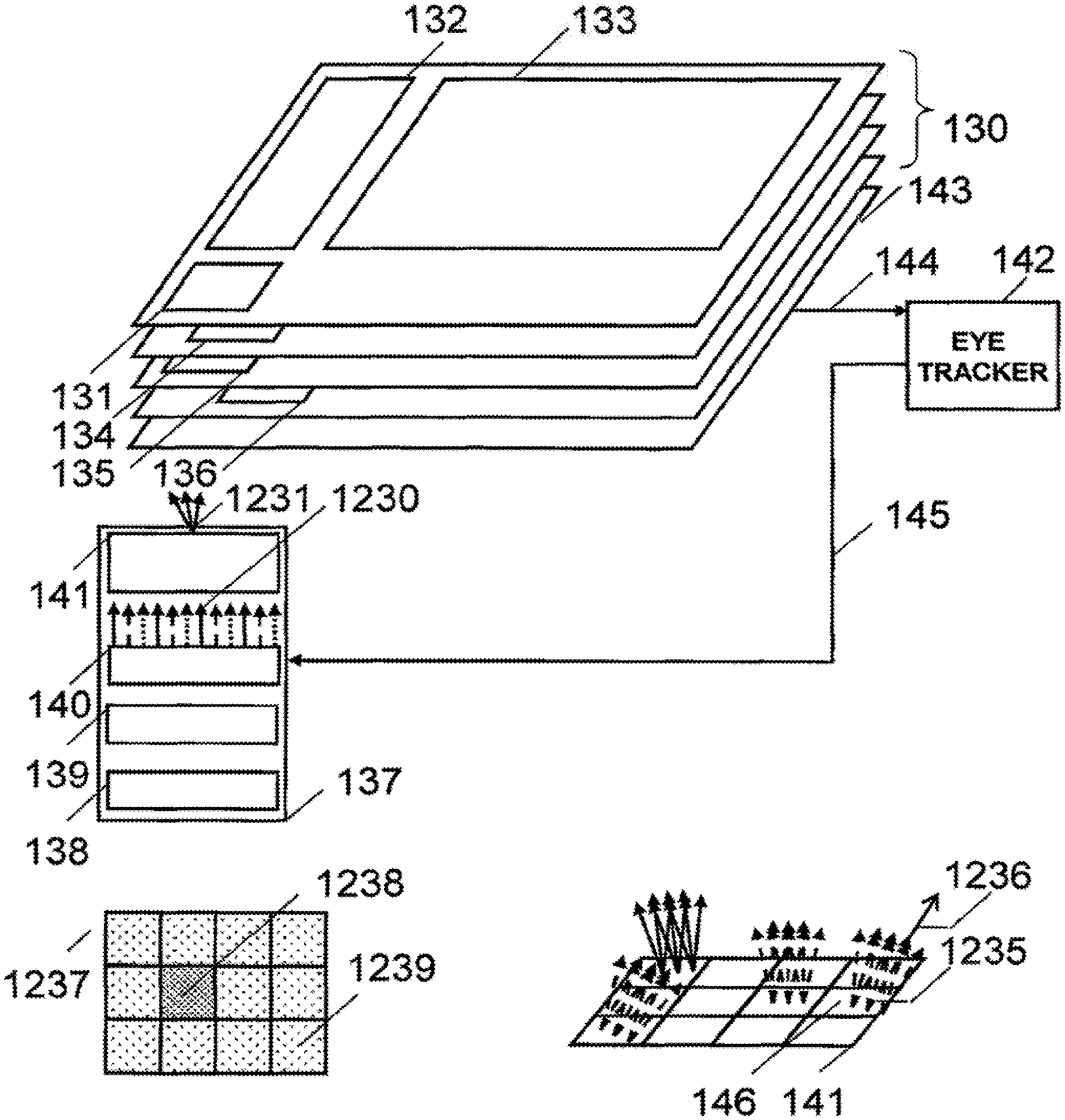
[0029] FIG. 1A is a schematic view of a holographic waveguide light field display in one embodiment.
[0030] FIG. 1B is a schematic view showing the image field formed by holographic waveguide light field display in one embodiment.
[0031] FIG. 1C is a schematic view of a scanner module use in a holographic waveguide light field display in one embodiment.
[0032] FIG. 2A is a cross section view of a monochrome light field display using a holographic lens array in one embodiment.
[0033] FIG. 2B is a cross section view of a detail of a monochrome light field display using a holographic lens array in one embodiment.
[0034] FIG. 2C is a plan view of a detail of a monochrome light field display using a holographic lens array in one embodiment.
[0035] FIG. 2D is a plan view of a microdisplay panel used in a monochrome light field display using a holographic lens array in one embodiment.
[0036] FIG. 2E is a plan view of a detail of a monochrome light field display using a holographic lens array in one embodiment.
[0037] FIG. 3A is a cross section view of a color light field display using a holographic lens array in one embodiment.
[0038] FIG. 3B is a plan view of a detail of color light field display using a holographic lens array in one embodiment.
[0039] FIG. 3C is a cross section view of a detail of a color light field display using a holographic lens array in one embodiment.
[0040] FIG. 3D is a plan view of a microdisplay panel used in a color light field display using a holographic lens array in one embodiment.
[0041] FIG. 3E is a plan view of a detail of a color light field display using a holographic lens array in one embodiment.
[0042] FIG. 4 is a general architecture for a light field display based on GRIN waveguide and diffractive waveguide optics in one embodiment.
[0043] FIG. 5 is a schematic side view of a GRIN waveguide in embodiment of the invention.
[0044] FIG. 6 is a general architecture for a light field display based on GRIN waveguide and diffractive waveguide optics in one embodiment.
[0045] FIG. 7 is a general architecture for a light field display based on GRIN waveguide and diffractive waveguide optics in one embodiment.
DETAILED DESCRIPTION OF THE INVENTION
[0046] The invention will now be further described by way of example only with reference to the accompanying drawings. It will apparent to those skilled in the art that the present invention may be practiced with some or all of the present invention as disclosed in the following description. For the purposes of explaining the invention well-known features of optical technology known to those skilled in the art of optical design and visual displays have been omitted or simplified in order not to obscure the basic principles of the invention. Unless otherwise stated the term "on-axis" in relation to a ray or a beam direction refers to propagation parallel to an axis normal to the surfaces of the optical components described in relation to the invention. In the following description the terms light, ray, beam and direction may be used interchangeably and in association with each other to indicate the direction of propagation of light energy along rectilinear trajectories. Parts of the following description will be presented using terminology commonly employed by those skilled in the art of optical design. It should also be noted that in the following description of the invention repeated usage of the phrase "in one embodiment" does not necessarily refer to the same embodiment.
[0047] A waveguide light field display according to the principles of the invention is shown in FIG. 1. Referring first to FIG. 1A we see that the apparatus comprises a stack of waveguide layer generally indicated by 130, each layer containing an input grating 131 a fold grating 132 and an output grating 133. The input grating has high efficiency for maximum light in-coupling efficiency. In one embodiment output grating is a lossy grating for extracting light uniformly out of the waveguide along the beam path. In contrast to the input and output gratings which deflect light in a plane orthogonal to the waveguide the fold grating deflects light substantially in the plane of the waveguide. Input images are provided by a scanning module 137 comprising the laser array 138 which contains multiple red, green, blue die. The intensities of the beams are modulated with image information by the video modulator 139. A beam focus modulator 140 controls the instantaneous beam divergence or accommodation of each beam. Finally, a scanner array device 141 scans the focus-adjusted beams 1230 providing a multiplicity of ray directions in 3D space as indicated by 1231. Each ray direction corresponds to a unique viewing direction as perceived by a person viewing the display. The scanning module operates under the control of an eye tracker which supplies instantaneous eye gaze direction vector and accommodation state. The eye tracker is waveguide devices represented by the layer 143. The data links from the eye tracker waveguide to the eye tracker processing module 142 and from the eye tracker processing module to the scanning module are indicated by 144,145. Advantageously, the eye tracker is based on one of the embodiments of PCT Application No.: PCT/GB2014/000197 entitled HOLOGRAPHIC WAVEGUIDE EYE TRACKER by Popovich et al. The scanning module may also include a laser despeckler. Advantageously the despeckler is an electro optical device and specifically a waveguide SBG device based on the embodiments of PCT Application No.: PCT/GB2013/000500 entitled WAVEGUIDE FOR HOMOGENIZING ILLUMINATION, and U.S. Pat. No. 8,224,133 entitled LASER ILLUMINATION DEVICE both of which are incorporated herein by reference in their entireties. The gratings in different layers may be staggered or rotated as indicted by the laterally displace input gratings 134-136.
[0048] The gratings may be switching (SBGs) or non-switching. The inventors believe that a passive solution is achievable by controlling the wavelength and beam angle diversity of the scanning input beams we can create Bragg-separated paths through the waveguides, thus minimising the risk of crosstalk and re-coupling. The design variables are the grating K-vectors and the fibre output beam vectors.
[0049] In one embodiment the scanning module further comprises a microlens array in front of the laser module for beam expansion.
[0050] The output image provided by the display is shown in FIG. 1B. The image 1237 which is represented in field of view space comprises tiles including a high resolution tile 1238 corresponding to the detected gaze direction of the viewer's eye and low resolution tiles such as 1239. This type of image rendering scheme is commonly referred to, in computer graphics, as foveated rendering the goal being to reducing image processing latency by concentrating detail in small field of view region corresponding to the human eye's foveal field.
[0051] The scanner array device 141 is shown in more detail in FIG. 1C which represents the output surfaces of the array and shows the output ray directions at different array elements. The scanner array comprises discrete 3D scanning elements such as 146 which sweep collimated (focus adjusted) beams over an angular range around a defined direction vector 1236, each scanner element having a unique direction vector. In one embodiment scanner elements can be switched between high and low resolution scanning correspond to foveal and background resolution in the final image. In one embodiment the scanner resolution can be controlled to provide a larger number of resolutions steps from foveal resolution to a very low background resolution thereby providing a better match to the eye's resolution response curve. In one embodiment each scanner element operates on red, green and blue light sequentially.
[0052] The invention does not assume any specific method for scanning the beam. In one embodiment the scanner array comprises an array of optical fibers having optical axes translated or rotated by one or more mechanical transducers according to the teachings of United States Patent Application No. US2014/0003762 by Macnamara. In one embodiment the scanner array comprises an array of gratings having surface normal translated or rotated by one or more mechanical transducers. In one embodiment the scanner array comprises an array of microlens having their optical axes translated or rotated by one or more mechanical transducers. In one embodiment the scanner array is provided by time-varying diffractive structures written into a spatial light modulator array. In one embodiment the scanner array is provided by a micro electro mechanical mirror array. Other schemes for providing a beam scanning array are to be found in the literature of optical scanners and optical radar systems.
[0053] In one embodiment at least one grating in at least one of the layers is a multiplexed grating operating on more than one wavelength or image field of view range. That is the two or more gratings having prescription covering different wavelength bands or angular bands are combined in holographic layer. Multiplexing offers potential for a significant reduction in the number of waveguide layers required. A key prerequisite for multiplexing is a high refractive index modulation.
[0054] In one embodiment the gratings are recorded in uniform modulation liquid crystal-polymer gratings such as the ones disclosed in United State Patent Application Publication No.: US2007/0019152 by Caputo et al and PCT Application No.: PCT/EP2005/006950 by Stumpe et al. both of which are incorporated herein by reference in their entireties. Uniform modulation gratings are characterized by high refractive index modulation (and hence high diffraction efficiency) and low scatter. The latter is a key factor in reducing the number of waveguide layers.
[0055] The inventors believe that the embodiment of FIG. 1 can provide 100.degree..times.50.degree. field of view light field display using four waveguide layers each providing a pupil expanded 25.degree..times.50.degree. tile. This applies to a monochrome display. If we assume that reasonable colour gamut can be provided by have separate waveguides for red and blue/green the number of layers is increased by .times.2. However, multiplexing (in angular or colour space) decreases the number of layers by .times.2.
[0056] In one embodiment the output gratings are tessellated in the manner disclosed in U.S. patent application Ser. No. 13/869,866 entitled HOLOGRAPHIC WIDE ANGLE DISPLAY
[0057] Accommodation control is a key component of a practical light field display. It can be implemented in several different ways. In one embodiment the beam focus modulator 140 is based on the approach disclosed in US2014/0003762 by Macnamara of using a miniature deformable membrane mirror before it is raster-scanned and projected to the viewer's eyes. However, accommodation control a dynamic research field and there are several other approaches that may be considered for use with the present invention including fluidic lenses, adaptive polymers, liquid crystal lenses, and hybrid LC-diffractive refractive lens systems. Any of these approaches may be used to provide the beam focus modulator 140. Liquid crystal lens accommodation control is based on a mixture of liquid crystal molecules and smaller monomers placed between two glass substrates coated with a layer of conducting indium tin oxide. A concave glass lens is then placed on top of one of the substrates. Without applying any voltage, the liquid-crystals/monomer is uniformly distributed throughout the substrates. After applying a voltage across the two substrates, however, the liquid crystal molecules move to either end of the gap, where the electric field is higher, while the monomers move toward the middle, where the electric field is lower. Thus, the refractive index can be varied across the device allowing it to function as a lens. Exemplary liquid crystal lenses are manufactured by OKO Technologies (Delft, The Netherlands. Fluidic lenses comprise a transparent optical fluid encapsulated within a flexible lens membrane and substrate (top). Upon compression of the lens body, the shape of the flexible lens membrane is modified, which results in an adjustment of the focal length of the lens (bottom). Exemplary electro active polymer lenses have been developed by the University of Central Florida (Orlando, Fla., USA; www.ucf.edu). In one embodiment the beam focus modulator 140 may also be used to provide dynamic aberration correction (if the aberrations can be defined a priori).
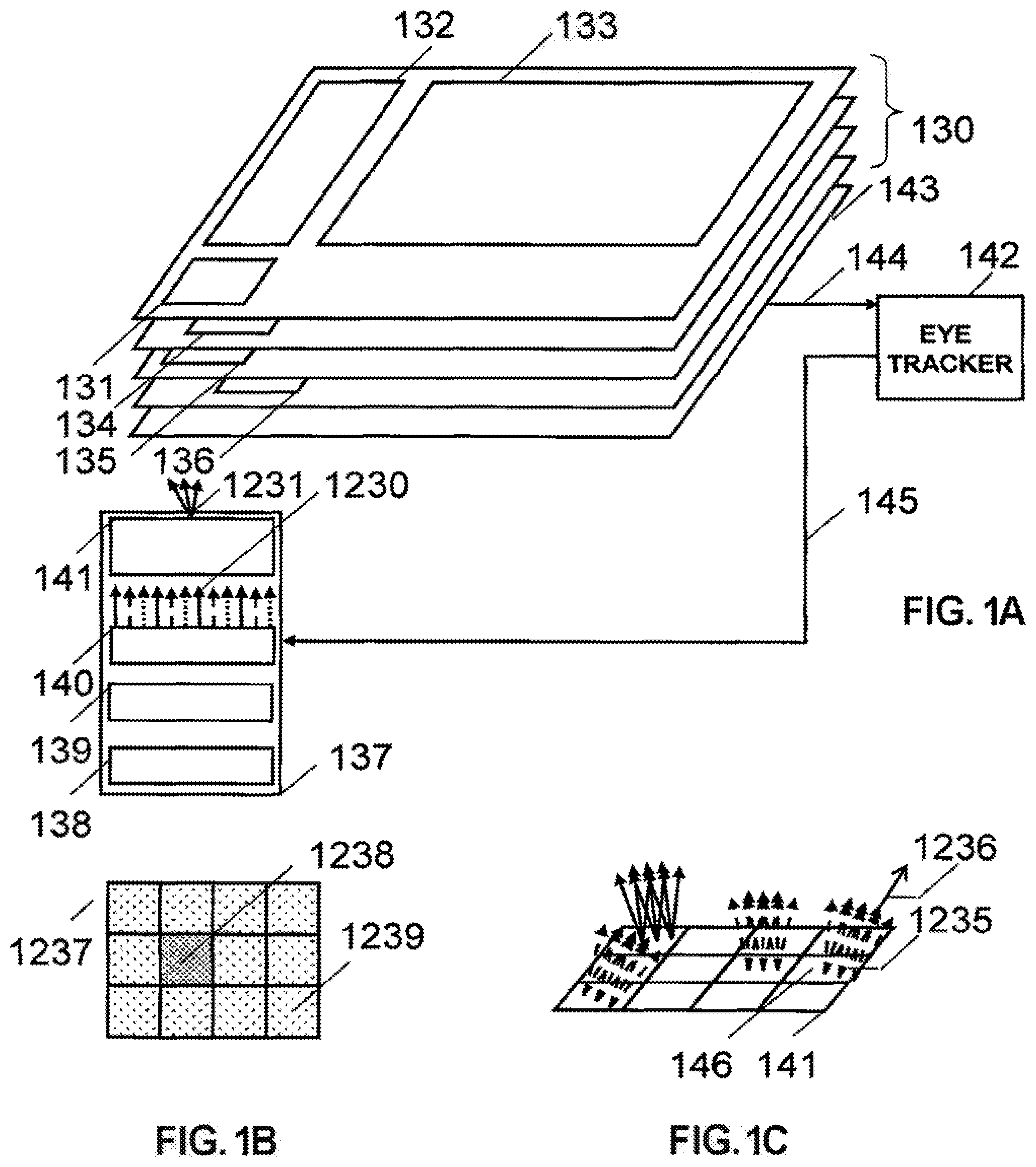
[0058] One important class of light field displays uses microlens array overlaying a spatial light modulator as disclosed in United States Patent Application Publication No.: US2014/0168783 by Luebke et al entitled NEAR-EYE MICROLENS ARRAY DISPLAYS. The following series of embodiments addresses how the microlens array scheme can be translated to a waveguide optical architecture with the goal of providing a thin transparent holographic waveguide light field display. The embodiment of FIG. 2 provides a monochrome light field display. FIG. 2A and FIG. 2B are cross sectional views of portions of the display. FIGS. 2C-2E are plan views. The display comprises an input waveguide 150 coupled to a microdisplay panel 151 on a backplane 152. The input waveguide contains a polarization-selective grating beamsplitter 153 the microdisplay, a waveguide despeckler 15 and a further grating 155 for in-coupling light from a source which may be a laser or LED die 156 on a backplane 157. FIG. 2B shows the light path from the source to the microdisplay as indicated by the rays 1250-1252 and the path of the reflected light 1253 from the microdisplay panel. Note that the grating 153 is polarization selection: in the case of a SBG high diffraction efficiency is obtained for P-polarization. The waveguide 160 contains fold grating comprising elements such as 161, an output grating array comprising elements such as 162-163 and input grating 165. In the embodiment shown a 1.times.3 fold grating array and a 3.times.3 output grating array are used. In one embodiment the waveguide also contains a thin beamsplitter homogenizer layer for vertical and horizontal homogenization. The input grating has high efficiency for maximum light in-coupling efficiency. In one embodiment output grating is a lossy grating for extracting light uniformly out of the waveguide along the beam path. In contrast to the input and output gratings which deflect light in a plane orthogonal to the waveguide the fold grating deflects light substantially in the plane of the waveguide. The elements of the two arrays are switching gratings (SBGs). The output grating array is overlaid by a holographic diffuser layer 166, holographic microlens array 167 and an eye tracker comprising separated waveguides for illumination 168 and detection 169. In one embodiment the holographic diffuser and microlens array are each recorded in a layer of HPDLC material sandwiched between transparent substrates. Desirably the microdisplay is of high resolution, ideally at least 2000.times.4000 pixels. Referring to FIG. 2E at any time on element of the fold grating array, for example 161 and one element of the adjacent row of output array elements, for example one of 162-163, is in its active (that is, diffracting) state. At the same time the microdisplay displays image information corresponding to a particular field of view region or tile. The active element diffracts the image light out of the waveguide 160 to form an image region on the holographic diffuser. In one embodiment the output gratings have lens power for focusing the image light onto the diffuser. In one embodiment the microdisplay is illuminated by a parallel beams formed by collimated optics disposed between the source and waveguide. The subsequent beam propagation from source to microdisplay and from microdisplay to the holographic diffuser is in collimated space with the image formed on the holographic diffuser having a resolution substantially equal to that of the microdisplay. In another embodiment an afocal magnifier is disposed along the optical path between the source and holographic diffuser to provide a larger effective pixel size on the holographic diffuser. By switching each element of the output grating in turn with the input image updated accordingly a composite image is provided at the holographic diffuser during an eye integration time. The subsequently imaging of this intermediate image by the microlens array forms the viewable light field image according to the well known principles of light field imaging.
[0059] The embodiment of FIG. 3 addresses the problem of implementing the embodiment of FIG. 2 in a full colour light field display. The embodiment of FIG. 3 provides a color light field display. FIG. 3A and FIG. 3C are cross sectional views of portions of the display. FIG. 3B and FIGS. 3D-3E are plan views. The display comprises an input waveguide 170 coupled to a microdisplay panel 171 on a backplane 176. The input waveguide contains red, green and blue polarization-selective grating beamsplitters 171A-171C the microdisplay 171, red green and blue waveguide despecklers 172-174 and red, green and blue gratings 175A-175C for in-coupling light from a source which may be a laser or LED die 177R-177G on a backplane 178. FIG. 3C shows the light path from the source to the microdisplay and the path of the reflected light from the microdisplay panel as indicated by the rays 1266-1267. The waveguide 180 comprises separate layers one of which as shown in plan view in FIG. 3E contains fold grating comprising elements such as 203, an output grating array comprising elements such as 204 and an input grating divided into the three regions 202A-202C. In the embodiment shown a 1.times.3 fold grating array and a 3.times.3 output grating array are used. In one embodiment the waveguide also contains a thin beamsplitter homogenizer layer for vertical and horizontal homogenization. The input grating has high efficiency for maximum light in-coupling efficiency. In one embodiment output grating is a lossy grating for extracting light uniformly out of the waveguide along the beam path. The elements of the two arrays are switching gratings (SBGs). The output grating array is overlaid by red, green and blue holographic diffuser layers 1193-195, and red, green and blue holographic microlens arrays 190-192 and an eye tracker comprising separated waveguides for illumination 198 and detection 199. In one embodiment the holographic diffuser and microlens array are each recorded in a layer of HPDLC material sandwiched between transparent substrates. Desirably the microdisplay is of high resolution, ideally at least 2000.times.4000 pixels. Referring to FIG. 3E at any time one element of the fold grating array, for example 203 and one element of the adjacent row of output array elements is in its active (that is, diffracting) state. At the same time the microdisplay displays image information corresponding to a particular field of view region or tile. The information is displayed in colour bands as illustrated in FIG. 3B which shows the illumination regions on the microdisplay 171A-171C correspond to the illumination color bands 175A-175C. In one embodiment the region 171A displays red information and is illumination by light from the illumination source region 175A. The red image light enters the waveguide 180 in the input grating region 202A which transmits the light into the fold grating where the active grating element 203 transmits the image to an active grating element in an adjacent row of the output grating. The region 205A of this element is illuminated by red image light which is deflected out of the waveguide into the holographic diffuser/holographic lens array stack. In one embodiment this above process is repeated cyclically for red, green and blue light, that is, only one color propagates at any time with each of the regions labeled A-C being illuminated by red, green and blue light. A more efficient process is to present red blue and green image information simultaneously. There for in one embodiment the illuminator provides red illumination in region 175A, green in 175B and blue in 175C while the microdisplay simultaneously display red image information in region 171A, green in 171B and blue in 171C. The active element of the output grating array then simultaneously outputs red image light in region 205A, green in 205B and blue in 205C.
[0060] The active element of the output grating army diffracts the image light out of the waveguide 180 to form red green and blue image region on the red green and blue holographic diffuser. In one embodiment the output gratings have lens power for focusing the image light onto the diffuser. In one embodiment the microdisplay is illuminated by a parallel beams formed by collimated optics disposed between the source and waveguide. The subsequent beam propagation from source to microdisplay and from microdisplay to the holographic diffuser is in collimated space with the image formed on the holographic diffuser having a resolution substantially equal to that of the microdisplay. In another embodiment an afocal magnifier is disposed along the optical path between the source and holographic diffuser to provide a larger effective pixel size on the holographic diffuser. By switching each element of the output grating in turn with the input image updated accordingly a composite image is provided at the holographic diffuser during an eye integration time. The subsequently imaging of this intermediate image by the red green and blue microlens arrays forms the viewable light field image according to the well known principles of light field imaging.
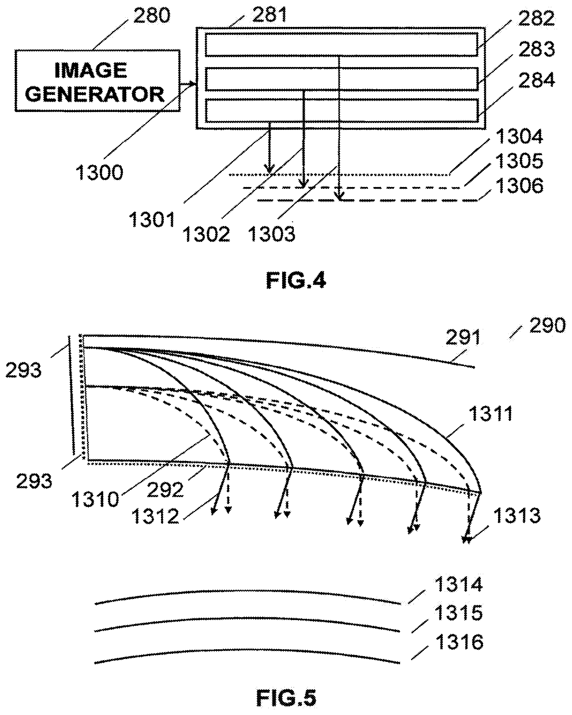
[0061] In one embodiment shown in FIG. 4 a light field display comprises an image generator 280 and a waveguide device 281 comprising multiple waveguide layers. Each layer contains at least one GRIN structure and at least one diffractive structure. Each waveguide layer provides a portion of the total field of view of the display. The display forms a light field as represented by the rays 1301-1303 and the image surfaces 1304-1306. The image generator may comprise a microdisplay panel or a scanner.
[0062] The above described embodiments may be used in conjunction with the GRIN embodiments disclosed in U.S. Provisional Application Ser. No. 62/125,066 entitled OPTICAL WAVEGUIDE DISPLAYS FOR INTEGRATION IN WINDOWS filed on 12 Jan. 2015. For example, in a wearable display application the GRIN embodiments may be used to relay image light from the image generator around a curved waveguide up to the grating waveguide devices.
[0063] FIG. 5 is a schematic side view of a GRIN waveguide 290 in embodiment of the invention comprising a curved GRIN substrate 291 having a curved output surface structure 292 and an input surface structure 293 which is in proximity to an intermediate focal surface. First and second ray paths through the GRIN medium are generally indicated by 1310 and 1311. The light beams refracted out of the output surface are generally indicated by 1312,1313. The waveguide forms a series of image surfaces 1314-16. The input surface structure 293 may be a microlens array formed using discrete refractive elements or a diffractive or holographic lens array. The input surface structure may comprise several layers. The output surface structure 292 may comprise a grating located on the output surface, within the GRIN waveguide or in a separate layer disposed in proximity to the output surface.
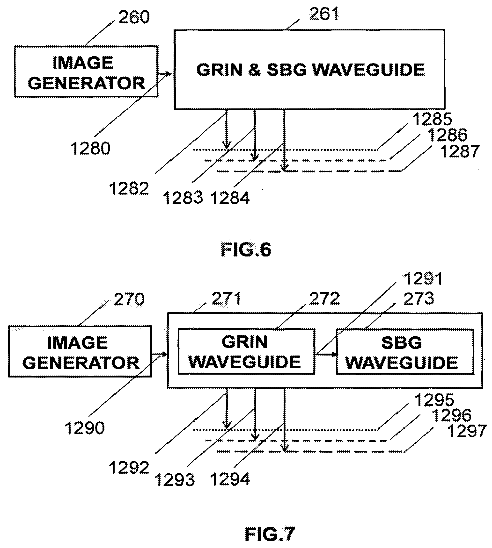
[0064] In one embodiment shown in FIG. 6 a light field display according to the principles of the invention comprises an image generator 260 and a waveguide device 261 in which are combined at least one GRIN structure and at least one grating structure. The display forms a light field as represented by the rays 1282-1284 and the image surfaces 1285-1287. The image generator may comprise a microdisplay panel or a scanner as disclosed above. In one embodiment shown in FIG. 7 a light field display according to the principles of the invention comprises an image generator 270 and a waveguide device 271 comprising a GRIN image relay waveguide and a grating. The display forms a light field as represented by the rays 1292-1294 and the image surfaces 1295-1297. The image generator may comprise a microdisplay panel or a scanner.
[0065] GRIN optics reproduces the optical properties of spherical lenses by gradual varying the refractive index of a material. In the most common application, GRIN fibers, the lens properties result from a radially varying index. Since the optical properties rely on the index distraction the input and output faces of a GRIN lens may be planar. GRIN lenses are manufactured by using various methods including neutron irradiation, chemical vapor deposition, ion exchange and partial polymerization, in which an organic monomer is partially polymerized using UV light at varying intensities. By precisely varying their refractive index, gradient index lenses are able to continuously bend light within the lens. This contrasts with conventional spherical lenses, which bend light only twice: when light meets the front surface of the lens and when it exits the back of the lens. Gradient index lenses can be positive (converging) or negative (diverging). GRIN lenses are capable of high quality imaging as demonstrated by their successful application in endoscopes.
[0066] GRIN waveguides several key advantages over TIR waveguides as used in the above-cited related patent applications, The first one is the GRIN eliminates the problem of banding. A major design challenge in waveguide optics is coupling the image content into the waveguide efficiently and in such a way the waveguide image is free from chromatic dispersion and brightness non uniformity. To overcome chromatic dispersion and to achieve the best possible collimation it is desirable to use lasers. However, lasers and other narrow band sources such as LEDs suffer from the problem of pupil banding artifacts which manifest themselves as output illumination non uniformity. Banding artifacts are formed when the collimated pupil is replicated (expanded) in a TIR waveguide. In very basic terms the light beams diffracted out of the waveguide each time the beam interacts with the grating have gaps or overlaps. This leads to an illumination ripple. The degree of ripple is a function of field angle, waveguide thickness, and aperture thickness. The effects are therefore most noticed in narrowband (e.g. laser) illumination sources. Banding can be smoothed by dispersion with broadband sources such as LEDs. However, current LEDs do not provide enough light output for waveguide displays. A second major benefit of GRIN waveguides is that the guided beams do not interact with the faces of the waveguide making the waveguides immune to external contaminants. Additional optical layers may be applied without interfering with the wave guiding. The third major benefit of GRIN is that curved waveguides can be engineered much more easily than with TIR waveguides.
[0067] A light field display according to the principles of the invention may be configured in many different ways including as a wearable display, a heads up display (HUD) or a head down display (HDD). The invention is applicable to displays of any size.
[0068] A display according to the principles of the invention may include a waveguide despeckler based on principles disclosed in PCT Application No.: PCT/GB2013/000500 entitled WAVEGUIDE FOR HOMOGENIZING ILLUMINATION, and U.S. Pat. No. 8,224,133 entitled LASER ILLUMINATION DEVICE both of which are incorporated herein by reference in their entireties.
[0069] It should be emphasized that the drawings are exemplary and that the dimensions have been exaggerated.
[0070] Any of the above-described embodiments may be implemented using plastic substrates using the materials and processes disclosed in PCT Application No.: PCT/GB2012/000680, entitled IMPROVEMENTS TO HOLOGRAPHIC POLYMER DISPERSED LIQUID CRYSTAL MATERIALS AND DEVICES. Advantageously, the switchable gratings are recorded in a reverse mode HPDLC material in which the diffracting state of the switchable grating occurs when an electric field is applied across the electrodes. An eye tracker based on any of the above-described embodiments may be implemented using reverse mode materials and processes disclosed in the above PCT application.
[0071] The method of fabricating the switchable gratings and the ITO electrodes used in any of the above-described embodiments of the invention may be based on the process disclosed in the PCT Application No. US2006/043938, entitled METHOD AND APPARATUS FOR PROVIDING A TRANSPARENT DISPLAY.
[0072] It should be understood by those skilled in the art that while the present invention has been described with reference to exemplary embodiments, it is to be understood that the invention is not limited to the disclosed exemplary embodiments. Various modifications, combinations, sub-combinations and alterations may occur depending on design requirements and other factors insofar as they are within the scope of the appended claims or the equivalents thereof.
* * * * *
References
D00000
D00001
D00002
D00003
D00004
D00005
XML
uspto.report is an independent third-party trademark research tool that is not affiliated, endorsed, or sponsored by the United States Patent and Trademark Office (USPTO) or any other governmental organization. The information provided by uspto.report is based on publicly available data at the time of writing and is intended for informational purposes only.
While we strive to provide accurate and up-to-date information, we do not guarantee the accuracy, completeness, reliability, or suitability of the information displayed on this site. The use of this site is at your own risk. Any reliance you place on such information is therefore strictly at your own risk.
All official trademark data, including owner information, should be verified by visiting the official USPTO website at www.uspto.gov. This site is not intended to replace professional legal advice and should not be used as a substitute for consulting with a legal professional who is knowledgeable about trademark law.