Integrated Filter Radiator For A Multiband Antenna
LE; Kevin
U.S. patent application number 16/753377 was filed with the patent office on 2020-10-22 for integrated filter radiator for a multiband antenna. The applicant listed for this patent is JOHN MEZZALINGUA ASSOCIATES, LLC. Invention is credited to Kevin LE.
| Application Number | 20200335881 16/753377 |
| Document ID | / |
| Family ID | 1000004943599 |
| Filed Date | 2020-10-22 |


View All Diagrams
| United States Patent Application | 20200335881 |
| Kind Code | A1 |
| LE; Kevin | October 22, 2020 |
INTEGRATED FILTER RADIATOR FOR A MULTIBAND ANTENNA
Abstract
Disclosed is a low band dipole that has four dipole arms in a cross configuration, and a simplified cloaking structure to substantially prevent interference with radiated RF energy from nearby high band dipoles. Further disclosed is a feed network and dipole stem balun configuration that power divides and combines two distinct RF signals, without the use of a hybrid coupler, so that the four dipole arms collectively radiate the two RF signals respectively at a +45 degree and -45 degree polarization orientation relative to the orientation of the dipole arms.
| Inventors: | LE; Kevin; (Bel Air, MD) | ||||||||||
| Applicant: |
|
||||||||||
|---|---|---|---|---|---|---|---|---|---|---|---|
| Family ID: | 1000004943599 | ||||||||||
| Appl. No.: | 16/753377 | ||||||||||
| Filed: | October 4, 2018 | ||||||||||
| PCT Filed: | October 4, 2018 | ||||||||||
| PCT NO: | PCT/US2018/054321 | ||||||||||
| 371 Date: | April 3, 2020 |
Related U.S. Patent Documents
| Application Number | Filing Date | Patent Number | ||
|---|---|---|---|---|
| 62567809 | Oct 4, 2017 | |||
| 62587926 | Nov 17, 2017 | |||
| Current U.S. Class: | 1/1 |
| Current CPC Class: | H01Q 1/38 20130101; H01Q 9/28 20130101; H01Q 1/521 20130101; H01Q 1/246 20130101; H01Q 21/26 20130101 |
| International Class: | H01Q 21/26 20060101 H01Q021/26; H01Q 9/28 20060101 H01Q009/28; H01Q 1/24 20060101 H01Q001/24; H01Q 1/38 20060101 H01Q001/38; H01Q 1/52 20060101 H01Q001/52 |
Claims
1. An antenna dipole, comprising: a first dipole arm that extends from a dipole center in a positive direction along a first axis; a second dipole arm that extends from the dipole center in a negative direction along the first axis; a third dipole arm that extends from the dipole center in a positive direction along a second axis, wherein the second axis is orthogonal to the first axis; a fourth dipole arm that extends from the dipole center in a negative direction along the second axis; a dipole stern on which the first, second, third, and fourth dipole arms are disposed, the dipole stem having a first dipole stem plate oriented along the first axis and a second dipole stem plate oriented along the second axis, the first and second dipole stem plates mechanically coupled in a cross arrangement having a center corresponding to the dipole center, the cross arrangement defining a first quadrant, a second quadrant, a third quadrant, and a fourth quadrant; and a feedline network having a +45 degree feedline and a -45 degree feedline, the +45 degree feedline having a +45 degree feedline power divider, a first +45 degree trace coupled to the +45 degree feedline power divider, and second +45 degree trace coupled to the +45 degree feedline power divider, the second +45 degree trace corresponding to a 180 degree phase delay relative to the first +45 degree trace, the -45 degree feedline having a -45 degree feedline power divider, a first -45 degree trace coupled to the -45 degree feedline power divider, and second -45 degree trace coupled to the -45 degree feedline power divider, the second -45 degree trace corresponding to a 180 degree phase delay relative to the first -45 degree trace, wherein the first +45 degree trace is coupled to a first balun disposed on the first stem plate in the fourth quadrant, the second +45 degree trace is coupled to a second balun disposed on the first stem plate in the first quadrant, the first -45 degree trace is coupled to a third balun disposed on the second stem plate in the third quadrant, and the second -45 degree trace is coupled to a fourth balun disposed on the second stem plate in the second quadrant.
2. The antenna dipole of claim 1, wherein the first balun is coupled to a first ground plate disposed on the second stem plate in the fourth quadrant, the second balun is coupled to a second ground plate disposed on the second stem plate in the first quadrant, the third balun is coupled to a third ground plate disposed on first stern plate in the third quadrant, and the fourth balun is coupled to a fourth around plate disposed on the first stein plate in the second quadrant.
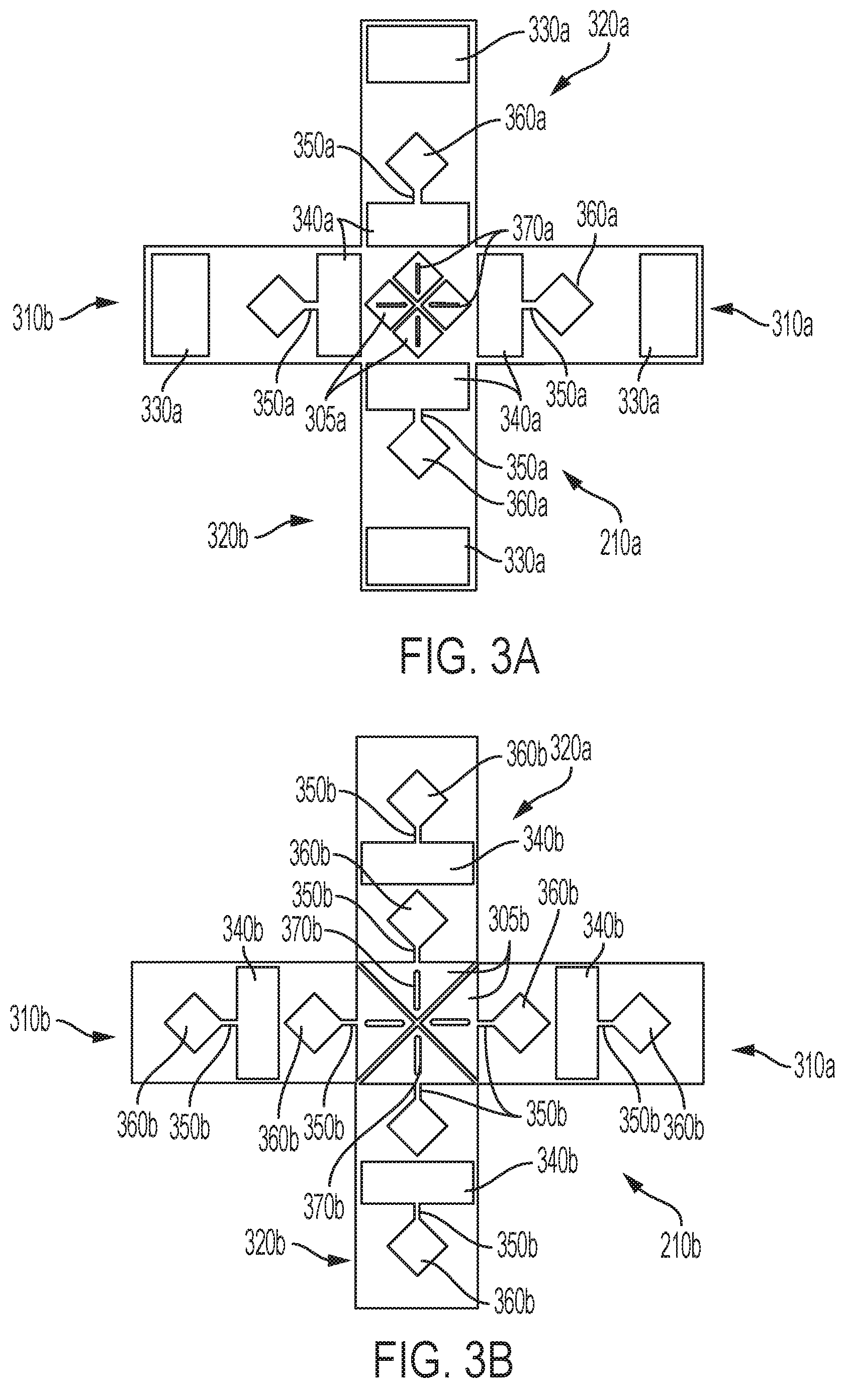
3. The antenna dipole of claim 2, wherein the first ground plate is coupled to the fourth dipole arm, the second ground plate is coupled to the third dipole arm, the third ground plate is coupled to the second dipole arm, and the fourth ground plate is coupled to the first dipole arm.
4. The antenna dipole of claim 3, wherein the +45 degree feedline is coupled to a first RF signal, and wherein the -45 degree feedline is coupled to the first RF signal having a 90 degree phase delay.
5. A dipole, comprising: four dipole arms arranged in a cross configuration; and a dipole stem having a plurality of microstrip baluns and microstrip ground plates disposed thereon, wherein each of the microstrip ground plates is coupled to a corresponding dipole arm, wherein the microstrip baluns and microstrip ground plates are arranged such that each microstrip ground plate receives a directly coupled RF signal corresponding to one of a +45 degree polarization signal and a -45 degree polarization signal and a capacitively coupled RF signal corresponding to the other of the +45 degree polarization signal and the -45 degree polarization signal.
6. A dipole, comprising: a PCB substrate; a first plurality of cloaking elements disposed on a first side of the PCB substrate; and a second plurality of cloaking elements disposed on a second side of the PCB substrate, wherein the first plurality of cloaking elements and the second plurality of cloaking elements are respectively formed from a single conductive layer respectively disposed on the first and second side of the PCB substrate.
7. The dipole of claim 6, wherein the first plurality of cloaking elements comprises a sequence of a first conductive element, a first inductor, and a first capacitor plate, and wherein the second plurality of cloaking elements comprises a sequence of a second inductor, a second capacitor plate, a gap, and a second conductive element, wherein the first capacitor plate and the second conductive element are disposed opposite each other on the PCB substrate.
8. The dipole of claim 7, wherein the first conductive element and the second capacitor plate are disposed opposite each other on the PCB substrate.
Description
BACKGROUND OF THE INVENTION
Field of the Invention
[0001] The present invention relates to antennas for wireless communications, and more particularly, to multiband antennas that have low band and high band dipoles located in close proximity.
Related Art
[0002] There is considerable demand for cellular antennas that can operate in multiple bands and at multiple orthogonal polarization states to make the most use of antenna diversity. A solution to this is to have an antenna that operates in two orthogonal polarization states in the low band (LB) (e.g., 496-690 MHz) and in two orthogonal polarization states in the high band (HB) (e.g., 1.7-3.3 GHz). There is further demand for the antenna to have minimal wind loading, which means that it must be as narrow as possible to present a minimal cross-sectional area to oncoming wind.
[0003] The need for a compact array face for an antenna that operates in both the low band and the high band presents challenges. Specifically, the more closely LB and HB dipoles are spaced on a single array face, the more they suffer from interference whereby transmission in either the HB and harmonics of the LB is respectively picked up by the dipoles of the other band, causing coupling and re-radiation that contaminates the gain pattern of the transmitting band.
[0004] This problem can be solved with dipoles that are designed to be "cloaked", whereby they radiate and receive in the band for which they are designed yet are transparent to the other band that is radiated by the other dipoles sharing the same compact array face. However, it can be costly to manufacture cloaked dipoles, which may require additional layers of components and rather complex structures.
[0005] FIGS. 1a and 1b illustrate an antenna array face 100 with a plurality of HB dipoles 110 and an LB dipole 120. As illustrated, both LB and HB dipoles may both operate in +/-45.degree. polarizations, enabling two HB signals and two LB signals to operate simultaneously. As may be inferred from FIGS. 1a and 1b, LB dipole 120 may physically obstruct one or more HB dipoles 110, leading to cross-band contamination and degrading the HB gain pattern.
[0006] Further, there is also demand for cellular antennas that are capable of operating in circular polarization in the low band. This offers greatly improved performance, but generally requires completely different dipole hardware in order to implement it, making a full scale deployment of a circular polarized low band communication scheme cost prohibitive.
[0007] Accordingly, what is needed is a low band dipole configuration that minimizes physical interference and cross coupling with nearby high band dipoles, is capable of being operated simultaneously in +/-45.degree. polarization states, is capable of being operated in a circular polarization mode without requiring hardware modifications, and is inexpensive and easy to manufacture.
SUMMARY OF THE INVENTION
[0008] Accordingly, the present invention is directed to an integrated filter radiator for multiband antenna that obviates one or more of the problems due to limitations and disadvantages of the related art.
[0009] An aspect of the present invention involves an antenna dipole that comprises a first dipole arm that extends from a dipole center in a positive direction along a first axis; a second dipole arm that extends from the dipole center in a negative direction along the first axis; a third dipole arm that extends from the dipole center in a positive direction along a second axis, wherein the second axis is orthogonal to the first axis; and a fourth dipole arm that extends from the dipole center in a negative direction along the second axis. The antenna further comprises a dipole stem on which the first, second, third, and fourth dipole arms are disposed. The dipole stein has a first dipole stem plate oriented along the first axis and a second dipole stem plate oriented along the second axis, the first and second dipole stem plates mechanically coupled in a cross arrangement having a center corresponding to the dipole center, the cross arrangement defining a first quadrant, a second quadrant, a third quadrant, and a fourth quadrant. The antenna also has and a feedline network having a +45.degree. feedline and a -45.degree. feedline. The +45.degree. feedline has a +45.degree. feedline power divider, a first +45.degree. trace coupled to the +45.degree. feedline power divider, and second +45.degree. trace coupled to the +45.degree. feedline power divider, the second +45.degree. trace corresponding to a 180.degree. phase delay relative to the first +45.degree. trace. The -45.degree. feedline has a -45.degree. feedline power divider, a first -45.degree. trace coupled to the -45.degree. feedline power divider, and second -45.degree. trace coupled to the -45.degree. feedline power divider, the second -45.degree. trace corresponding to a 180.degree. phase delay relative to the first -45.degree. trace, wherein the first +45.degree. trace is coupled to a first balun disposed on the first stem plate in the fourth quadrant, the second +45.degree. trace is coupled to a second balun disposed on the first stem plate in the first quadrant, the first -45.degree. trace is coupled to a third balun disposed on the second stein plate in the third quadrant, and the second -45.degree. trace is coupled to a fourth balun disposed on the second stem plate in the second quadrant.
[0010] Another aspect of the present invention involves a dipole that comprises four dipole arms arranged in a cross configuration, and a dipole stem having a plurality of microstrip baluns and microstrip ground plates disposed thereon, wherein each of the microstrip ground plates is coupled to a corresponding dipole arm, wherein the microstrip baluns and microstrip ground plates are arranged such that each microstrip ground plate receives a directly coupled RF signal corresponding to one of a +45.degree. polarization signal and a -45.degree. polarization signal and a capacitively coupled RF signal corresponding to the other of the +45.degree. polarization signal and the -45.degree. polarization signal.
[0011] Yet another aspect of the present invention involves a dipole that comprises a PCB substrate; a first plurality of cloaking elements disposed on a first side of the PCB substrate; and a second plurality of cloaking elements disposed on a second side of the PCB substrate, wherein the first plurality of cloaking elements and the second plurality of cloaking elements are respectively formed from a single conductive layer respectively disposed on the first and second side of the PCB substrate. Further embodiments, features, and advantages of the integrated filter radiator for multiband antenna, as well as the structure and operation of the various embodiments of the integrated filter radiator for multiband antenna, are described in detail below with reference to the accompanying drawings.
[0012] It is to be understood that both the foregoing general description and the following detailed description are exemplary and explanatory only, and are not restrictive of the invention as claimed
BRIEF DESCRIPTION OF THE DRAWINGS
[0013] The accompanying drawings, which are incorporated in and constitute a part of this specification, illustrate embodiment(s) of the integrated filter radiator for multiband antenna described herein, and together with the description, serve to explain the principles of the invention.
[0014] FIGS. 1a and 1b illustrate an antenna array face having diagonally oriented HB and LB dipoles for operation in +/-45.degree. polarizations.
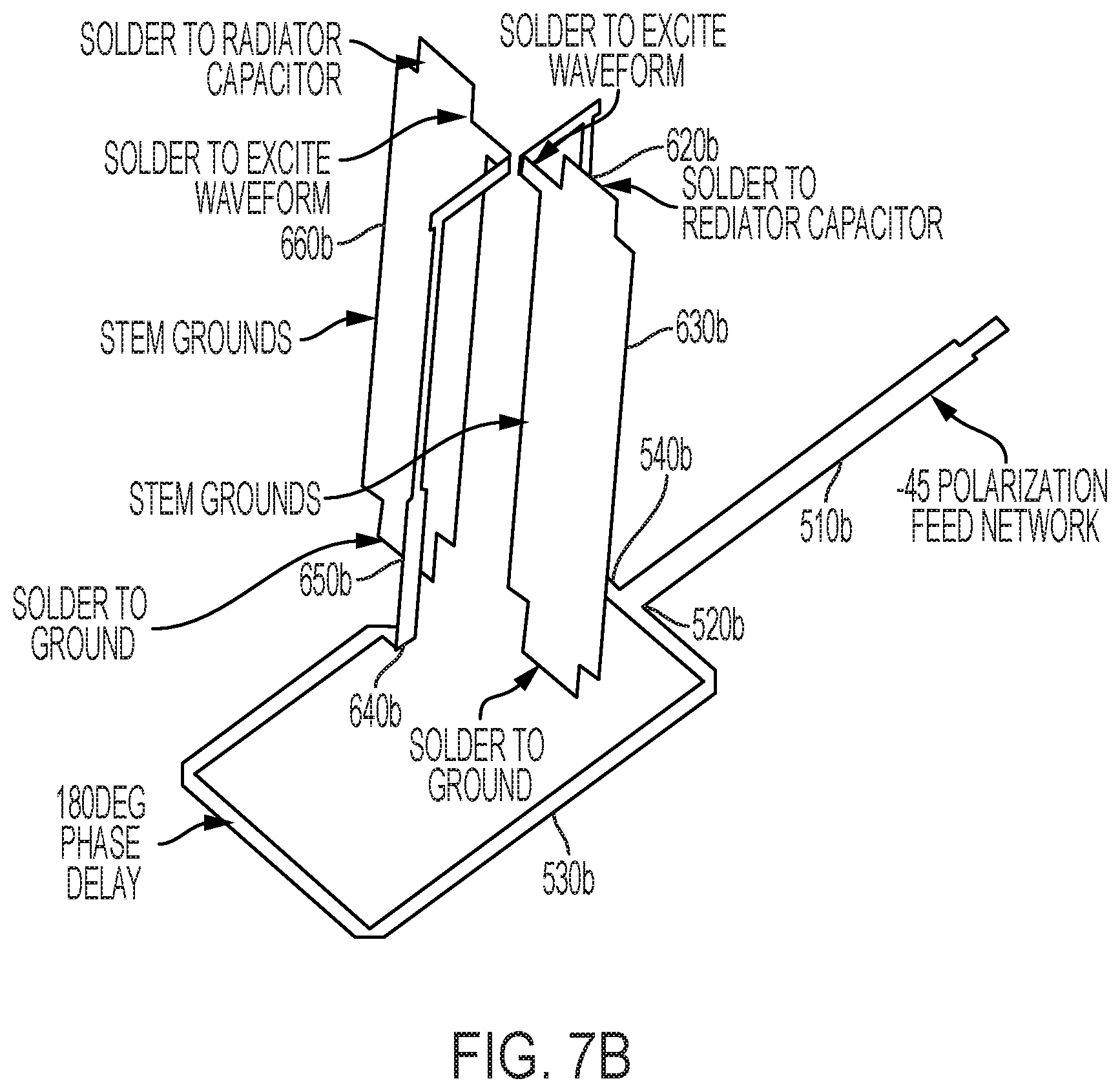
[0015] FIGS. 2a and 2b illustrate an exemplary antenna array face in which the LB dipole is oriented in a vertical acid horizontal orientation yet operates in +/-45.degree. polarizations.
[0016] FIG. 3a illustrates a top or front surface of an exemplary LB dipole according to the disclosure.
[0017] FIG. 3b illustrates a bottom or back surface of an exemplary LB dipole according to the disclosure.
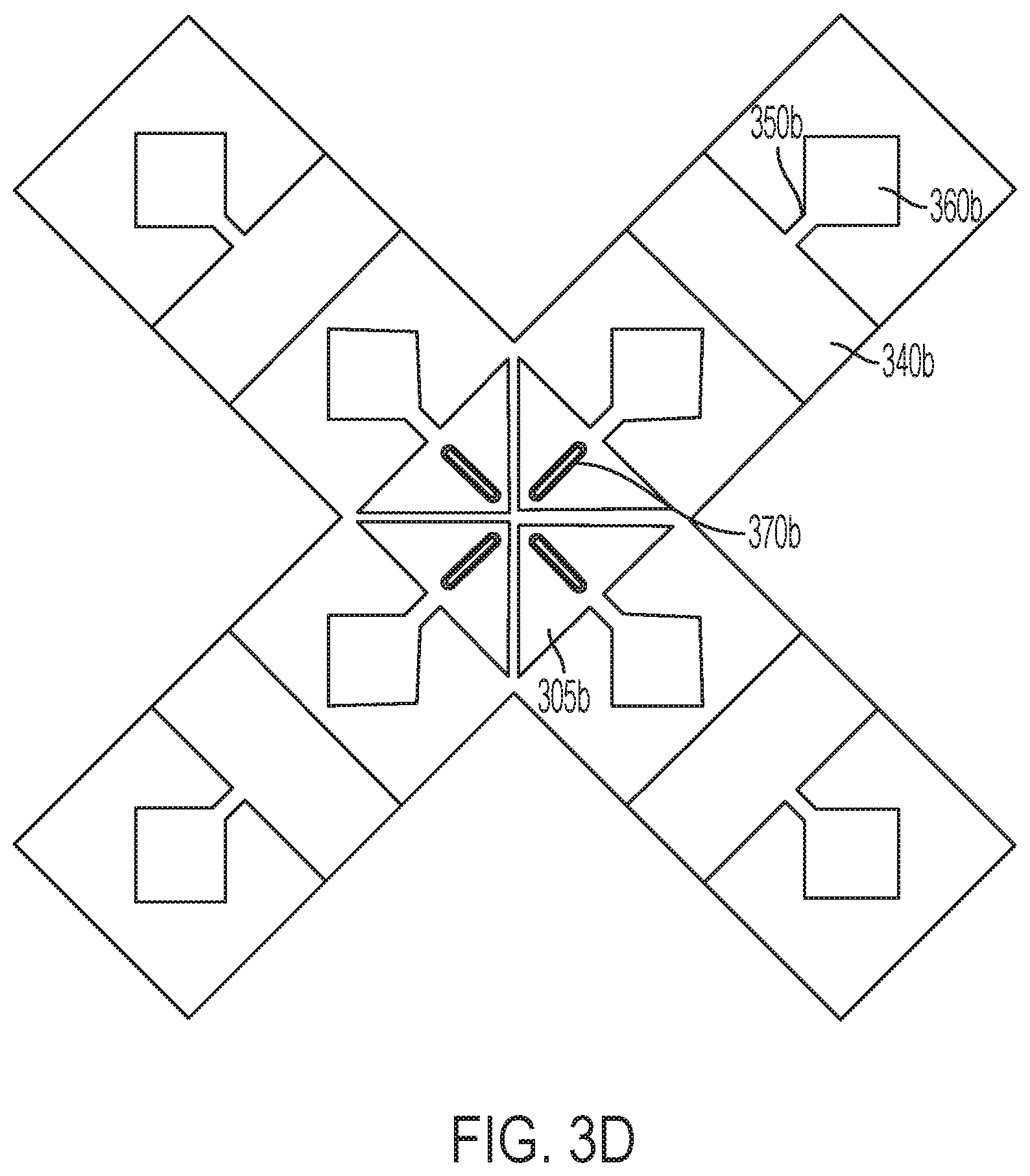
[0018] FIG. 3c illustrates the top or front surface of the LB dipole, showing exemplary dimensions.
[0019] FIG. 3d illustrates the bottom or back surface of the LB dipole, showing exemplary dimensions.
[0020] FIG. 4 illustrates a side view of an exemplary LB dipole according to the disclosure, revealing the arrangement of conductive elements on the top and bottom surfaces of a PCB substrate.
[0021] FIG. 5 illustrates an exemplary LB dipole according to the disclosure, including its dipole stem and portions of the feedline network.
[0022] FIG. 6a illustrates the LB dipole stem from a "top-down" perspective, along with the balun circuit and relevant feedlines for an exemplary +45.degree. polarization LB dipole component.
[0023] FIG. 6b illustrates the LB dipole stem from a "top-down" perspective, along with the balun circuit and relevant feedlines for an exemplary -45.degree. polarization LB dipole component.
[0024] FIG. 6c illustrates the LB dipole stem, similarly to FIGS. 6a and 6b, with the balun circuitry for both +45.degree. and -45.degree. polarizations present on the dipole stem.
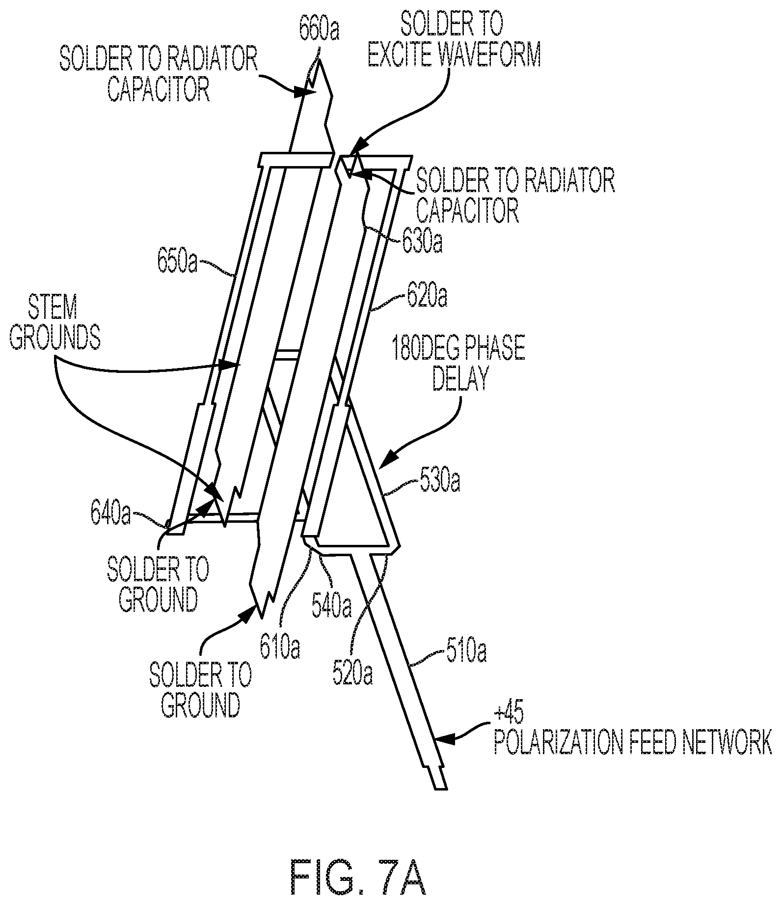
[0025] FIG. 7a is a different perspective view of the feedlines and balun circuit for the +45.degree. polarization LB dipole component.
[0026] FIG. 7b is a different perspective view of the feedlines and balun circuit for the -45.degree. polarization LB dipole component.
[0027] FIG. 8 illustrates the balun circuitry for both the +45.degree. and -45.degree. polarization components of the LB dipole, with the dipole stem plates removed from view.
[0028] FIG. 9 illustrates the balun circuitry of FIG. 8, but with the dipole stem plates in view.
[0029] FIG. 10a illustrates the top and bottom sides of an additional exemplary LB dipole.
[0030] FIG. 10b illustrates the exemplary LB dipole of FIG. 10a, along with a depiction of the capacitive and inductive structures embedded within the dipole structure
[0031] FIG. 11 illustrates the top and bottom sides of another exemplary LB dipole, having a reduced LB dipole span.
[0032] FIG. 12 plots S-parameter performance of the LB dipole illustrated in FIG. 11.
DESCRIPTION OF EXEMPLARY EMBODIMENTS
[0033] Reference will now be made in detail to embodiments of the integrated filter radiator for multiband antenna with reference to the accompanying figures
[0034] FIGS. 2a and 2b illustrate an exemplary antenna array face in which the HB dipoles 110 are oriented diagonally, and the LB dipole 210 is oriented in a vertical and horizontal direction yet is configured top radiate and receive in +/-45.degree. polarizations. As illustrated, having the LB dipole 210 oriented vertically and horizontally substantially mitigates the physical obstruction present in the antenna array face of FIGS. 1a and 1b. As is described below, LB dipole 210 has a vertically-oriented LB dipole and a horizontally-oriented dipole. The vertically-oriented dipole has a radiator component extending "upward" from center that is fed by an individual LB RF feed (not shown), and a counterpart radiator component extending "downward" from center that is fed by another LB RF feed (also not shown). Similarly, the horizontally-oriented LB dipole has a radiator component extending "leftward" from center that is fed by an individual LB RF feed (not shown), and a counterpart radiator component extending "rightward" from center that is fed by another LB RF feed (also not shown). These dipole structures are described in further detail in FIGS. 3a and 3b.
[0035] It will be understood that the terms "upward" and "downward" are used for convenience in reference to the drawings, and do not refer to the actual orientation of the LB dipole 210.
[0036] FIGS. 3a and 3b respectively illustrate a front or "top" face 210a of LB dipole 210, and a back or "bottom" face 210b of LB dipole 210. Both figures illustrate a first horizontal dipole arm 310a that extends "rightward" from the dipole center, second horizontal dipole arm 310b that extends "leftward" from the dipole center, a first vertical dipole arm 320a that extends "upward" from the dipole center, and second vertical dipole arm 320b that extends "downward" from the dipole center. As illustrated, the shaded portions of front face 210a and back face 210b correspond to PCB substrate or an otherwise non-conducting surface, and the non-shaded portions correspond to metal conductor, such as copper.
[0037] Referring to FIG. 3a, at the center region of the cross shape of front dipole face 210a are four solder pads 305a to which corresponding microstrip ground plates (described later) are conductively coupled, and which are surrounded by non-conductive surface. Moving outward from center along each dipole arm, the next component in each dipole arm is a conductive element 340a, coupled to which is an "outward" facing inductor trace 350a to which is coupled a "diamond" shaped capacitive element 360a. Conductive element 340a, inductor trace 350a, and capacitive element 360a may be formed of a single piece of metal, such as copper. Located further "outward" is a distal conductive element 330a, which is separated from its corresponding diamond shaped capacitive element 360a by a gap. Exemplary dimensions are shown in FIG. 3c.
[0038] Referring to FIG. 3b, at the center region of the cross shape of back dipole face 210b are four "arrowhead" conductive elements 305b, each corresponding to an arm of the back dipole face 210b. Within each arrowhead conductive element 305b is a via 370b, through which microstrip ground plates (described later) pass without making conductive contact to arrowhead conductive element 305b. This may be accomplished whereby the conductive portion of the microstrip ground plate has disposed on it a solder mask, which prevents electrically conductive contact between microstrip ground plate and arrowhead conductive element 305b. Moving outward from center along each dipole arm, each arrowhead conductive element 305a is coupled to an inductor trace 350b, which is in turn coupled to a "diamond" shaped capacitive element 360b. Located further outward is conductive element 340b, which is separated from diamond shaped capacitive element 360b by a gap and which is coupled to further inductor trace 350b, to which is coupled a further diamond shaped capacitive element 360b.
[0039] Although capacitive element 360a/b has a "diamond" shape in this example, other shapes (e.g., rectangular, triangular, circular, etc.) are possible and within the scope of the disclosure, as long as the volume of the capacitive element is the same.
[0040] FIGS. 3c and 3d respectively illustrate front face 210a and back face 210b of LB dipole 210, including exemplary dimensions. It will be readily understood that these dimensions are examples, and that varying dimensions are possible and within the scope of the disclosure.
[0041] FIG. 4 illustrates a side view of an exemplary LB dipole 210 according to the disclosure, revealing the arrangement of conductive elements on the top and bottom surfaces (respectively, front face 210a and back face 210b). LB dipole 210 includes a PCB substrate 410, and a conductive surface on the top and bottom that may be etched to form the components of front face 210a and back face 210b. As illustrated, dipole stein 400 engages LB dipole 210 by mechanically coupling directly to back face 210b, and microstrip ground plates (described later) electrically and mechanically couple to front face 210a by being passed through via 370b (of back face 210b) and soldered to solder pad 305a (of front face 210a). Further illustrated in FIG. 4 are the alternating combinations of conductive elements 340a and 330a (on front face 210a) in back-to-back configurations with corresponding diamond shaped capacitive elements 360b (on back face 210b), as well as conductive elements 340b (on back face 210b) in a back-to-back configuration with diamond shaped capacitive element 360a (on front face 210a). Accordingly, a plurality of capacitors are formed. A first capacitor is formed of conductive element 340a and its corresponding capacitive element 360b, with the PCB substrate 410 serving as the dielectric; a second capacitor is formed of conductive element 340b and its corresponding capacitive element 360a, with the PCB substrate 410 serving as its dielectric; and a third capacitor is formed of conductive element 330a and its corresponding capacitive element 360b, with the PCB substrate 410 serving as its dielectric. Accordingly, each dipole arm assembly 310a/b and 320a/b comprises a succession of capacitors and inductors, providing a cloaking function whereby RF energy radiated by the HB dipoles are effectively transparent to the LB dipole, and induced currents are suppressed, thus mitigating interference between the HB and LB dipoles.
[0042] Exemplary materials for the LB dipole 210 may include the following. Substrate 410 may be a standard PCB material, such as 0.0203'' Rogers 4730JXR, and the conductive material disposed on the top and bottom surfaces of substrate 410 (which may be etched to form the illustrated components) may by 1 oz. copper. It will be understood that variations to these materials are possible and within the scope of the disclosure.
[0043] The structure of LB dipole 210 offers an advantage in that it comprises a single PCB substrate on which a conductive layer is disposed. The conductive layer on the front and back faces of the dipole may be etched to form the structure disclosed. Accordingly, the structure of LB dipole 210 is extremely simple and inexpensive to manufacture, unlike other cloaked dipole configurations.
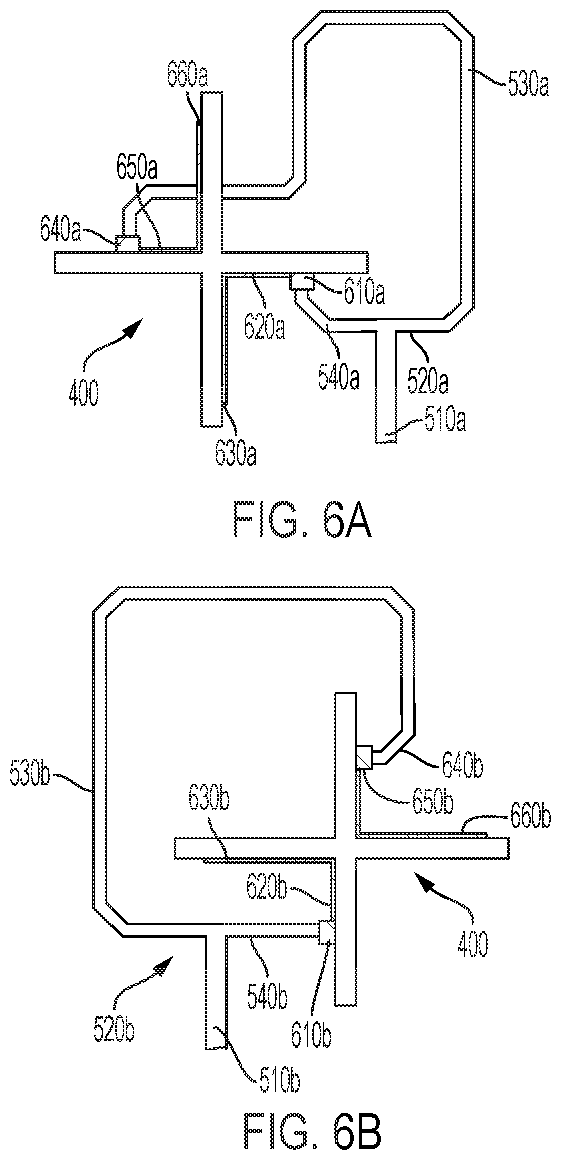
[0044] FIG. 5 illustrates exemplary LB dipole 210, mounted on dipole stem 400, and a portion of the feed network disposed on a feedboard to which the dipole stem 400 is mounted. The feed network includes RF feedlines corresponding to the +45.degree. signal and the -45.degree. signal. Illustrated is +45.degree. feedline 510a, which includes a power divider 520a, and two traces coupled to the power divider 520a: first +45.degree. trace 540a, and second -45.degree. trace 530a. First +45.degree. trace 540a couples directly to a microstrip balun that feeds corresponding dipole arm 310a. Second +45.degree. trace 530a takes a longer path to couple with a microstrip balun such that the RF signal that reaches the other microstrip balun is 180.degree. out of phase with the signal on trace 540a where it couples with its corresponding microstrip balun. Further illustrated is -45.degree. feedline 510b, which includes a power divider 520b and two traces coupled to power divider 520b: first -45.degree. trace 540b and second -45.degree. trace 530b.
[0045] FIG. 6a illustrates the LB dipole stein 400 from a "top-down" perspective, along with the baton circuit and relevant feedlines for an exemplary +45.degree. polarization LB dipole signal. This perspective is looking "down" on the dipole stem 400 with the LB dipole 210 removed, such that the dipole stem 400 would be coming out perpendicularly out of the page. Illustrated are +45.degree. signal feedline 510a, power divider 520a, and first trace 540a. First trace 540a couples directly to microstrip balun 620a at connection point 610a, whereby microstrip balun 620a is electrically coupled to corresponding microstrip ground plate 630a, which is disposed on the proximal surface of the stein plate orthogonal to the stem plate on which microstrip balun 620a is disposed as it traces from connection point 610a. Second trace 530a proceeds from power divider 520a and meanders before electrically coupling to opposite microstrip balun 650a via connection point 640a such that the signal arriving at connection 640a has a 180.degree. phase delay relating to the signal arriving at connection point 610a. Microstrip balun 650a further couples to opposite microstrip ground plate 660a, which is disposed on the dipole stem plate orthogonal to the dipole stem plate on which connection point 640a is disposed.
[0046] FIG. 6b illustrates the LB dipole stem 400 at the same orientation as in FIG. 6a. However, FIG. 6b illustrates the feedline and balun circuitry for the -45.degree. polarization LB dipole signal. Illustrated are -45.degree. signal feedline 510b, power divider 520b, and first trace 540b. First trace 540b couples directly to microstrip balun 620b at connection point 610b, whereby microstrip balun 620b electrically couples to corresponding microstrip ground plate 630b, which is disposed on a stem plate orthogonal to the stem plate on which microstrip balun is disposed as it traces from connection point 610b. Second trace 530b proceeds from power divider 520b and meanders before electrically coupling to opposite microstrip balun 650b via connection point 640b such that the signal arriving at connection 640b has a 180.degree. phase delay relating to the signal arriving at connection point 610b. Microstrip balun 650b further couples to opposite microstrip ground plate 660b, which is disposed on the dipole stem plate orthogonal to the dipole stem plate on which connection point 640b is disposed.
[0047] Referring back to FIG. 5, it will be apparent that the microstrip baluns 620a, 650a, 620b, and 650b substantially span the distance from respective connection points 610a, 640a, 610b and 640b upward to near the base of dipole arms 310a/b and 320a/b. Further, microstrip ground plates 630a, 660a, 630b, and 660b are each electrically coupled to a ground plane (not shown) in the multilayer PCB board to which dipole stem 400 is affixed.
[0048] FIG. 6c illustrates the LB dipole stem, similarly to FIGS. 6a and 6b, with the balun circuitry for both +45.degree. and -45.degree. polarizations illustrated on the dipole stem. But first, some background.
[0049] It is known that two dipoles arms, oriented horizontally and vertically, with each dipole arm having a single RF feed, can be configured to radiate at +/-45 degree polarization orientations, through the use of hybrid couplers. There are several considerable drawbacks to this approach. First, each hybrid coupler incurs a 3 dB loss on each signal. Second, the hybrid coupler has limited isolation, which degrades the performance of the dipole in radiating two distinct RF signals at different polarizations. The structure according to the disclosure does not suffer these disadvantages.
[0050] Referring to FIG. 6c, illustrated are the four microstrip baluns, each corresponding to a polarization and a phase delay: 620a (+45.degree./0.degree.); 650a (+45.degree./180.degree.); 620b (-45.degree./0.degree.); and 650b (-45.degree./180.degree.); and the four microstrip ground plates: 630a (+45.degree./0.degree., directly coupled to microstrip balun 620a); 660a (+45.degree./180.degree., directly coupled to microstrip balun 650a); 630b (-45.degree./0.degree., directly coupled to microstrip balun 620b); and 660b (-45.degree./180.degree., directly coupled to microstrip balun 650b). The microstrip baluns are respectively coupled to their corresponding microstrip ground plates by making a 90.degree. bend from the stem plate surface on which the microstrip balun is disposed to the proximal surface of the orthogonal stem plate.
[0051] Referring to FIGS. 6c and 3a, and 3b, microstrip ground plate 660b is coupled to dipole arm 310a as follows. Dipole stem 400 as four tabs (not shown) that pass through vias 570b (FIG. 3b). Microstrip ground plate 660b, as it is disposed on dipole stem plate 400, has a conductive tab that extends through its corresponding via 370b where it is electrically coupled (e.g., soldered) to its corresponding solder pad 305a on dipole arm 310a. Similarly, microstrip ground plate 630b is coupled to dipole arm 310b through a similar arrangement. Further, microstrip ground plate 660a is coupled to dipole arm 320a, and microstrip ground plate 630b is coupled to dipole arm 320b by corresponding arrangements.
[0052] Another way to visualize FIG. 6c is to divide the configuration into quadrants, whereby the top left (first) quadrant includes microstrip balun 650a and microstrip ground plate 660a; the top right (second) quadrant includes microstrip balun 650b and microstrip ground plate 660b; the bottom left (third) quadrant includes microstrip balun 620b and microstrip ground plate 630b; and the bottom right (fourth) quadrant includes microstrip balun 620a and microstrip ground plate 630a.
[0053] The configuration of microstrip baluns and microstrip ground plates is as follows. Each microstrip ground plate conducts two independent currents. One current is directly sourced from the microstrip balun to which it is directly coupled, and the other is capacitively coupled from the microstrip balun disposed on the opposite side of the stem plate on which the microstrip ground plate is disposed.
[0054] For example, referring to FIG. 6c, for the +45.degree. polarization and 0.degree. phase signal, the signal couples from connection point 610a to microstrip balm 620a. The current on microstrip balun 620a capacitively couples to microstrip ground plate 660b, through which the resulting current couples to dipole arm 310a. Additionally, the current in microstrip balun 620a flows directly to microstrip ground plate 630a, through which it couples to dipole arm 320b. Given the tuning of the balun circuitry between microstrip balun 620a, and microstrip ground plates 660b and 630a, a substantially equal current is respectively induced in dipole aims 310a and 320b. This results in a radiated waveform with its polarization vector oriented at +45.degree., with the rightward and downward signals respectively serving as vector components of the +45.degree. polarization vector.
[0055] A similar process occurs for the +45.degree. signal with 180.degree. phase delay. In this case, the phase delayed signal couples from connection point 640a to microstrip balun 650a. The current on microstrip balun 650a capacitively couples to microstrip ground plate 630b, through which the resulting current couples to dipole arm 310b. Additionally, the current in microstrip balun 650a flows directly to microstrip ground plate 660a, through which it couples to dipole arm 320a. Given the tuning of the balun circuitry between microstrip balun 640a, and microstrip ground plates 630b and 660a, a substantially equal current is respectively induced in dipole arms 310b and 320a. This results in a radiated waveform with its polarization vector oriented at +45.degree., with the leftward and upward signals respectively serving as vector components of the +45.degree. polarization vector.
[0056] The two +45.degree. polarization signals, being 180.degree. out of phase from each other, given the configuration of the baluns and the dipoles, results in a constructive interference of the two emitted RF waveforms, doubling the amplitude of the radiated energy of just one of the +45.degree. signal components.
[0057] The mode of operation is similar for the -45.degree. signals. Referring to FIG. 6c, for the -45.degree. polarization and 0.degree. phase signal, the signal couples from connection point 610b to microstrip balun 620b. The current on microstrip balun 620b capacitively couples to microstrip ground plate 630a, through which the resulting current couples to dipole arm 320b. Additionally, the current in microstrip balun 620b flows directly to microstrip ground plate 630b, through which it couples to dipole arm 310b. Given the tuning of the balun circuitry between microstrip balun 620b, and microstrip ground plates 630a and 630b, a substantially equal current is respectively induced in dipole arms 310b and 320b. This results in a radiated waveform with its polarization vector oriented at -45.degree., with the leftward and downward signals respectively serving as vector components of the -45.degree. polarization vector.
[0058] A similar process occurs for the -45.degree. signal with 180.degree. phase delay. In this case, the phase delayed signal couples from connection point 640b to microstrip balun 650b. The current on microstrip balun 650b capacitively couples to microstrip ground plate 660a, through which the resulting current couples to dipole arm 320a. Additionally, the current in microstrip balun 650b flows directly to microstrip ground plate 660b, through which it couples to dipole arm 310a. Given the tuning of the balun circuitry between microstrip balun 640b, and microstrip ground plates 660a and 660b, a substantially equal current is respectively induced in dipole arms 310a and 320a. This results in a radiated waveform with its polarization vector oriented at -45.degree., with the rightward and upward signals respectively serving as vector components of the -45.degree. polarization vector.
[0059] The two -45.degree. polarization signals, being 180.degree. out of phase from each other, given the configuration of the baluns and the dipoles, results in a constructive interference of the two emitted RF waveforms, doubling the amplitude of the radiated energy of just one of the -45.degree. signal components.
[0060] Accordingly, instead of relying on hybrid couplers for splitting and combining the two RF signals, the feed network and balun configuration of the present disclosure splits and recombines the appropriate signals by superimposing two signals into each microstrip capacitor plate and thus to each arm of the LB dipole, creating orthogonal vertical and horizontal polarization vector components for each of the RF signals, thereby generating +/-45.degree. polarization signals using vertical and horizontal dipoles. In doing so, it eliminates the need for hybrid coupler hardware within the antenna housing, and further eliminates the 3 dB loss and signal isolation problems symptomatic of the use of hybrid couplers.
[0061] FIG. 7a illustrates a portion of the feedline 510a, power divider 520a, first and second traces 540a and 530a, microstrip baluns 620a and 650a, and microstrip ground plates 630a and 660a of the +45.degree. polarization component of the system, with the stem plates removed from view. This drawing is provided to better illustrate the physical structure of the microstrip baluns 620a/650a and microstrip ground plates 630a/660a.
[0062] FIG. 7b provides a similar view of feedline 510b, power divider 520b, first and second traces 540b and 530b, microstrip baluns 620b and 650b, and microstrip ground plates 630b and 660b.
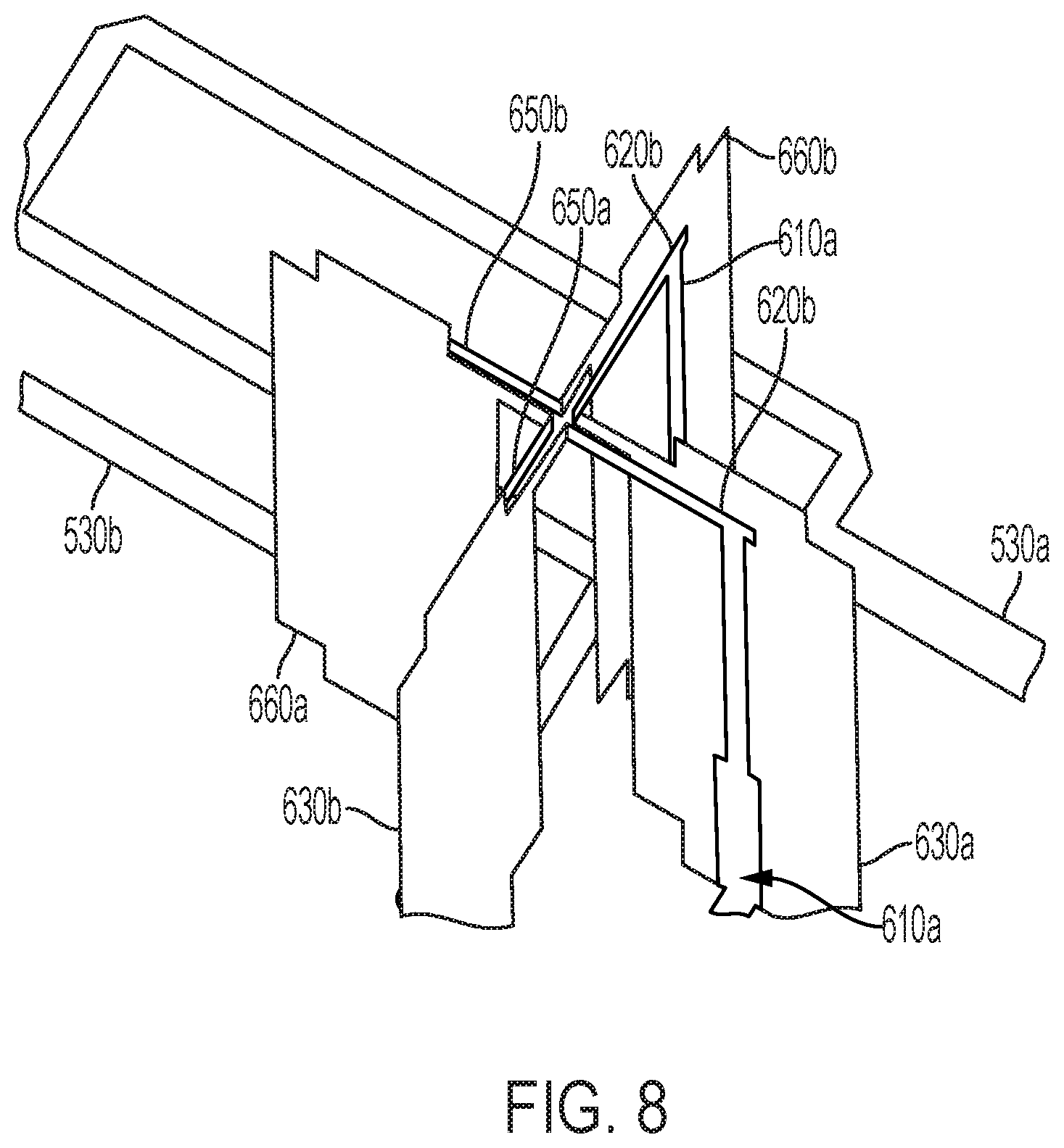
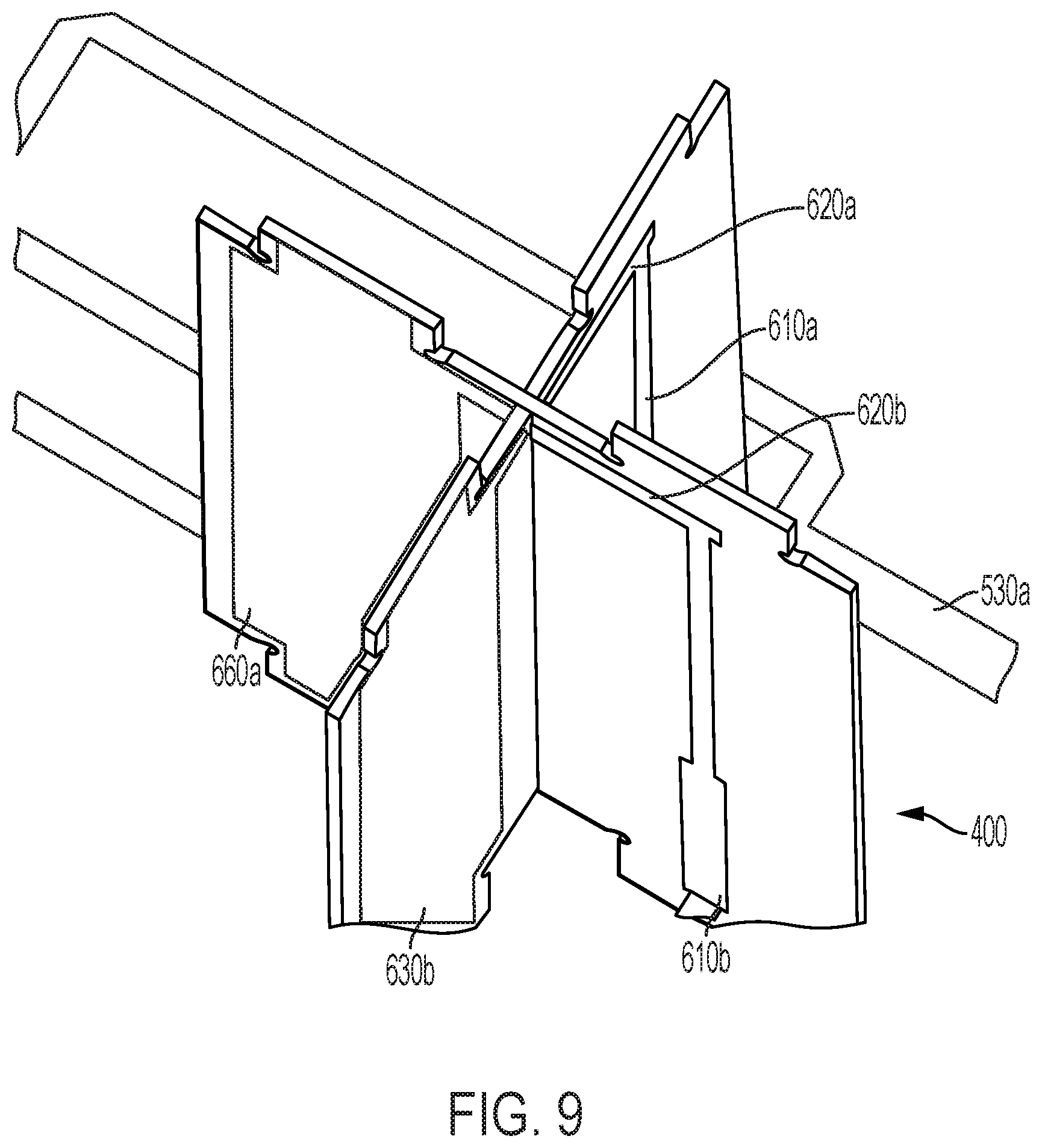
[0063] FIG. 8 provides a closer view of the combined drawings of FIGS. 7a and 7b, illustrating the respective connections between and relative orientations of microstrip baluns 620a/650a and microstrip ground plates 630a/660a (+45.degree.) and the respective connections between and relative orientations of microstrip baluns 620b/650b and microstrip ground plates 630b/660b (-45.degree.). FIG. 9 provides a similar view to that of FIG. 8, but with the stem plates present.
[0064] LB dipole 210 as described above may be operated in a circular polarization mode without modification to the components. To do this, instead of two separate RF signals being respectively assigned to the +45.degree. and -45.degree. signal paths, one may apply a single RF signal whereby, for example, the RF signal may be applied to +45.degree. signal feedline 510a, and the same RF signal, offset by a +90.degree. phase delay, may be applied to -45.degree. signal feedline 510b. In doing so, dipole arms 310a, 320b, 310b, 320a will radiate the same RF signal, each with a 90.degree. phase rotation between them, resulting in a left hand circular polarization RF propagation from LB dipole 210. Alternatively, applying an RF signal to the +45.degree. signal path, and the same RF signal with a -90.degree. phase delay, results in a right hand circular polarized propagation, in which dipole arms 310a, 320a, 310b, and 320b radiate the same RF signal, each with a 90.degree. phase rotation between them, generate a right hand circular RF propagation from LB dipole 210.
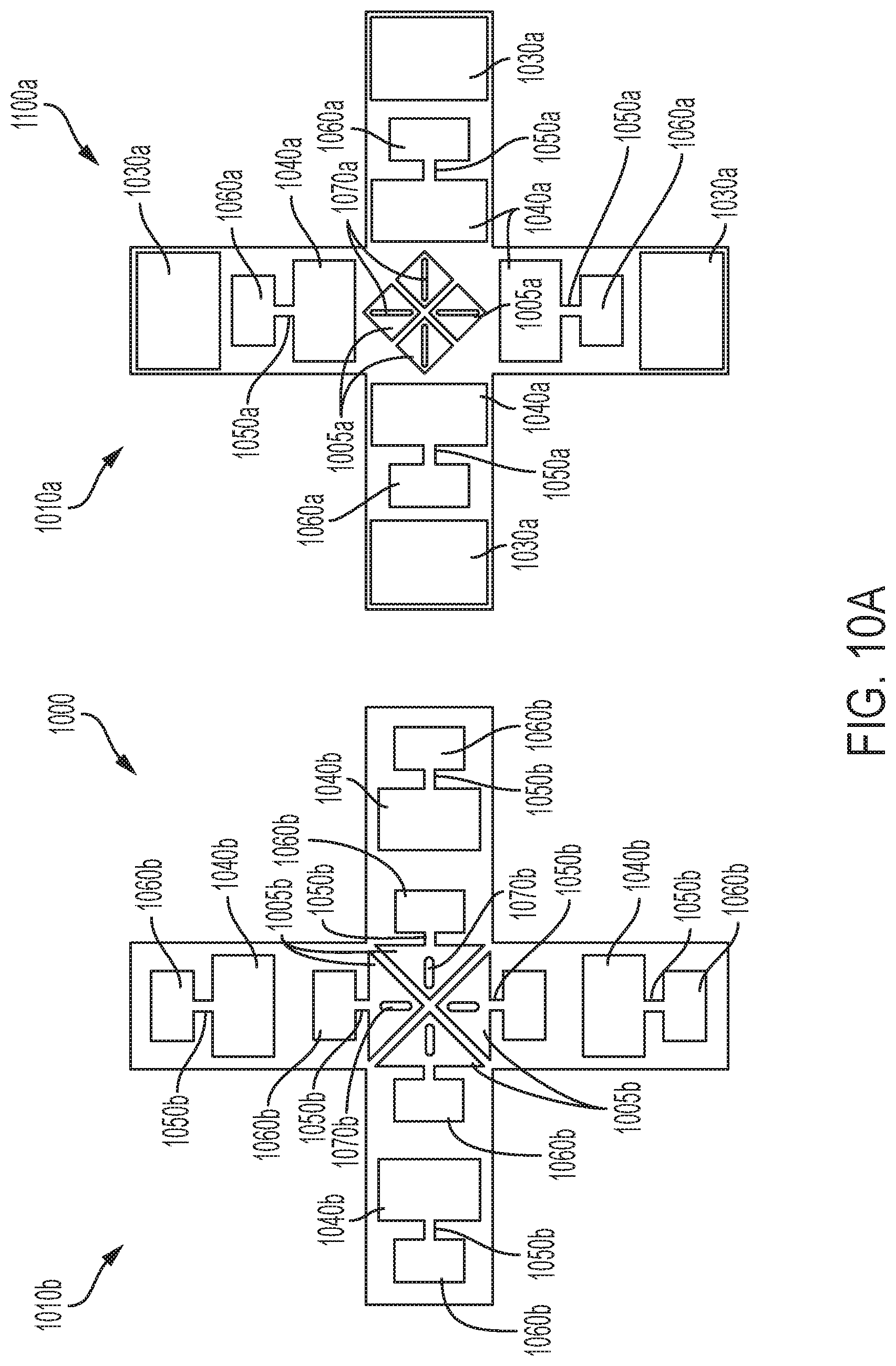
[0065] FIG. 10a illustrates an additional exemplary LB dipole 1000 according to the disclosure. LB dipole 1000 has a top side 1010a and a bottom side 1010b. Top side 1010a includes, at its center, four solder pads 1005a, each having a via 1070a through which a balun stem with a microstrip ground plate (not shown) are disposed so that the microstrip plate can be soldered to its respective solder pad 1005a. As illustrated, four dipole arms extend out from the center, on which are disposed a conductive element 1040a, an outward facing inductor trace 1050a that is coupled to a rectangular capacitive element 1060a. Further in the outward direction of each LB dipole arm is a distal conductive element 1030a, which may be substantially similar to conductive element 1040a.
[0066] Further illustrated in FIG. 10a is LB bottom side 1010b. Disposed in the center of LB bottom side 1010b are four arrowhead conductive elements 1005b, within which is disposed via 1070b through which a respective balun stem and microstrip plate (not shown) are disposed. Each arrowhead conductive element 1005b is coupled to an inductor trace 1050b, which is further coupled to a rectangular capacitive element 1060b. Disposed further outward on each LB dipole arm is a conductive element 1040b, each of which is coupled to an inductor trace 1050b and further coupled to a rectangular capacitive element 1060b.
[0067] FIG. 10b illustrates LB dipole 1000 along with a depiction of the inductors and capacitors that are formed by the elements on its top side 1010a and bottom side 1010b. As with the example illustrated in FIG. 4, the conductive elements 1040a/b and 1030a are each disposed opposite a rectangular conductive element 1060a/b whereby each LB dipole arm comprises a series of inductors and capacitors whereby the capacitors are formed by the LB dipole arm PCB substrate with the conductive elements and capacitive elements on opposite sides thereof. The series of inductors and capacitors are tuned such that the LB dipole 1000 radiate in the low band frequencies and are effectively short circuited at high band frequencies.
[0068] FIG. 11 illustrates another exemplary LB dipole 1100 according to the disclosure. An advantage of LB dipole 1100 is that its dipole arm span is shorter than LB dipole 1000, which reduces the interference or shadowing of the HB radiation patterns of HB dipoles 110. In order to preserve bandwidth, given the shorter arm span, each arm is wider than for LB dipole 1000. FIG. 11 provides exemplary dimensions of 177 mm for the length of a given dipole arm of LB dipole 1100, and 48.5 mm for the width. It will be understood that these dimensions are examples and that variations to these dimensions are possible and within the scope of the disclosure.
[0069] LB dipole 1100 has a top side 1110a and a bottom side 1110b. Top side 1110a has, at its center, four solder pads 1105a, each having a respective via 1170a through which a balun stem with a microstrip ground plate (not shown) are disposed so that the microstrip plate can be soldered to its respective solder pad 1105a. As illustrated, four dipole arms extend out from the center, on which are disposed a conductive element 1140a, an outward facing inductor trace 1150a that is coupled to a rectangular capacitive element 1160a. Further in the outward direction of each LB dipole arm is a distal conductive element 1130a, which may be substantially similar to conductive element 1140a. Top side 1110a also has a gap 1175a disposed between conductive elements 1140a. Gap 1175a may have a width of about 1 mm.
[0070] Further illustrated in FIG. 11 is LB bottom side 1110b. Disposed in the center of LB bottom side 1110b are four arrowhead conductive elements 1105b, within which is disposed via 1170b through which a respective balun stem and microstrip plate (not shown) are disposed. Each arrowhead conductive element 1105b has a portion of a "diamond" shaped capacitive element 1160b. Disposed further outward on each LB dipole arm is a conductive element 1140b, each of which is coupled to an inductor trace 1150b and further coupled to a diamond shaped capacitive element 1160b. The arrangement of a series of capacitors and inductors created by the structure of LB dipole 1100 is similar to that of LB dipole 1000 except for the partial diamond capacitive element 1160 on LB dipole 1100 and the gaps 1175a between adjacent conductive elements 1100a.
[0071] FIG. 12 plots the S-parameter performance of the exemplary LB dipole 1100.
[0072] It will be understood that either of LB dipole 1000 and LB dipole 1010 may be used with the balun and feed network described above, in place of LB dipole 210. This includes the circular polarization function described above and the 45 degree polarization tilting function described above with respect to FIG. 6c.
[0073] Further variations to the invention are possible and within the scope of the disclosure. For example, the disclosed structure of LB dipoles 210, 1000, and 1100 may be used Independently of the disclosed phase rotating feed network and balun circuitry. In such an example, the disclosed LB dipole 210/1000/1100 could be used with the antenna array face 100, in which case the feed network and balun circuitry may be of a conventional variety due to the fact that the radiated +/-45.degree. polarized RF propagation is parallel to each of the dipole arms. Further, other LB dipole structures may be used with the disclosed phase rotating feed network and balun circuitry. In this case, the substantial similarity between any alternative LB dipole and the disclosed LB dipoles include a cross-shaped arrangement of individual radiators, each of which is independently fed.
[0074] While various embodiments of the present invention have been described above, it should be understood that they have been presented by way of example only, and not limitation. It will be apparent to persons skilled in the relevant art that various changes in form and detail can be made therein without departing from the spirit and scope of the present invention. Thus, the breadth and scope of the present invention should not be limited by any of the above-described exemplary embodiments but should be defined only in accordance with the following claims and their equivalents.
* * * * *
D00000
D00001
D00002
D00003
D00004
D00005
D00006
D00007
D00008
D00009
D00010
D00011
D00012
D00013
D00014

D00015

D00016

XML
uspto.report is an independent third-party trademark research tool that is not affiliated, endorsed, or sponsored by the United States Patent and Trademark Office (USPTO) or any other governmental organization. The information provided by uspto.report is based on publicly available data at the time of writing and is intended for informational purposes only.
While we strive to provide accurate and up-to-date information, we do not guarantee the accuracy, completeness, reliability, or suitability of the information displayed on this site. The use of this site is at your own risk. Any reliance you place on such information is therefore strictly at your own risk.
All official trademark data, including owner information, should be verified by visiting the official USPTO website at www.uspto.gov. This site is not intended to replace professional legal advice and should not be used as a substitute for consulting with a legal professional who is knowledgeable about trademark law.