Method For Manufacturing A Semiconductor Device
Kang; HeeSung ; et al.
U.S. patent application number 16/828885 was filed with the patent office on 2020-10-01 for method for manufacturing a semiconductor device. The applicant listed for this patent is ASM IP Holding B.V.. Invention is credited to HeeSung Kang, YoungHoon Kim, JaeOk Ko, WanGyu Lim, YoonKi Min, JinGeun Yu.
| Application Number | 20200312652 16/828885 |
| Document ID | / |
| Family ID | 1000004746295 |
| Filed Date | 2020-10-01 |


View All Diagrams
| United States Patent Application | 20200312652 |
| Kind Code | A1 |
| Kang; HeeSung ; et al. | October 1, 2020 |
METHOD FOR MANUFACTURING A SEMICONDUCTOR DEVICE
Abstract
A substrate processing method with an improved etch selectivity includes: a first operation for forming a film on a stepped structure having a top surface, a bottom surface, and a side surface connecting the top surface and the bottom surface, wherein a first atmosphere is set to reduce a mean free path of plasma ions and to cause the plasma ions to have no directionality; and a second operation for changing a bonding structure of a portion of the film, wherein a second atmosphere is set to cause the plasma ions to have directionality, wherein the first operation is repeated a plurality of times, the second operation is performed for a predetermined time period, the first operation and the second operation form a group cycle, and the group cycle is repeated by a plurality of times.
| Inventors: | Kang; HeeSung; (Osan-si, KR) ; Min; YoonKi; (Dongjak-gu, KR) ; Lim; WanGyu; (Icheon-si, KR) ; Yu; JinGeun; (Cheonan-si, KR) ; Ko; JaeOk; (Gangseo-gu, KR) ; Kim; YoungHoon; (Cheonan-si, KR) | ||||||||||
| Applicant: |
|
||||||||||
|---|---|---|---|---|---|---|---|---|---|---|---|
| Family ID: | 1000004746295 | ||||||||||
| Appl. No.: | 16/828885 | ||||||||||
| Filed: | March 24, 2020 |
Related U.S. Patent Documents
| Application Number | Filing Date | Patent Number | ||
|---|---|---|---|---|
| 62827713 | Apr 1, 2019 | |||
| Current U.S. Class: | 1/1 |
| Current CPC Class: | H01L 21/31111 20130101; H01L 21/0217 20130101; H01L 21/0228 20130101; H01L 21/0234 20130101 |
| International Class: | H01L 21/02 20060101 H01L021/02; H01L 21/311 20060101 H01L021/311 |
Claims
1. A substrate processing method comprising: a first operation for forming a film on a stepped structure having a top surface, a bottom surface, and a side surface connecting the top surface and the bottom surface, wherein a first atmosphere is set to reduce a mean free path of plasma ions and to cause the plasma ions to have no directionality; and a second operation for changing a bonding structure of a portion of the film, wherein a second atmosphere is set to cause the plasma ions to have directionality; wherein the first operation is repeated a plurality of times, the second operation is performed for a predetermined time period, the first operation and the second operation form a group cycle, and the group cycle is repeated by a plurality of times.
2. The substrate processing method of claim 1, further comprising performing isotropic etching on the film formed by performing the group cycle a plurality of times.
3. The substrate processing method of claim 2, wherein, during the isotropic etching, an etch selectivity between the portion of the film whose bonding structure has changed and the other remaining portion of the film is achieved.
4. The substrate processing method of claim 2, wherein, in a group cycle, the first operation is performed m times, the second operation is performed for n seconds, and a ratio of n to m is adjusted to control a profile of a remaining film through the isotropic etching.
5. The substrate processing method of claim 2, wherein, during the second operation, the bonding structure of the portion of the film is weakened by an ion bombardment effect of the plasma ions.
6. The substrate processing method of claim 5, wherein the plasma ions have directionality that is perpendicular to the top surface and the bottom surface of the stepped structure, so that after the isotropic etching, a portion of the film formed on the top and bottom surfaces of the stepped structure is removed and a portion of the film formed on the side surface of the stepped structure remains.
7. The substrate processing method of claim 1, wherein pressure in the first atmosphere is higher than pressure in the second atmosphere.
8. The substrate processing method of claim 1, wherein plasma power in the first atmosphere is lower than plasma power in the second atmosphere.
9. The substrate processing method of claim 1, wherein a temperature in the first atmosphere is higher than a temperature in the second atmosphere.
10. The substrate processing method of claim 1, wherein the first operation comprises: supplying a first gas; purging the first gas; and supplying a second gas and performing first plasma treatment to form the film.
11. The substrate processing method of claim 10, wherein the second operation comprises performing second plasma treatment on the film.
12. A substrate processing method comprising: supplying a first source gas; purging the first source gas; supplying a first reaction gas and performing first plasma treatment to form a first film; supplying a second source gas onto the first film; purging the second source gas; supplying a second reaction gas and performing second plasma treatment to form a second film on the first film; and performing third plasma treatment on at least a portion of the first film and the second film, wherein the first film and the second film comprise the same material.
13. The substrate processing method of claim 12, further comprising: supplying a third source gas onto the second film; supplying a third reaction gas and performing fourth plasma treatment to form a third film on the second film; and performing fifth plasma treatment on the third film, wherein the first film, the second film, and the third film comprise the same material.
14. The substrate processing method of claim 13, wherein the film is formed on a stepped structure having a top surface, a bottom surface, and a side surface connecting the top surface and the bottom surface, and a bonding structure of a portion of the film formed on the top and bottom surfaces of the stepped structure is weakened by the third plasma treatment and the fifth plasma treatment.
15. The substrate processing method of claim 13, wherein the first plasma treatment, the second plasma treatment, and the fourth plasma treatment are performed under first pressure, and the third plasma treatment and the fifth plasma treatment are performed under second pressure that is lower than the first pressure.
16. The substrate processing method of claim 13, wherein, during the first plasma treatment, the second plasma treatment, and the fourth plasma treatment, first power is supplied, and during the third plasma treatment and the fifth plasma treatment, second power that is higher than the first power is supplied.
17. A substrate processing method comprising: performing a group cycle a plurality of times, wherein the group cycle comprises: a first operation for performing first plasma treatment to form a film on a stepped structure having a top surface, a bottom surface, and a side surface connecting the top surface and the bottom surface; and a second operation for performing second plasma treatment on the film, wherein, during a group cycle, the first operation is performed a plurality of times.
18. The substrate processing method of claim 17, wherein, during the first plasma treatment, pressure of a reaction space is maintained at a first pressure, and during the second plasma treatment, pressure of the reaction space is maintained at a second pressure that is lower than the first pressure.
19. The substrate processing method of claim 17, wherein a power that is supplied during the first plasma treatment is lower than a power that is supplied during the second plasma treatment.
20. The substrate processing method of claim 17, further comprising, after the group cycle is performed a plurality of times, performing isotropic etching to remove a portion of the film on the stepped structure to expose a surface of the stepped structure.
Description
CROSS-REFERENCE TO RELATED APPLICATION
[0001] This application claims the benefit of U.S. Provisional Application No. 62/827,713, filed on Apr. 1, 2019, in the United States Patent and Trademark Office, the disclosure of which is incorporated herein in its entirety by reference.
BACKGROUND
1. Field
[0002] One or more embodiments relate to a method of manufacturing a semiconductor device, and more particularly, to a method of manufacturing a semiconductor device, which is capable of improving an etch selectivity of a film formed on a stepped structure.
2. Description of the Related Art
[0003] In a process for manufacturing a device in which a microcircuit is formed on a substrate, a technique for forming a thin film on a structure having steps is used. Particularly, high density integrated circuits such as a three-dimensional semiconductor device include a trench structure or a stepped structure, and a thin film needs to be formed on a selected area of the structure.
SUMMARY
[0004] The present disclosure provides a substrate processing method of forming a deposition film having a high etch selectivity on a stepped structure having a high aspect ratio to pattern the film by an isotropic etch process without performing a lithography process.
[0005] The present disclosure provides a substrate processing method capable of controlling a profile of a deposition film formed on a stepped structure.
[0006] Additional aspects will be set forth in part in the description which follows and, in part, will be apparent from the description, or may be learned by practice of the presented embodiments.
[0007] According to an aspect of embodiments based on a technical concept of the disclosure, a substrate processing method includes: a first operation for forming a film on a stepped structure having a top surface, a bottom surface, and a side surface connecting the top surface and the bottom surface, wherein a first atmosphere is set to reduce a mean free path of plasma ions and to cause the plasma ions to have no directionality; and a second operation for changing a bonding structure of a portion of the film, wherein a second atmosphere is set to cause the plasma ions to have directionality, wherein the first operation is repeated a plurality of times, the second operation is performed for a predetermined time period, the first operation and the second operation form a group cycle, and the group cycle is repeated by a plurality of times.
[0008] According to an example of the substrate processing method, the substrate processing method may further include performing isotropic etching on a film formed by performing the group cycle a plurality of times.
[0009] According to another example of the substrate processing method, during the isotropic etching, an etch selectivity between the portion of the deposition film whose bonding structure has changed and the other portion of the deposition film may be achieved.
[0010] According to another example of the substrate processing method, in a group cycle, the first operation may be performed m times, the second operation may be performed for n seconds, and a ratio of n to m may be adjusted to control a profile of a remaining film through the isotropic etching.
[0011] According to another example of the substrate processing method, during the second operation, the bonding structure of the portion of the film may be weakened by an ion bombardment effect of the plasma ions.
[0012] According to another example of the substrate processing method, the plasma ions may have directionality that is perpendicular to the top surface and the bottom surface of the stepped structure, so that after the isotropic etching, a portion of the film formed on the top and bottom surfaces is removed and a portion of the film on the side surface remains.
[0013] According to another example of the substrate processing method, pressure in the first atmosphere may be higher than pressure in the second atmosphere.
[0014] According to another example of the substrate processing method, plasma power in the first atmosphere may be lower than plasma power in the second atmosphere.
[0015] According to another example of the substrate processing method, a temperature in the first atmosphere may be higher than a temperature in the second atmosphere.
[0016] According to another example of the substrate processing method, the first operation may include: supplying a first gas; purging the first gas; and supplying a second gas and performing first plasma treatment to form the film.
[0017] According to another example of the substrate processing method, the second operation may include performing second plasma treatment on the film.
[0018] According to another aspect of embodiments based on a technical concept of the disclosure, a substrate processing method includes: supplying a first source gas; purging the first source gas; supplying a first reaction gas and performing first plasma treatment to form a first film; supplying a second source gas onto the first film; purging the second source gas; supplying a second reaction gas and performing second plasma treatment to form a second film on the first film; and performing third plasma treatment on at least a portion of the first film and the second film, wherein the first film and the second film form a film including the same material.
[0019] According to an example of the substrate processing method, the substrate processing method may further include: supplying a third source gas onto the second deposition film; supplying a third reaction gas and performing fourth plasma treatment to form a third film on the second film; and performing fifth plasma treatment on the third film, wherein the first film, the second film, and the third film form a film including the same material.
[0020] According to another example of the substrate processing method, the film may be formed on a stepped structure having a top surface, a bottom surface, and a side surface connecting the top surface and the bottom surface, and a bonding structure of a portion of the film formed on the top and bottom surfaces may be weakened by the third plasma treatment and the fifth plasma treatment.
[0021] According to another example of the substrate processing method, the first plasma treatment, the second plasma treatment, and the fourth plasma treatment may be performed under first pressure, and the third plasma treatment and the fifth plasma treatment may be performed under second pressure that is lower than the first pressure.
[0022] According to another example of the substrate processing method, during the first plasma treatment, the second plasma treatment, and the fourth plasma treatment, a first power may be supplied, and during the third plasma treatment and the fifth plasma treatment, a second power than is higher than the first power may be supplied.
[0023] According to another aspect of embodiments based on a technical concept of the disclosure, a substrate processing method includes: performing a group cycle a plurality of times, wherein the group cycle comprises: a first operation for performing first plasma treatment to form a film on a stepped structure having a top surface, a bottom surface, and a side surface connecting the top surface and the bottom surface; and a second operation for performing second plasma treatment on the film, wherein during a group cycle, the first operation is performed a plurality of times.
[0024] According to an example of the substrate processing method, during the first plasma treatment, pressure of a reaction space may be maintained at first pressure, and during the second plasma treatment, pressure of the reaction space may be maintained at a second pressure that is lower than the first pressure.
[0025] According to another example of the substrate processing method, power that is supplied during the first plasma treatment may be lower than power that is supplied during the second plasma treatment.
[0026] According to another example of the substrate processing method, the substrate processing method may further include, after the group cycle is performed a plurality of times, performing isotropic etching to remove a portion of the film on the stepped structure to expose a surface of the stepped structure.
BRIEF DESCRIPTION OF THE DRAWINGS
[0027] These and/or other aspects will become apparent and more readily appreciated from the following description of the embodiments, taken in conjunction with the accompanying drawings in which:
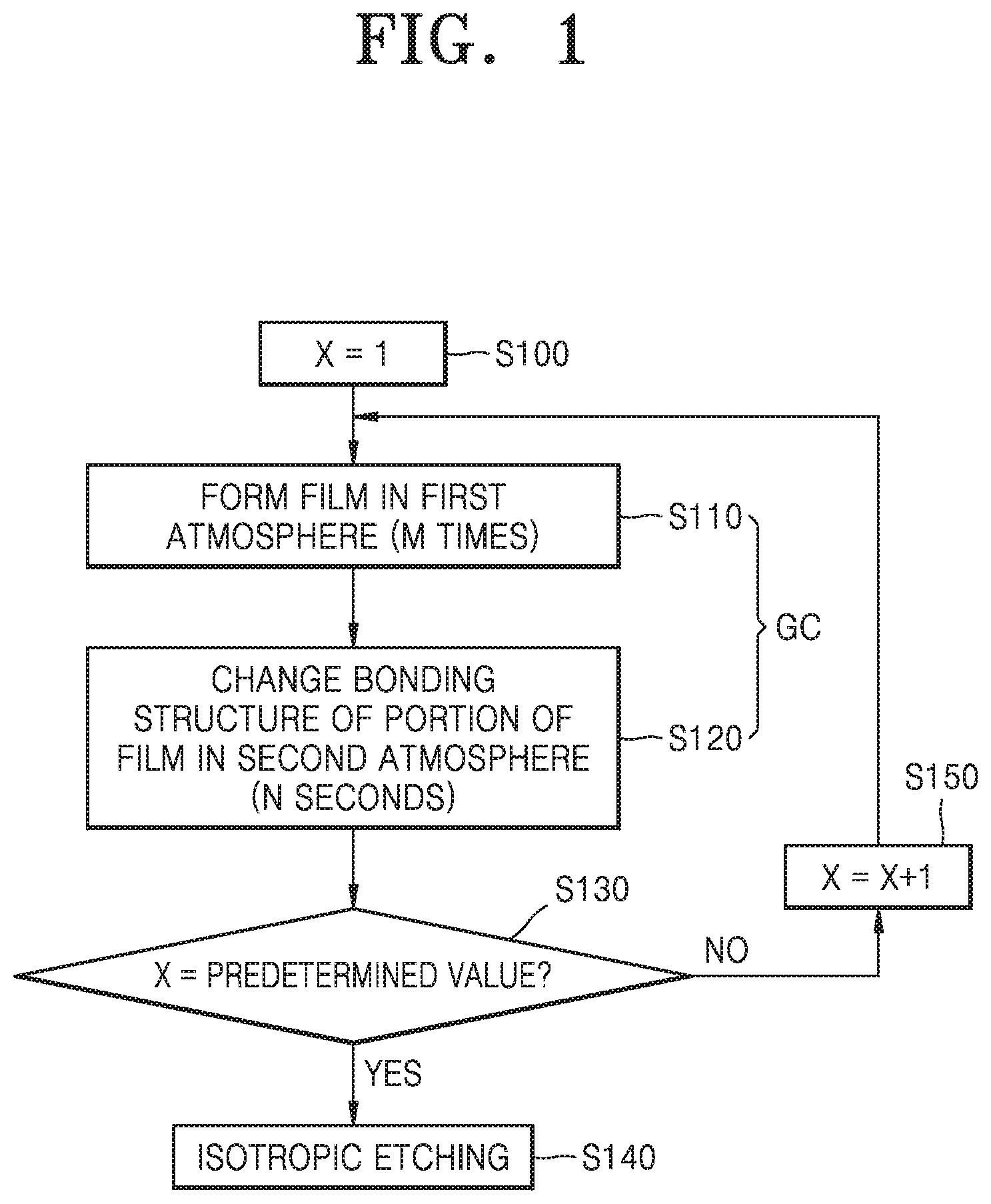
[0028] FIG. 1 is a flowchart schematically showing a substrate processing method according to embodiments based on a technical concept of the disclosure;
[0029] FIGS. 2 and 3 schematically show substrate processing methods according to embodiments based on a technical concept of the disclosure;
[0030] FIG. 4 schematically shows a substrate processing method according to embodiments based on a technical concept of the disclosure;
[0031] FIG. 5 schematically shows a substrate processing method according to embodiments based on a technical concept of the disclosure;
[0032] FIG. 6 shows features that may occur in the substrate processing method of FIG. 5;
[0033] FIGS. 7 and 8 schematically show substrate processing methods according to embodiments based on a technical concept of the disclosure;
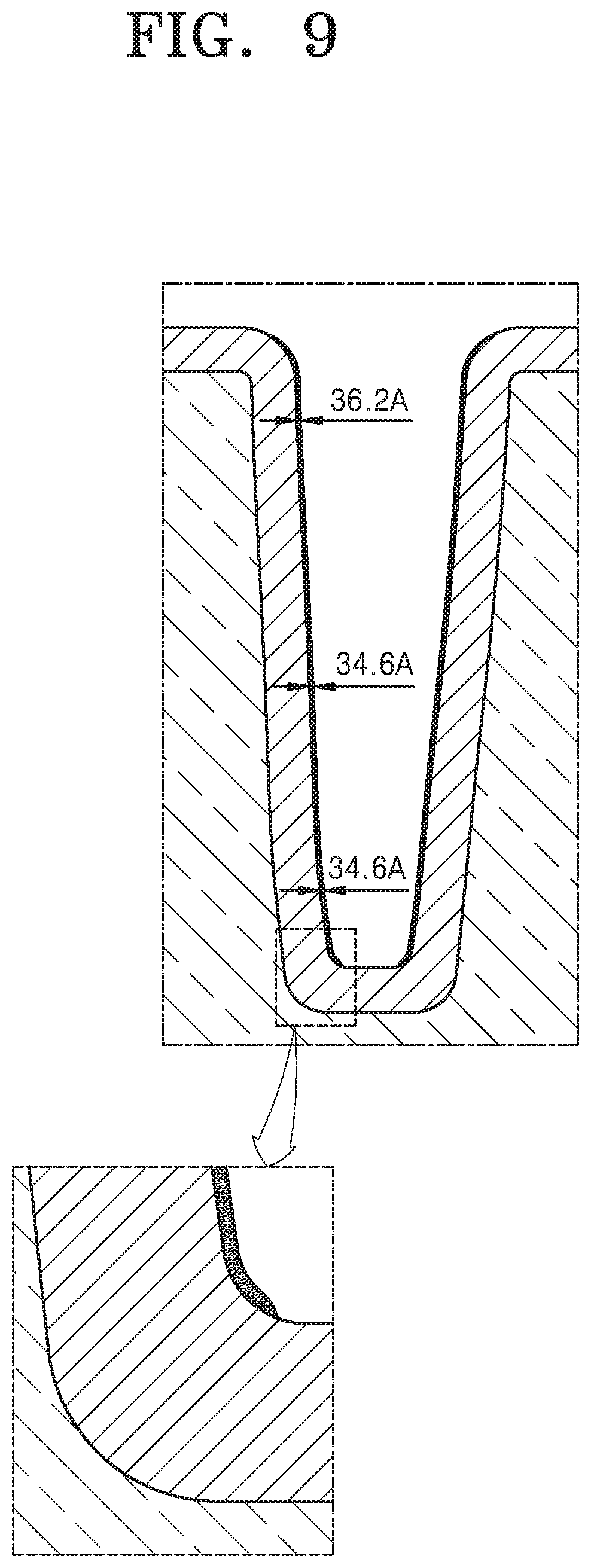
[0034] FIG. 9 shows a state after the substrate processing method according to the embodiments of FIGS. 7 and 8 is performed;
[0035] FIG. 10 shows states after thin films are deposited and wet etching is performed according to various conditions;
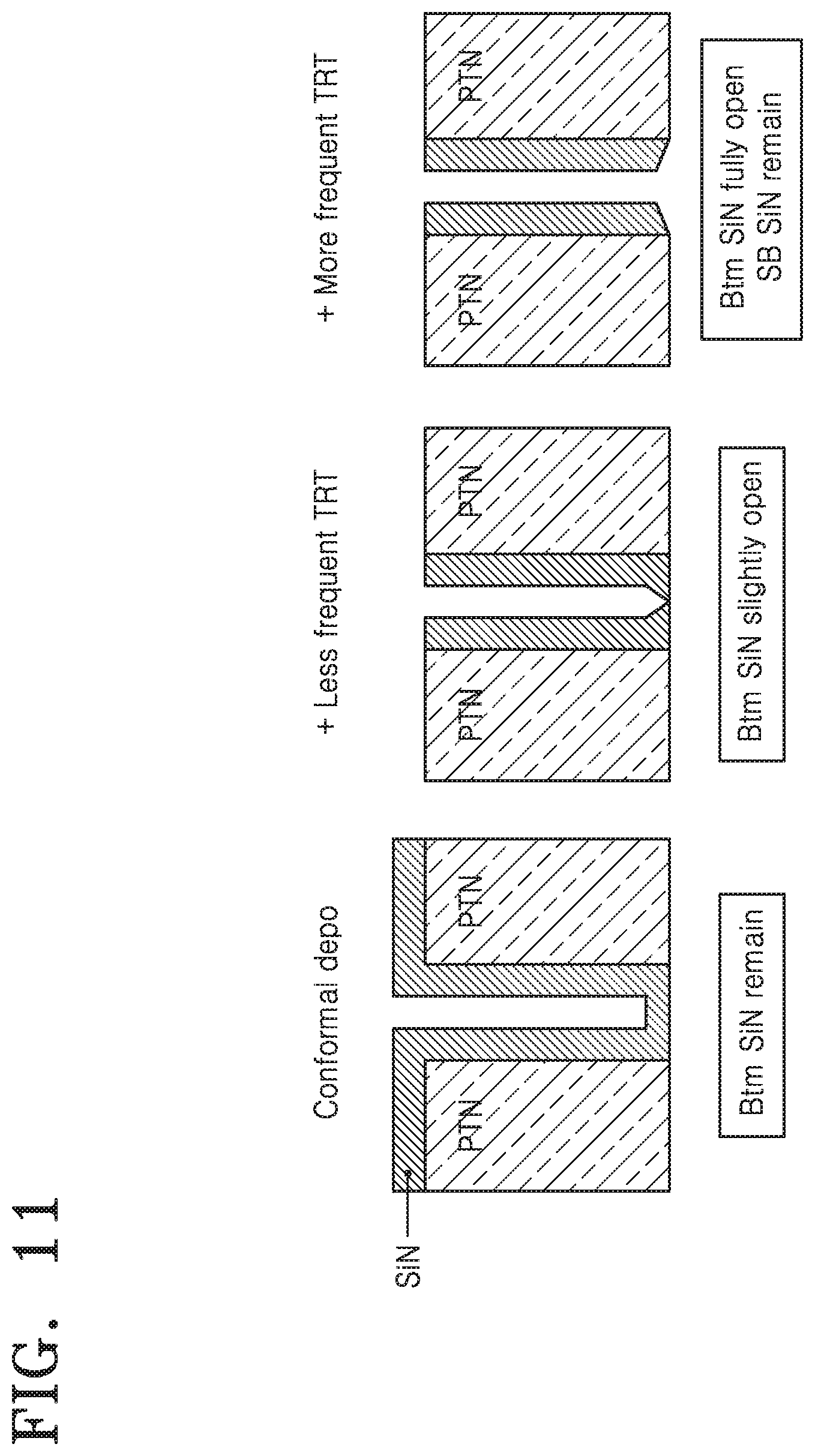
[0036] FIG. 11 shows a state in which a profile of a thin film structure is controlled by changing conditions; and
[0037] FIG. 12 schematically shows a substrate processing method according to embodiments based on a technical concept of the disclosure.
DETAILED DESCRIPTION
[0038] Reference will now be made in detail to embodiments, examples of which are illustrated in the accompanying drawings, wherein like reference numerals refer to like elements throughout. In this regard, the present embodiments may have different forms and should not be construed as being limited to the descriptions set forth herein. Accordingly, the embodiments are merely described below, by referring to the figures, to explain aspects of the present description. As used herein, the term "and/or" includes any and all combinations of one or more of the associated listed items. Expressions such as "at least one of," when preceding a list of elements, modify the entire list of elements and do not modify the individual elements of the list.
[0039] Hereinafter, embodiments of the disclosure will be described with reference to the accompanying drawings.
[0040] The embodiments of the disclosure are provided to allow those having ordinary skill in the art to completely understand the disclosure. The embodiments may, however, be embodied in many different forms, and the scope of the disclosure should not be construed as being limited to the embodiments set forth herein. Rather, these embodiments are provided so that the disclosure will be thorough and complete, and will fully convey the concept of the disclosure to one of ordinary skill in the art.
[0041] The terminology used herein is for the purpose of describing particular embodiments only and is not intended to be limiting of the disclosure. As used herein, the singular forms "a," "an" and "the" are intended to include the plural forms as well, unless the context clearly indicates otherwise. It will be further understood that the terms "comprises" and/or "comprising," when used in this specification, specify the presence of stated features, integers, steps, operations, elements, components, and/or groups thereof, but do not preclude the presence or addition of one or more other features, integers, steps, operations, elements, components, and/or groups thereof. As used herein, the term "and/or" includes any and all combinations of one or more of the associated listed items.
[0042] It will be understood that although the terms "first," "second," etc. may be used herein to describe various members, areas, layers, portions, and/or components, these members, areas, layers, portions, and/or components should not be limited by these terms. These components do not indicate a specific order or superiority, but are only used to distinguish one member, area, layer, portion or component from another. Therefore, first members, areas, portions, or components may indicate second members, areas, portions, or components without departing from teachings of the present disclosure.
[0043] In the present specification, the term "gas" may include an evaporated solid and/or liquid, and may be a single gas or a mixture of gases. In the present specification, a process gas introduced into a reaction chamber via a shower head may include a precursor gas and an additive gas. The precursor gas and the additive gas may be typically introduced into a reaction space in the form of a mixed gas or may be independently introduced into the reaction space. The precursor gas may be introduced together with a carrier gas, such as an inert gas. The additive gas may include a reactant gas and a dilute gas, such as an inert gas. The reactant gas and the dilute gas may be mixed and introduced into the reaction space, or may be independently introduced into the reaction space. A precursor may include two or more precursors, and a reactant gas may include two or more reactant gases. The precursor is a gas chemisorbed onto a substrate and typically containing metalloid or metal atoms that form a major structure of a matrix of a dielectric film, and the reactant gas for deposition is a gas that reacts with the precursor chemisorbed onto the substrate when the gas is excited to form an atomic layer or a monolayer onto the substrate. "Chemisorption" refers to chemically-saturated adsorption. A gas other than the process gas, namely, a gas introduced, other than via the shower head, may be used to seal the reaction space. The gas includes a seal gas, such as an inert gas. According to some embodiments, a "film" refers to a layer that continuously extends in a direction perpendicular to a thickness direction without pin holes in order to cover the entire area of a target or a partial surface related to the target, or a layer that simply covers the target or the partial surface related with the target. According to some embodiments, a "layer" refers to a structure having a certain thickness formed on a surface, a film-type layer, or a non-film structure. A film or layer may be a single discontinuous film or layer having certain characteristics or may include multiple films or layers. A boundary between adjacent films or layers may be clear or unclear and may be set based on physical characteristics, chemical characteristics, and/or other types of characteristics, forming processes or a forming sequence, and/or functions or purposes of adjacent films or layers.
[0044] In the present specification, a phrase "containing a Si--N bond" may be characterized by a Si--N bond or Si--N bonds which may have a main frame substantially formed by a Si--N bond or Si--N bonds and/or a substituent substantially formed by a Si--N bond or Si--N bonds. A silicon nitride layer may be a dielectric layer containing a Si--N bond and may include a silicon nitride layer (SiN) and a silicon oxynitride layer (SiON).
[0045] In the present specification, the term "the same material" should be interpreted as including the same main constituent. For example, when a first layer and a second layer are both silicon nitride layers and are formed of the same material, the first layer may be selected from the group consisting of Si.sub.2N, SiN, Si.sub.3N.sub.4, and Si.sub.2N.sub.3 and the second layer may also be selected from the same group, but in detail, a film material of the second layer may be different from that of the first layer.
[0046] In addition, in the present specification, an executable range may be determined based on a routine operation, two parameters may constitute an executable range, and an indicated range may include or exclude end points. In addition, values of some indicated parameters (regardless of whether or not the values are indicated by "about") may refer to accurate values or approximate values, and may include equivalents thereof. According to some embodiments, the values of some indicated parameters may refer to an average value, a center value, a representative value, a multi value, and the like.
[0047] In the present specification, when conditions and/or structures are not specified, one of ordinary skill in the art may easily provide these conditions and/or structures as an issue of a customary experiment. In all disclosed embodiments, a component used in one embodiment includes components disclosed explicitly, necessarily, or intrinsically herein for intended purposes, and thus may be replaced by any of components equivalent to the component. Furthermore, the present disclosure is equally applicable to devices and methods.
[0048] Hereinafter, embodiments according to a technical concept of the disclosure will be described with reference to the drawings. In the drawings, variations from the shapes of the illustrations as a result, for example, of manufacturing techniques and/or tolerances, are to be expected. Thus, the embodiments of the disclosure should not be construed as being limited to the particular shapes of regions illustrated herein but are to include deviations in shapes that result, for example, from manufacturing.
[0049] FIG. 1 is a flowchart schematically showing a substrate processing method according to embodiments based on a technical concept of the disclosure.
[0050] Referring to FIG. 1, a film may be formed in a first atmosphere, in a first operation S110. The film may be formed on a stepped structure. That is, the film may be formed on a stepped structure having a top surface, a bottom surface, and a side surface connecting the top surface and the bottom surface. The stepped structure may be a structure with a high aspect ratio, and the aspect ratio may be, for example, width:height=1:10 or more. To form a conformal deposition film on the stepped structure having the high aspect ratio, an atomic layer deposition (ALD) process may be used. More specifically, a plasma atomic layer deposition (PEALD) process may be used.
[0051] The first atmosphere in which the deposition film is formed may be set such that a mean free path of plasma ions is reduced and the plasma ions have no directionality (that is, such that random movements of the plasma ions increase). The first atmosphere may contribute to forming the conformal deposition film on the stepped structure having the high aspect ratio. To achieve the first atmosphere, a high-pressure (for example, 10 Torr to 20 Torr) atmosphere may be created. According to another embodiment, to achieve the first atmosphere, a low-power atmosphere (for example, 200 W to 500 W) may be created. According to still another embodiment, to achieve the first atmosphere, a high-temperature atmosphere may be created.
[0052] The first operation S110 of forming the film on the stepped structure may include an operation of performing first plasma treatment. More specifically, the first operation S110 may include an operation of supplying a first gas, an operation of purging the first gas, an operation of supplying a second gas, an operation of performing first plasma treatment, and an operation of purging the second gas. While the first plasma treatment is performed, the second gas may be excited, and the second gas having reactivity may react with the first gas to form the film.
[0053] The first gas, which is a source gas, may include a material that is chemisorbed on a substrate. The second gas may include a material having reactivity with the first gas, particularly, a material having reactivity with the first gas under a plasma atmosphere. According to a selective embodiment, the operation of supplying the second gas and the operation of performing the first plasma treatment may be performed simultaneously.
[0054] The operation (that is, the first operation S110) of forming the film on the stepped structure under the first atmosphere may be performed a plurality of times (for example, M times). More specifically, a group cycle GC may be performed a plurality of times to deposit a film, and during each group cycle GC, the first operation S110 may be performed a plurality of times. The number of repetitions of the first operation S110 relates to a second atmosphere that is set in a subsequent second operation S120. In other words, the first operation S110 may be performed repeatedly by a predetermined number of times (that is, M times) to form a film of a thickness that is suitable for plasma treatment which will be performed in the second atmosphere.
[0055] After the first operation S110 is performed a plurality of times, the second operation S120 of changing a bonding structure of a portion of the film may be performed. During the second operation S120, second plasma treatment may be performed on the film to change a bonding structure of a portion of the film. It is noted that the second plasma treatment during the second operation S120 is different from the first plasma treatment that has been performed during the first operation S110. The second operation S120 may be performed in the second atmosphere, and the second atmosphere may be set such that plasma ions have directionality. In contrast, the first operation S110 may be performed in the first atmosphere, and the first atmosphere may be set such that plasma ions have no directionality.
[0056] The plasma ions having directionality, which are supplied during the second operation S120, may change a bonding structure of a portion of the film. For example, when a film is formed on a stepped structure having an aspect ratio, the directionality of plasma ions may be set to be toward a top surface or a bottom surface of the stepped structure. In this case, the plasma ions may change the bonding structure of the film formed on the top surface or the bottom surface of the stepped structure. In contrast, the plasma ions with the directionality may have little influence on the bonding structure of the film formed on the side surface of the stepped structure.
[0057] The change of the bonding structure of the portion of the film, caused by the plasma ions, may be weakening (see FIG. 2) of the bonding structure or densification (see FIG. 3) of the bonding structure. Hereinafter, embodiments of the disclosure will be described in more detail assuming weakening of the bonding structure.
[0058] During the second operation S120, the bonding structure of the portion of film may be weakened by an ion bombardment effect of the plasma ions. More specifically, the plasma ions may have directionality that is perpendicular to the top surface and the bottom surface of the stepped structure. Accordingly, the bonding structure of the top surface and the bottom surface of the film may be weakened. As a result, in a subsequent isotropic etching operation S140, the film formed on the top and bottom surfaces of the stepped structure may be removed, and the film formed on the side surface of the stepped structure may remain.
[0059] During the second operation S120, a gas of the same material as the second gas (for example, a reaction gas) supplied in the first operation S110 may be supplied. A gas supply condition in the second operation S120 may be different from that in the first operation S110. For example, nitrogen may be supplied as a reaction gas during the first operation S110 and the second operation S120. In this case, the amount of a nitrogen gas supplied in the second operation S120 may be less than that supplied in the first operation S110. Also, the temperature of the nitrogen gas supplied in the second operation S120 may be lower than that supplied in the first operation S110. Also, plasma power applied to the nitrogen gas supplied in the second operation S120 may be lower than that supplied in the first operation S110.
[0060] Under this supply conditions, as described above, in the first operation S110, random movements of the reaction gas (for example, a nitrogen gas) may increase to form a film of uniform quality in both horizontal and vertical directions, whereas in the second operation S120, the directionality of the reaction gas (for example, a nitrogen gas) may increase to change a bonding structure of the film (that is, the film formed on the top and bottom surfaces of the stepped structure) in the vertical direction.
[0061] To increase the random movements of the reaction gas in the first operation S110, pressure of the reaction space may be maintained at a first pressure (for example, high pressure) during the first plasma treatment. In contrast, to cause the movements of the reaction gas to have directionality in the second operation S120, pressure of the reaction space may be maintained at a second pressure (for example, low pressure) that is lower than the first pressure, during the second plasma treatment.
[0062] Also, to cause the reaction gas to be less influenced by power (that is, to cause the plasma ions to have no directionality) in the first operation S110, power that is supplied during the first plasma treatment may be maintained at a first power value (for example, a low power value). In contrast, to cause the reaction gas to be more influenced by power (that is, to cause the plasma ions to have directionality) in the second operation S120, power that is supplied during the second plasma treatment may be maintained at a second power value (for example, a high power value) that is higher than the first power value.
[0063] In some alternative embodiments, to change the bonding structure of the deposition film during the second operation S120, a gas (for example, a hydrogen-containing nitrogen gas) including hydrogen may be supplied into the reaction space. By performing plasma treatment by using the gas including hydrogen, more Si--H bonds may be formed in the film formed on the top and bottom surfaces of the stepped structure, and therefore, a wet etch rate (WER) may increase at the corresponding portions of the film during a subsequent etching processing.
[0064] The first operation S110 that is performed a plurality of times in the first atmosphere and the second operation S120 that is performed for a predetermined time period (for example, N seconds) in the second atmosphere may be defined as a group cycle GC, and the group cycle GC may be performed repeatedly. In other words, before a group cycle GC is performed, an X value may be set to 1 in operation S100, and when a group cycle GC including the first operation S110 and the second operation S120 is performed, the X value may increase in operation S150. When the X value reaches a predetermined value in operation S130, the group cycle GC may terminate and the subsequent isotropic etching operation S140 may be performed.
[0065] Thereafter, the isotropic etching operation S140 may be performed on a film formed by performing the group cycle GC a plurality of times. For example, wet etching may be performed on the film. For example, wet etching of dipping a semiconductor device, that is, a substrate with a thin film thereon, into a liquid etching solution to etch the surface of the substrate by a chemical reaction may be performed. Because the wet etching is isotropic etching, the isotropic etching may not greatly affect selective etching of the film formed on the stepped structure.
[0066] During the isotropic etching operation S140, an etch selectivity between the portions of the film whose bonding structure has changed and the other portions of the film may be achieved. In other words, by performing the second operation S120 of applying plasma to the film after the first operation S110 of forming the film on the stepped structure, a bonding structure of some portions of the film on the stepped structure may change, and accordingly, during isotropic etching, some portions of the film may be removed and the other portions of the film may remain. Because some portions of the film on the stepped structure are removed, the corresponding surface of the stepped structure may be exposed. Accordingly, selective etching of the deposition film may be achieved by a subsequent etching process. Therefore, a patterned film may be formed on an area of the stepped structure without performing an additional photolithography process.
[0067] According to an alternative embodiment, in a group cycle GC, the first operation S110 may be performed M times, the second operation S120 may be performed for N seconds, and a ratio of M and N may be adjusted to control a profile of the remaining deposition film by isotropic etching. For example, by increasing an N value with respect to an M value, an etch selectivity between the film formed on the top and bottom surfaces of the stepped structure and the film formed on the side surface of the stepped structure may increase. By adjusting the etch selectivity, a degree by which the bottom surface of the stepped structure is exposed may be adjusted (see FIG. 10). That is, by adjusting the M value and the N value, a profile of the deposition film remaining on the bottom surface of the stepped structure may be finely adjusted.
[0068] As such, according to the embodiments based on the technical concept of the disclosure, instead of performing a first operation of forming a film with a thickness of a nanometers on a stepped structure and a second operation of performing plasma treatment on the film for b seconds once, the first operation and the second operation may form a group cycle and the group cycle may be performed a plurality of times. In other words, a first operation of forming a film with a thickness of c nanometers (c<a) on a stepped structure and a second operation of performing plasma treatment on the film for d seconds (d<b) may be performed x times (x>1). Therefore, an etch selectivity between the film formed on the top and bottom surfaces of the stepped structure and the film formed on the side surface of the stepped structure may be improved.
[0069] FIGS. 2 and 3 schematically show substrate processing methods according to embodiments based on a technical concept of the disclosure. The substrate processing methods according to the embodiments may be modified examples of the substrate processing method according to the above-described embodiments. Hereinafter, redundant descriptions about the embodiments will be omitted.
[0070] Referring to FIG. 2, during the second operation S120 of performing plasma treatment on the deposition film, the bonding structure of the film may be weakened by plasma ions having directionality in the second atmosphere. For example, by using a condition of low pressure and high plasma power, the bonding structure of the film formed on the top and bottom surfaces of the stepped structure may be weakened by an ion bombardment effect of active species. According to another example, hydrogen active species may be generated from the gas existing in the reaction space due to a reaction condition of the second atmosphere, and the hydrogen active species may have directionality to collide with the film formed on the top and bottom surfaces of the stepped structure, so that the bonding structure of the corresponding portions of the deposition film may be weakened.
[0071] Accordingly, during the subsequent isotropic etching operation S140, the weakened portions (for example, the film formed on the top and bottom surfaces of the stepped structure) of the film may be removed, and the other portions may remain, thereby achieving selective etching. According to some embodiments, to more stably perform the selective etching, a film having a first bonding structure (for example, a strong bonding structure) may be formed during the first operation S110.
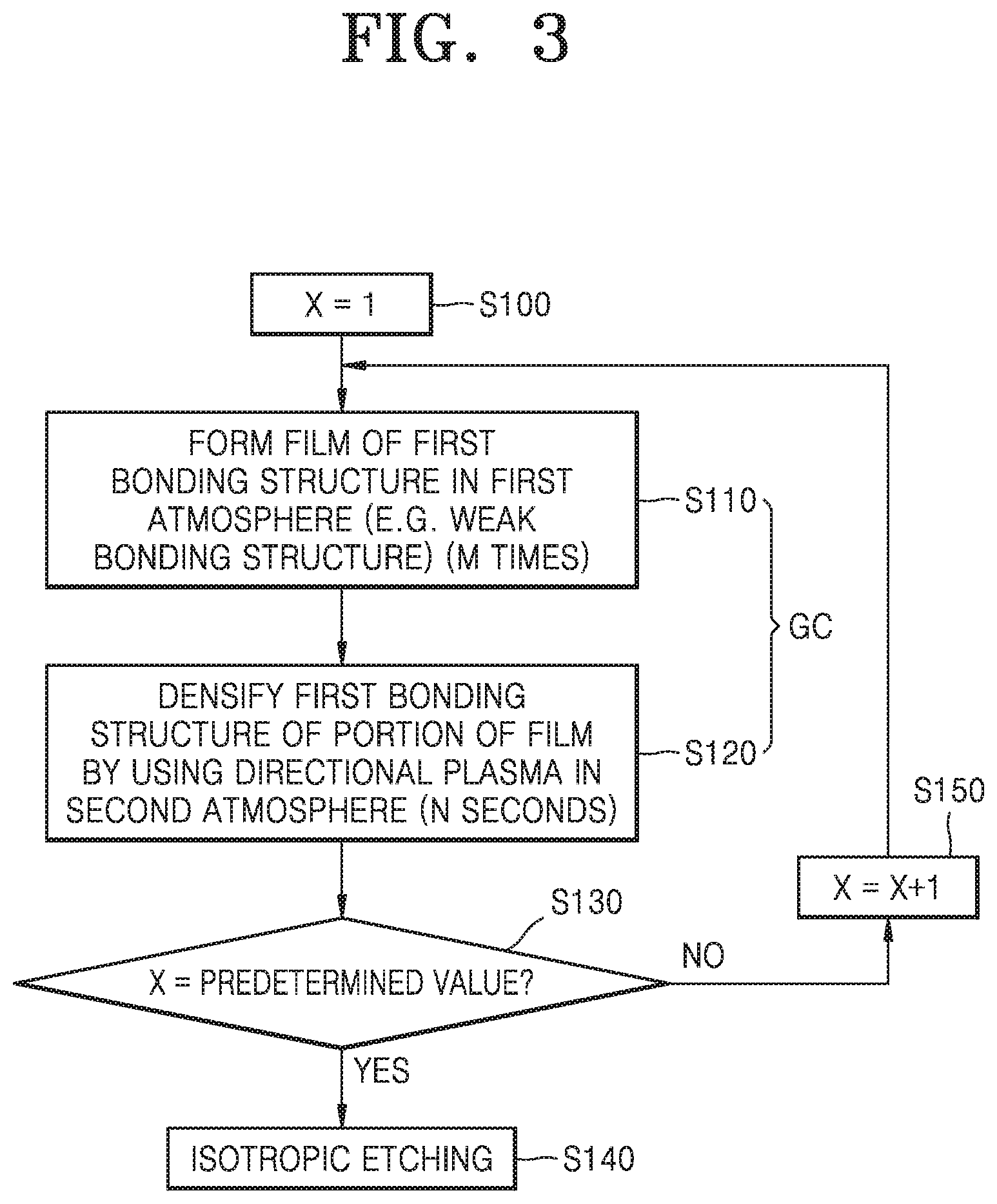
[0072] In contrast with the embodiment of FIG. 2, during the second operation S120 of performing plasma treatment on the film, as shown in FIG. 3, the bonding structure of the film may be densified by plasma ions having directionality in the second atmosphere. For example, plasma ions having components of the film may be provided to the film formed on the top and bottom surfaces of the stepped structure. As a concrete example, when the film is a thin film having Si--N bonds, nitrogen ions may be provided to the top and bottom surfaces of the stepped structure, and accordingly, more Si--N bonds may be created so that the bonding structure of the film may be densified.
[0073] Accordingly, during the subsequent isotropic etching operation S140, the densified portions (for example, the film formed on the top and bottom surfaces of the stepped structure) of the film may remain, and the other portions may be removed, thereby achieving selective etching. According to some embodiments, to more stably perform the selective etching, a film having a second bonding structure (for example, a weak bonding structure) may be formed during the first operation S110.
[0074] FIG. 4 schematically shows a substrate processing method according to embodiments based on a technical concept of the disclosure. The substrate processing method according to the embodiments may be a modified example of the substrate processing method according to the above-described embodiments. Hereinafter, redundant descriptions about the embodiments will be omitted.
[0075] Referring to FIG. 4, X representing the number of times by which a group cycle GC is performed may be set to an initial value of 1, in operation S100, and M representing the number of times by which the first operation S110 of forming the film is performed may also be set to an initial value of 1, in operation S10. Then, the first operation S110 that is performed M-th in a X-th group cycle may be performed. During the first operation that is performed M-th (M=1), a first source gas may be first supplied into a reaction space, in operation S11. The first source gas may be chemisorbed on a surface of a pattern structure (for example, a stepped structure of a high aspect ratio (10:1 or more)) on a substrate, and the first source gas remaining in the reaction space may be purged and removed from the reaction space, in operation S12. Thereafter, a first reaction gas may be supplied into the reaction space. After the first reaction gas is supplied (or, when the first reaction gas is supplied), first plasma treatment may be performed to form a first film, in operation S13. Then, the first reaction gas remaining in the reaction space may be purged and removed from the reaction space, in operation S14.
[0076] Thereafter, M may increase (that is, M=2), and then, the first operation S110 which is performed M-th may be performed. That is, a second source gas may be supplied into the reaction space, in operation S11', and the second source gas remaining in the reaction space may be purged and removed from the reaction space, in operation S12'. Thereafter, a second reaction gas may be supplied into the reaction space, and second plasma treatment may be performed to form a second film, in operation S13'. Then, the second reaction gas remaining in the reaction space may be purged and removed from the reaction space, in operation S14'.
[0077] As such, the first operation S110 may be repeated a plurality of times. The first operation S110 may be performed repeatedly until M reaches a predetermined value. While the first operation S110 is performed repeatedly, the M value may continue to increase. A plurality of films formed by the first operation S110 performed a plurality of times may form a film including the same material.
[0078] After a film of a desired thickness is formed by performing the first operation S110 by a predetermined number of times, the second operation S120 may be performed. During the second operation S120, third plasma treatment may be performed on the formed film. As described above, the first atmosphere of the reaction space in which the first operation S110 is performed may be different from the second atmosphere of the reaction space in which the second operation S120 is performed.
[0079] By the third plasma treatment, a bonding structure of the film formed by the first operation S110 may change (for example, weakening). Thereafter, a group cycle GC including the first operation S110 and the second operation S120 may be performed repeatedly. That is, the X value may increase to 2 from 1, the first operation S110' may be again performed M times, and then, the second operation S120' may be again performed.
[0080] For example, a second group cycle GC that is performed after the X value increases to 2 from 1 may further include operation S11'' of supplying a third source gas onto a second film, operation S12'' of purging the third source gas, an operation S13'' of supplying a third reaction gas and performing fourth plasma treatment to form a third film on the second film, an operation S14'' of purging the third reaction gas, and an operation S120' of performing fifth plasma treatment on the third film.
[0081] The first film and the second film formed during the first operation S110 of the first group cycle GC and the third film formed during the first operation S110' of the second group cycle GC may form a film including the same material. The first operation may continue to be performed to form a fourth deposition film. In another selective embodiment, the number of times by which the first operation is performed during a group cycle may be different for each group cycle.
[0082] After the third film and/or the fourth film is formed, fifth plasma treatment may be performed. By the fifth plasma treatment, a bonding structure of the third film and/or the fourth film may change. In other words, by the third plasma treatment (operation S120) of the first group cycle and the fifth plasma treatment (operation S120') of the second group cycle, a bonding structure of a portion of the deposition film may change.
[0083] For example, when a silicon nitride film is formed on a stepped structure having a top surface, a bottom surface, and a side surface connecting the top surface and the bottom surface, plasma ions of strong power may be injected into the film. Then, a Si--N bonding structure of the silicon nitride film may be broken. Because the plasma ions have directionality (vertical directionality toward a susceptor located below from a shower head located above), the bonding structure of the film formed on the top and bottom surfaces of the stepped structure may be weakened.
[0084] According to embodiments based on a technical concept of the disclosure, when a film of a predetermined thickness is formed, a portion of the film may be formed in some group cycles among a plurality of group cycles, and the remaining portion of the film may be formed in the remaining group cycles. Also, plasma treatment may be performed on a portion of the film during each group cycle. As such, by repeatedly performing a group cycle for forming a portion of a film and performing plasma treatment on the portion of the film, instead of depositing a film of a predetermined thickness and performing plasma treatment on the entire deposition film, an etch selectivity between the film formed on the top and bottom surfaces of the stepped structure and the film formed on the side surface of the stepped structure may be improved.
[0085] According to some embodiments, during the first plasma treatment (operation S13) and the second plasma treatment (operation S13') of the first group cycle and the fourth plasma treatment (operation S13'') of the second group cycle for forming the conformal deposition film, the first atmosphere of the reaction space may be set such that plasma ions have no directionality. For example, the first plasma treatment (operation S13), the second plasma treatment (operation S13'), and the fourth plasma treatment (operation S13'') may be performed under first pressure (that is, high pressure of, for example, 10 Torr to 20 Torr). As another example, during the first plasma treatment (operation S13), the second plasma treatment (operation S13'), and the fourth plasma treatment (operation S13''), first power (that is, low power of, for example, 200 W to 500 W) may be supplied.
[0086] In contrast, during the third plasma treatment (operation S120) of the first group cycle and the fifth plasma treatment (operation S120') of the second group cycle, the second atmosphere of the reaction space may be set such that the plasma ions have directionality. For example, the third plasma treatment (operation S120) and the fifth plasma treatment (operation S120') may be performed under second pressure (that is, low pressure of, for example, 1 Torr to 5 Torr) that is lower than the first pressure. As another example, during the third plasma treatment (operation S120) and the fifth plasma treatment (operation S120'), second power (that is, high power of, for example, 700 W to 1000 W) that is higher than the first power may be supplied.
[0087] FIG. 5 schematically shows a substrate processing method according to embodiments based on a technical concept of the disclosure.
[0088] Referring to FIG. 5, the substrate processing method may include a first operation that is performed a plurality of times. In the first operation, a source gas (for example, a silicon source) may be supplied for t0 to t1, the remaining source gas may be purged for t1 to t3, a reaction gas supplied to function as a purge gas and a reaction gas may be excited by plasma application to react with the source gas to form a film for t3 to t7, and the remaining reaction gas may be purged for t7 to t8. The first operation may be performed repeatedly so that a film of a predetermined thickness may be formed on a stepped structure.
[0089] For example, to deposit a SiN film on a stepped structure of a substrate, a Si-containing precursor and a N2 gas may be supplied, and when plasma is supplied, the N2 gas may be ionized to react with the Si-containing precursor to form a thin film. Although the N2 gas continues to be supplied, the N2 gas may be ionized under plasma to function as a reactive purge gas reacting with a source gas.
[0090] In the first operation, process pressure may be maintained at 3 Torr or lower and a power value may be maintained at 900 W or higher such that a conformal deposition film is formed and simultaneously, a portion of the film formed on the stepped structure is weakened. However, the process condition may result in incomplete etching upon subsequent isotropic etching performed on the film formed on the stepped structure (see FIG. 6).
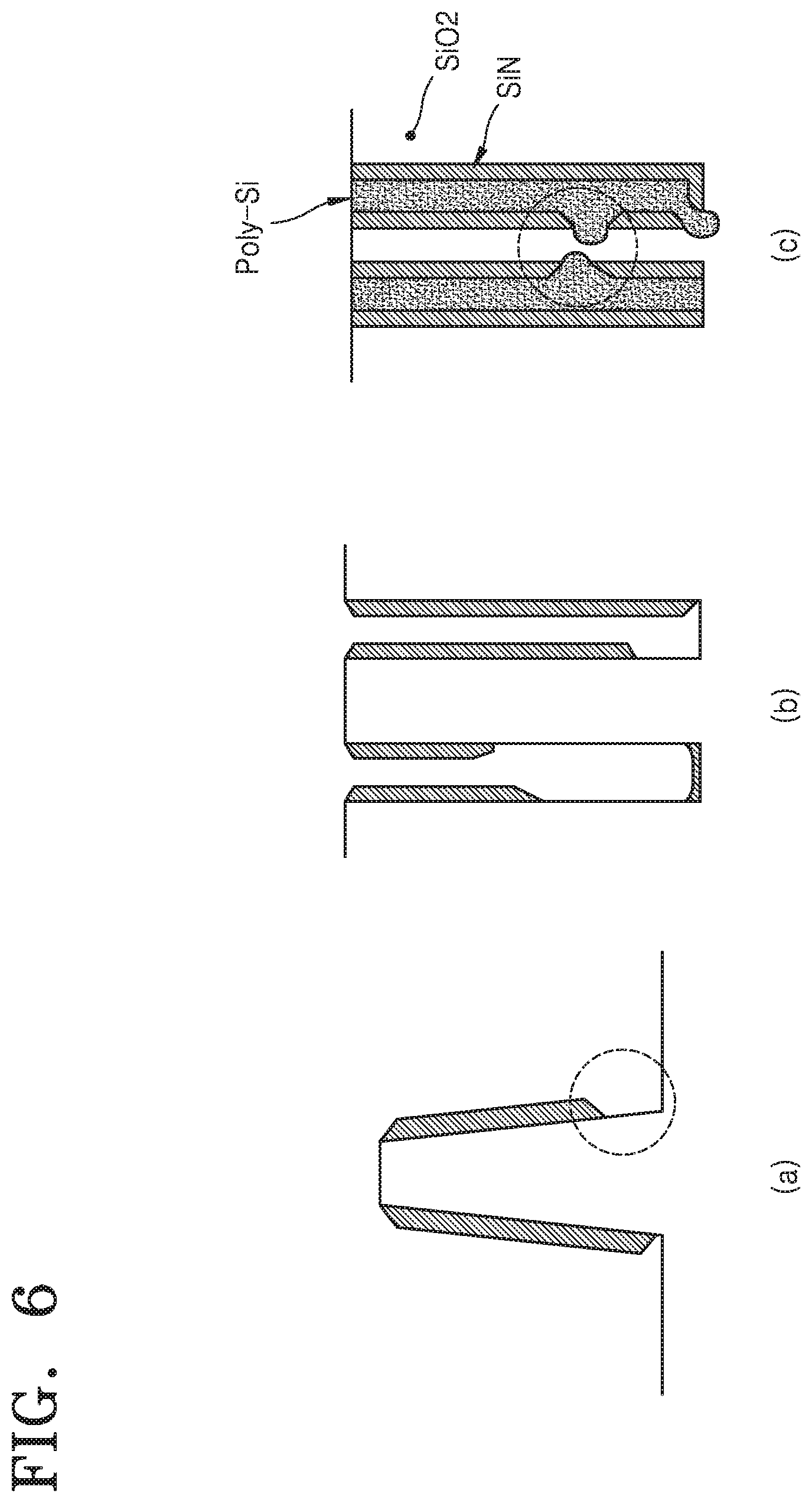
[0091] (a) of FIG. 6 shows an example in which a film (for example, a SiN film) is lost in a part of a side portion of a step. (b) of FIG. 6 shows an example in which a film (for example, a SiN film) is lost in a part of a side portion of a stepped structure having a great aspect ratio (for example, an aspect ratio >10:1), and a film (for example, a SiN film) remains in a bottom portion of a step. (c) of FIG. 6 shows a case in which a film (for example, a SiN film) formed on a part of a side portion of a step is lost and over-etch occurs in the inside (SiO.sub.2 film) of a stepped structure in an etching operation after film deposition. In the case of (c) of FIG. 6, when a conductive material (for example, poly Si) is filled in a subsequent process, an electrical short with the conductive material filled in the neighboring step may occur.
[0092] According to embodiments based on a technical concept of the disclosure for preventing the incomplete selective etching, a first operation of evenly depositing a firm and uniform film on a stepped structure and a second operation of performing plasma treatment to increase an etching selectivity of a film deposited on the side and top/bottom portions of a step may be performed.
[0093] FIGS. 7 and 8 schematically show a substrate processing method according to embodiments based on a technical concept of the disclosure. The substrate processing method according to the embodiments may be a modified example of the substrate processing method according to the above-described embodiments. Hereinafter, redundant descriptions about the embodiments will be omitted.
[0094] The embodiments based on the technical concept of the disclosure propose a method of preventing loss of a film deposited on a side portion of a step. More specifically, a method of increasing a strength and chemical resistance of a film to increase an etch selectivity between the film deposited on the top/bottom portion of a step and the film deposited on the side portion of the step may be proposed to prevent the film deposited on the side portion of the step from being easily lost.
[0095] Referring to FIGS. 7 and 8, in a first operation (t0 to t8) which is an operation of evenly depositing a hard and uniform film (for example, a SiN film) on a stepped structure, the film may be deposited by a PEALD process. The first operation may be performed repeatedly m times. A second operation (t8 to t15), which is a plasma treatment operation, may be performed repeatedly for n seconds. A group cycle operation consisting of the first operation and the second operation may be performed repeatedly a plurality of times (for example, x cycles).
[0096] In the first operation, a hard and conformal film (for example, a SiN film) may be deposited on the stepped structure under conditions of high pressure (for example, 15 Torr) and relatively low plasma power (for example, 500 watt). Because a large amount of gas exists (that is, high pressure) and plasma is relatively weak (that is, low power) in a reaction space, a mean free path of radical ions may decrease and random movements of the radical ions may increase. Accordingly, the ions may be evenly distributed on the top/bottom and side portions of the stepped structure so that reactions between a substrate surface and ion radicals occur uniformly over the entire surface without being biased to a certain surface of a step, and therefore, a hard and uniform film (conformal film) may be deposited.
[0097] In the second operation, plasma may be supplied for a predetermined time period under conditions of pressure that is relatively lower than in the first operation and plasma power that is relatively higher than in the first operation to increase an ion bombardment effect of plasma ions. For example, in the second operation, process pressure may be 3 Torr and plasma may be about 900 watt. To keep internal pressure of a chamber at low pressure, reducing an amount of a reaction gas may be used as necessary. Because directionality (straightness) of radical ions is reinforced, unlike the first operation, a bonding structure of a film (for example, a SiN film) deposited on a certain surface of the step, for example, on the top/bottom portion of the step, which is perpendicular to a traveling direction of radicals, may be weakened by ion bombardment. The first operation and the second operation may form a group cycle, and the group cycle may be performed repeatedly x times to deposit a desired film thickness. Thereafter, isotropic etching (for example, wet etching) may be performed to remove the film formed on the top/bottom surface of the stepped structure while maintaining the film formed on the side wall.
[0098] Table 1 shows process conditions according to the embodiments based on the technical concept of the disclosure, in detail.
TABLE-US-00001 TABLE 1 First Operation Second Operation (Conformal (Plasma Deposition) Treatment) Gas Flow Si Source 1000~2000 0 (sccm) (Carrier N2) N2 (Reactive Purge) 10000~20000 1000~2000 Processing Source Supply 0.15~0.7 0 Time Source Purge 0.5~1.sup. 0 (sec) Plasma 1~5 5~60 Purge 0.1~0.3 0 Number of 10~50 -- Times of Cycles Plasma Power (W) 200~500 700~1000 Frequency (Hz) 13.56M 13.56M Pressure (Torr) 10~20 1~5 Heater Temperature (.degree.C.) 300~550 300~550
[0099] In Table 1, comparing the first operation with the second operation, a larger amount of gas may be supplied at a rate of 5:1 to maximally 20:1 in the first operation. By setting a supply time of plasma to 1:1 to maximally 1:60, plasma power to 1:3.5 to maximally 1:5, and process pressure to 2:1 to maximally 20:1, the first operation may decrease a mean free path of radical ions to deposit a uniform and hard film on the stepped structure, and the second operation may increase the straightness and ion bombardment effect of the radical ions to weaken the bonding structure of the film deposited on the top/bottom surface of the stepped structure. Accordingly, the film deposited on the side portion of the step in the first operation may be hardened, thereby being prevented from being lost in a subsequent etching operation.
[0100] FIG. 9 shows a result after the substrate processing method according to the embodiments of FIGS. 7 and 8 is performed by depositing a SiN film on a stepped structure and performing a subsequent etching process according to the process conditions shown in Table 1.
[0101] As shown in FIG. 9, the SiN film on the side wall of the step is maintained at a constant thickness without being lost even at a boundary between the side wall and the bottom wall of the step, whereas the SiN film on the bottom surface of the step is selectively removed.
[0102] Furthermore, according to embodiments based on a technical concept of the disclosure, by changing a film material of the film formed on the top and bottom portions of the step while maintaining a film material of the film on the side portion of the step, various forms of RTS (reverse topo-selective) process windows may be secured. More specifically, by adjusting a plasma processing condition of the second operation, a wet etch selectivity between the top/bottom portion of the step and the side portion of the step may be arbitrarily adjusted, and a film profile after etching may be adjusted.
[0103] As an example related to the adjustment of selectivity, Table 2 shows etch selectivities of the top and side surfaces of a step according to the numbers of repetitions of the first operation and plasma treatment times of the second operation. When the number of repetitions of the first operation is m (times) and the treatment time of the second operation is n (seconds), subsequent wet etching rates according to changes of m and n are as follows.
TABLE-US-00002 TABLE 2 Conformal Treatment 1 Treatment 2 Deposition (m: 40 cy, (m: 20 cy, (No treatment) n: 1 min) n: 1 min) Top Film WER 2.4 16.3 67 (A/sec) Side Film WER 2 2.4 2.6 (A/sec) Selectivity 1.2 6.8 25.8 (Top Portion/ Side Portion WER)
[0104] In the Table 2, the conformal deposition condition represents a case in which the first operation is performed without the second operation. The Treatment 1 condition (TRT1) represents a case in which the first operation is performed 40 times (40 cycles) and the second operation is performed for 1 minute (60 seconds). The Treatment 2 condition (TRT2) represents a case in which the first operation is performed 20 times (20 cycles) and the second operation is performed for 1 minute (60 seconds).
[0105] As shown in Table 2, as a ratio of the second operation to the first operation increases, a selectivity between the top portion and the side portion in the stepped structure increases. That is, Table 2 shows that a highest WER selectivity of 25.8 is obtained under the Treatment 2 condition. In other words, compared with the conformal deposition condition, the SiN film on the top portion of the step is quickly etched, whereas the SiN film on the side portion of the step is little etched, under the Treatment 2 condition (TRT2). Therefore, a higher etch selectivity may be achieved.
[0106] FIG. 10 shows SiN films on steps after wet etching is performed according to the conditions (that is, the conformal deposition condition, the Treatment 1 condition, and the Treatment 2 condition) of Table 2.
[0107] Referring to FIG. 10, the conformal deposition condition represents a case in which the first operation is applied without the second operation to deposit a conformal SiN film in a stepped structure. In the conformal deposition condition, high process pressure and low plasma power may be applied. Accordingly, radical ions may be evenly distributed on the entire of the stepped structure, and even after wet etching, a hard SiN film of a constant thickness may remain evenly on the top, side, and bottom portions of a step (see a left part of FIG. 10).
[0108] Then, in the Treatment 1 condition (TRT1), the first operation may be performed for 40 cycles, and then, plasma treatment of the second operation may be performed for 1 minute. As shown in the middle part of FIG. 10, a SiN film formed on a side portion remains as it is, and a SiN film formed on a bottom portion is partially removed. However, in the bottom portion of the stepped structure, a SiN film may still remain.
[0109] Finally, under the Treatment 2 condition (TRT 2), the first operation may be performed for 20 cycles, and then plasma treatment of the second operation may be performed for 1 minute. That is, by increasing a ratio of the second operation to the first operation, a SiN film formed on a side portion of a step is maintained with its original thickness without being lost, and a SiN film formed on a bottom portion of the step is removed, after etching (see a right part of FIG. 10). As such, by appropriately adjusting a ratio of the first operation and the second operation, a substrate processing process with an improved thickness adjustment function may be implemented.
[0110] FIG. 11 illustrates the process.
[0111] As shown in FIG. 11, by increasing a ratio of the second operation to the first operation, a profile of a SiN film may be adjusted. For example, when the second operation is not performed (a left part of FIG. 11), a SiN film formed on a bottom surface of a pattern PTN remains as it is even after isotropic etching. Meanwhile, when the second operation is performed at relatively low frequency (a middle part of FIG. 11), a SiN film formed on a bottom surface of a pattern PTN is partially removed after isotropic etching so that a portion of the bottom surface of the pattern PTN is exposed. Also, when the second operation is performed at relatively high frequency (a right part of FIG. 11), a SiN film formed on a bottom surface of a pattern PTN is completely removed after isotropic etching so that the entire bottom surface of the pattern PTN is exposed.
[0112] As such, a profile of a SiN film formed on bottom and side portions of a step may be controlled according to treatment times of a plasma treatment operation. Accordingly, various shapes of thin film profiles may be implemented according to application targets. For wiring of top/bottom portions in a device, a bottom film formed on a step may be removed. Also, by opening a portion of a bottom film, a device with more improved performance may be manufactured.
[0113] FIG. 12 schematically shows a substrate processing method according to embodiments based on a technical concept of the disclosure. The substrate processing method according to the embodiments may be a modified example of the substrate processing method according to the above-described embodiments. Hereinafter, redundant descriptions about the embodiments will be omitted.
[0114] Referring to FIG. 12, the embodiments based on the technical concept of the disclosure propose a substrate processing method of processing a substrate by performing a plurality of group cycles, and the substrate processing method may selectively etch a thin film on a pattern PTN through isotropic etching (for example, wet etching) without performing an additional photolithography process.
[0115] A group cycle may include a plurality of deposition cycles and plasma treatment, and while the plurality of deposition cycles are performed, a conformal deposition film having a low subsequent wet etching rate WER may be formed on a stepped structure. By performing strong plasma treatment on the film formed after the plurality of deposition cycles, a bonding structure of a portion of the film formed on the top and bottom portions of the stepped structure may change. The change of the bonding structure may result in an increase of the subsequent wet etching rate WER.
[0116] After a group cycle terminates by performing the plurality of deposition cycles and strong plasma treatment, the next group cycle may be performed so that a plurality of deposition cycles and strong plasma treatment are again performed repeatedly. As such, a plurality of group cycles may be performed to form a film with a predetermined thickness, in such a way to form a film and perform plasma treatment on a portion of the film in each group cycle, thereby forming a film with an improved etch selectivity. As a result, a patterned film may be formed on a stepped structure having a high aspect ratio, without performing a lithography process.
[0117] It should be understood that embodiments described herein should be considered in a descriptive sense only and not for purposes of limitation. Descriptions of features or aspects within each embodiment should typically be considered as available for other similar features or aspects in other embodiments.
[0118] While one or more embodiments have been described with reference to the figures, it will be understood by those of ordinary skill in the art that various changes in form and details may be made therein without departing from the spirit and scope of the disclosure as defined by the following claims.
* * * * *
D00000
D00001
D00002
D00003
D00004
D00005
D00006
D00007
D00008
D00009
D00010
D00011
D00012

XML
uspto.report is an independent third-party trademark research tool that is not affiliated, endorsed, or sponsored by the United States Patent and Trademark Office (USPTO) or any other governmental organization. The information provided by uspto.report is based on publicly available data at the time of writing and is intended for informational purposes only.
While we strive to provide accurate and up-to-date information, we do not guarantee the accuracy, completeness, reliability, or suitability of the information displayed on this site. The use of this site is at your own risk. Any reliance you place on such information is therefore strictly at your own risk.
All official trademark data, including owner information, should be verified by visiting the official USPTO website at www.uspto.gov. This site is not intended to replace professional legal advice and should not be used as a substitute for consulting with a legal professional who is knowledgeable about trademark law.