Method Of Depositing Thin Film And Method Of Manufacturing Semiconductor Device
Kim; Young Hoon ; et al.
U.S. patent application number 16/897158 was filed with the patent office on 2020-09-24 for method of depositing thin film and method of manufacturing semiconductor device. The applicant listed for this patent is ASM IP HOLDING B.V.. Invention is credited to Yong Gyu Han, Dae Youn Kim, Young Hoon Kim, Wan Gyu Lim, Tae Hee Yoo, Jin Geun Yu.
| Application Number | 20200303180 16/897158 |
| Document ID | / |
| Family ID | 1000004885400 |
| Filed Date | 2020-09-24 |


View All Diagrams
| United States Patent Application | 20200303180 |
| Kind Code | A1 |
| Kim; Young Hoon ; et al. | September 24, 2020 |
METHOD OF DEPOSITING THIN FILM AND METHOD OF MANUFACTURING SEMICONDUCTOR DEVICE
Abstract
Provided is a method of depositing a thin film on a pattern structure of a semiconductor substrate, the method including (a) supplying a source gas; (b) supplying a reactive gas; and (c) supplying plasma, wherein the steps (a), (b), and (c) are sequentially repeated on the semiconductor substrate within a reaction space until a desired thickness is obtained, and a frequency of the plasma is a high frequency of 60 MHz or greater.
| Inventors: | Kim; Young Hoon; (Chungcheongnam-do, KR) ; Han; Yong Gyu; (Seoul, KR) ; Kim; Dae Youn; (Daejeon, KR) ; Yoo; Tae Hee; (Gyeonggi-do, KR) ; Lim; Wan Gyu; (Gyeonggi-do, KR) ; Yu; Jin Geun; (Chungcheongnam-do, KR) | ||||||||||
| Applicant: |
|
||||||||||
|---|---|---|---|---|---|---|---|---|---|---|---|
| Family ID: | 1000004885400 | ||||||||||
| Appl. No.: | 16/897158 | ||||||||||
| Filed: | June 9, 2020 |
Related U.S. Patent Documents
| Application Number | Filing Date | Patent Number | ||
|---|---|---|---|---|
| 15949990 | Apr 10, 2018 | 10714335 | ||
| 16897158 | ||||
| Current U.S. Class: | 1/1 |
| Current CPC Class: | C23C 16/45542 20130101; H01L 21/02208 20130101; C23C 16/50 20130101; H01L 21/31111 20130101; H01L 21/0332 20130101; H01L 21/02274 20130101; H01L 21/02164 20130101; H01L 21/0338 20130101; H01L 21/31144 20130101; H01L 21/0337 20130101; H01L 21/0228 20130101; C23C 16/345 20130101; H01L 21/0217 20130101; H01L 21/02211 20130101; H01L 21/02219 20130101; C23C 16/45525 20130101 |
| International Class: | H01L 21/02 20060101 H01L021/02; H01L 21/033 20060101 H01L021/033; H01L 21/311 20060101 H01L021/311; C23C 16/50 20060101 C23C016/50; C23C 16/455 20060101 C23C016/455; C23C 16/34 20060101 C23C016/34 |
Foreign Application Data
| Date | Code | Application Number |
|---|---|---|
| Apr 25, 2017 | KR | 10-2017-0053228 |
| Mar 22, 2018 | KR | 10-2018-0033495 |
Claims
1. A method of depositing a thin film on a pattern structure of a semiconductor substrate, the method comprising: (a) supplying a source gas; (b) supplying a reactive gas; and (c) supplying plasma, wherein the steps (a), (b), and (c) are sequentially repeated on the semiconductor substrate within a reaction space until a desired thickness is obtained, and a frequency of the plasma is a frequency of at least 60 MHz or greater, wherein the pattern structure has a top surface, a bottom surface, and a side surface that connects the top surface with the bottom surface, a length of the side surface being greater than a width of the top surface and a width of the bottom surface, the frequency of at least 60 MHz or greater is used to form the thin film having a uniform physical thickness and a uniform chemical characteristics on an entire area of the top surface, the bottom surface, and the side surface of the pattern structure, wherein, in the step (c), the plasma is supplied in a pulse mode, and an overall amount of plasma supplied is equal to an amount of the plasma supplied in a continuous mode, and wherein at least one of materials used during the depositing the thin film has reactivity with the pattern structure, so that at least a portion of the pattern structure is damaged during the step (c), generating a difference between critical dimensions (CDs) of an inner space and an outer space of the pattern structure, wherein, in order to decrease loss of the pattern structure, the plasma is supplied onto the semiconductor substrate at a duty ratio of less than 100%, and the plasma is supplied at a power amount more than that of the plasma supplied in the continuous mode.
2. The method of claim 1, wherein the plasma is supplied onto the semiconductor substrate at a duty ratio of 50%, and the plasma is supplied at a power amount twice that of the plasma supplied in the continuous mode.
3. The method of claim 1, wherein an Si source is used for the source gas.
4. The method of claim 3, wherein the Si source includes at least one of DIPAS, TSA, (SiH3)3N; DSO, (SiH3)2; DSMA, (SiH3)2NMe; DSEA, (SiH3)2NEt; DSIPA, (SiH3)2N(iPr); DSTBA, (SiH3)2N(tBu); DEAS, SiH3NEt2; DTBAS, SiH3N(tBu)2; BDEAS, SiH2(NEt2)2; BDMAS, SiH2(NMe2)2; BTBAS, SiH2(NHtBu)2; BITS, SiH2(NHSiMe3)2; TEOS, Si(OEt)4; SiCl4; HCD, Si2Cl6; 3DMAS, SiH(N(Me)2)3; BEMAS, Si H2[N(Et)(Me)]2; AHEAD, Si2 (NHEt)6; TEAS, Si(NHEt)4; Si3H8; DCS, SiH2Cl2; SiHI3; SiH2I2.
5. The method of claim 1, wherein an oxygen source is used for the forming the second silicon oxide mask layer.
6. The method of claim 5, wherein the oxygen source includes at least one of O2, O3, N2O, and CO2.
7. The method of claim 1, a purge gas is continuously supplied in all of the steps (a), (b), and (c).
8. The method of claim 7, wherein the reactive gas is continuously supplied in all of the steps (a), (b), and (c), the reactive gas comprises a constituent of the thin film, and, when the reactive gas is not activated by the plasma, the reactive gas is inert to the source gas.
9. The method of claim 8, wherein, after the step (c), the purge gas and the reactive gas are further supplied.
10. The method of claim 1, wherein, during the step (c), at least a portion of the pattern structure is removed.
11. The method of claim 1, wherein the plasma is supplied at a power in a range of 200 watts to 2,000 watts.
12. The method of claim 1, further comprising wet-etching the thin film deposited on the pattern structure.
13. The method of claim 1, wherein a ratio between wet etch rates (WERs) of portions of the thin film respectively deposited on a sidewall and a top of the pattern structure is 1.5 or less.
14. The method of claim 1, wherein the pattern structure of the semiconductor substrate comprises a hardmask.
15. A thin film deposition method comprising: preparing a substrate comprising a thin film and a first mask pattern formed on the thin film; and forming a second silicon oxide mask layer on an exposed surface of the thin film and on the first mask pattern, wherein the forming of the second silicon oxide mask layer is performed by applying plasma at a frequency of 60 MHz or greater by using a plasma-enhanced deposition process, and the plasma is discontinuously applied, wherein the first mask pattern has a top surface, a bottom surface, and a side surface that connects the top surface with the bottom surface, a length of the side surface being greater than a width of the top surface and a width of the bottom surface, wherein the frequency of 60 MHz or greater is used to form the second silicon oxide mask layer having a uniform physical thickness and a uniform chemical characteristics on an entire area of the top surface, the bottom surface, and the side surface of the first mask pattern, wherein, during the applying plasma, the plasma is supplied in a pulse mode, and an overall amount of plasma supplied in the pulse mode is equal to an amount of the plasma supplied in a continuous mode, and wherein at least one of materials used during the plasma-enhanced deposition process has reactivity with the first mask pattern, so that at least a portion of the first mask pattern is damaged during the applying plasma in the forming of the second silicon oxide mask layer, generating a difference between critical dimensions (CDs) of an inner space and an outer space of the first mask pattern.
16. The method of claim 15, wherein the plasma-enhanced deposition process includes a plasma-enhanced atomic layer deposition (PEALD) process.
17. A method of manufacturing a semiconductor device, the method comprising: forming a first layer on a substrate; forming a second layer on the first layer; exposing at least a portion of the first layer by patterning the second layer; forming a third layer on an exposed surface of the first layer and on the second layer, wherein the forming of the third layer is performed by applying plasma at a frequency of 60 MHz or greater by using a plasma-enhanced deposition process; and forming a spacer pattern by removing at least a portion of the third layer, wherein, during the applying plasma, the plasma is supplied in a pulse mode, and an overall amount of plasma supplied is equal to an amount of the plasma supplied in a continuous mode, and wherein at least one of materials used during the plasma-enhanced deposition process has reactivity with the patterned second layer, so that at least a portion of the patterned second layer is damaged during the applying plasma in the forming of the third layer, generating a difference between critical dimensions (CDs) of an inner space and an outer space of the patterned second layer, wherein, in order to decrease loss of the patterned second layer that is below the third layer, the plasma having the frequency of 60 MHz or greater is supplied onto the substrate at a duty ratio of less than 100%, and the plasma is supplied at a power amount larger than that of the plasma supplied in the continuous mode.
18. The method of claim 17, wherein the patterned second layer has a top surface, a bottom surface, and a side surface that connects the top surface with the bottom surface, a length of the side surface being greater than a width of the top surface and a width of the bottom surface.
19. The method of claim 18, wherein the frequency of 60 MHz or greater is used to form the third layer having a uniform physical thickness and a uniform chemical characteristics on an entire area of the top surface, the bottom surface, and the side surface of the patterned second layer.
20. The method of claim 17, further comprising: removing the second layer; and etching the first layer by using the spacer pattern as a mask.
Description
CROSS-REFERENCE TO RELATED APPLICATION
[0001] This is a continuation of U.S. patent application Ser. No. 15/949,990, filed Apr. 10, 2018, which claims the benefit of Korean Patent Application No. 10-2017-0053228, filed on Apr. 25, 2017, in the Korean Intellectual Property Office, the disclosure of which is incorporated herein in its entirety by reference. In addition, the application claims the benefit of Korean Patent Application No. 10-2018-0033495, filed on Mar. 22, 2018, in the Korean Intellectual Property Office, the disclosure of which is incorporated herein in its entirety by reference.
BACKGROUND
1. Field
[0002] One or more embodiments relate to a method of depositing a thin film and a method of manufacturing a semiconductor device, and more particularly, to a method of depositing a thin film on a pattern structure on a substrate via plasma-enhanced atomic layer deposition (PEALD), and a method of manufacturing a semiconductor device.
2. Description of the Related Art
[0003] Recently, due to the miniaturization of semiconductor devices, an atomic layer deposition process for depositing a uniform thin film is being widely used. In many cases, semiconductor thin film processes are conducted at high temperature, which results in a thermal shock or thermal budget which degrades performance of semiconductor devices. Accordingly, a plasma-enhanced atomic layer deposition (PEALD) method capable of depositing a thin film at low temperature and precisely controlling the deposition has been introduced, and the range of applications for PEALD has gradually widened.
SUMMARY
[0004] One or more embodiments include a method for depositing a thin film of a uniform film quality on a top and a sidewall of a step in a semiconductor pattern structure, and enhancing conformality of a wet etch rate (WER) in a subsequent wet etching process.
[0005] One or more embodiments include a substrate processing method for enhancing conformality of a WER and also preventing damage of a lower pattern structure and thus enhancing critical dimension (CD) uniformity.
[0006] Additional aspects will be set forth in part in the description which follows and, in part, will be apparent from the description, or may be learned by practice of the presented embodiments.
[0007] According to one or more embodiments, a method of depositing a thin film on a pattern structure of a semiconductor substrate includes (a) supplying a source gas; (b) supplying a reactive gas; and (c) supplying plasma, wherein the steps (a), (b), and (c) are sequentially repeated on the semiconductor substrate within a reaction space until a desired thickness is obtained, and a frequency of the plasma is a high frequency of 60 MHz or greater.
[0008] A purge gas may be continuously supplied in all of the steps (a), (b), and (c).
[0009] The reactive gas may be continuously supplied in all of the steps (a), (b), and (c), the reactive gas may include a constituent of the thin film, and, when the reactive gas is not activated by the plasma, the reactive gas may be inert to the source gas.
[0010] After the step (c), the purge gas and the reactive gas may be further supplied.
[0011] During the step (c), at least a portion of the pattern structure may be removed.
[0012] In the step (c), the plasma may be supplied in a continuous mode.
[0013] In the step (c), the plasma may be supplied in a pulse mode, and an overall amount of plasma supplied may be equal to an amount of the plasma supplied in a continuous mode.
[0014] The plasma may be supplied onto the semiconductor substrate at a duty ratio of 50%, and the plasma may be supplied at a power amount twice that of the plasma supplied in the continuous mode. For example, the plasma may be supplied at a power in a range of 200 watts to 2,000 watts.
[0015] The plasma may be supplied onto the semiconductor substrate at a duty ratio of 25%, and the plasma may be supplied at a power amount four times that of the plasma supplied in the continuous mode. For example, the plasma may be supplied at a power in a range of 400 watts to 4,000 watts.
[0016] The method may further include wet-etching the thin film deposited on the pattern structure.
[0017] A ratio between wet etch rates (WERs) of portions of the thin film respectively deposited on a sidewall and a top of the pattern structure may be 1.5 or less.
[0018] The pattern structure of the semiconductor substrate may include a hardmask.
[0019] According to one or more embodiments, a thin film deposition method includes preparing a substrate including a thin film and a first mask pattern formed on the thin film; and forming a second mask layer on an exposed surface of the thin film and on the first mask pattern, wherein the forming of the second mask layer is performed by applying plasma at a frequency of 60 MHz or greater by using a plasma-enhanced atomic layer deposition (PEALD) process, and the plasma is discontinuously applied.
[0020] At least one of materials used during the PEALD process may have reactivity with the first mask pattern.
[0021] The plasma may be discontinuously applied during all of a plurality of sub-periods, and, during each of the plurality of sub-periods, plasma may be applied at a duty ratio of 50% or less.
[0022] According to one or more embodiments, a method of manufacturing a semiconductor device includes forming a first layer on a substrate; forming a second layer on the first layer; exposing at least a portion of the first layer by patterning the second layer; forming a third layer on an exposed surface of the first layer and on the second layer, wherein the forming of the third layer is performed by applying plasma at a frequency of 60 MHz or greater by using a plasma-enhanced atomic layer deposition (PEALD) process; and forming a spacer pattern by removing at least a portion of the third layer.
[0023] The method may further include removing the second layer; and etching the first layer by using the spacer pattern as a mask.
[0024] The plasma having the frequency of 60 MHz or greater may be discontinuously applied during a plurality of sub-periods.
BRIEF DESCRIPTION OF THE DRAWINGS
[0025] These and/or other aspects will become apparent and more readily appreciated from the following description of the embodiments, taken in conjunction with the accompanying drawings in which:
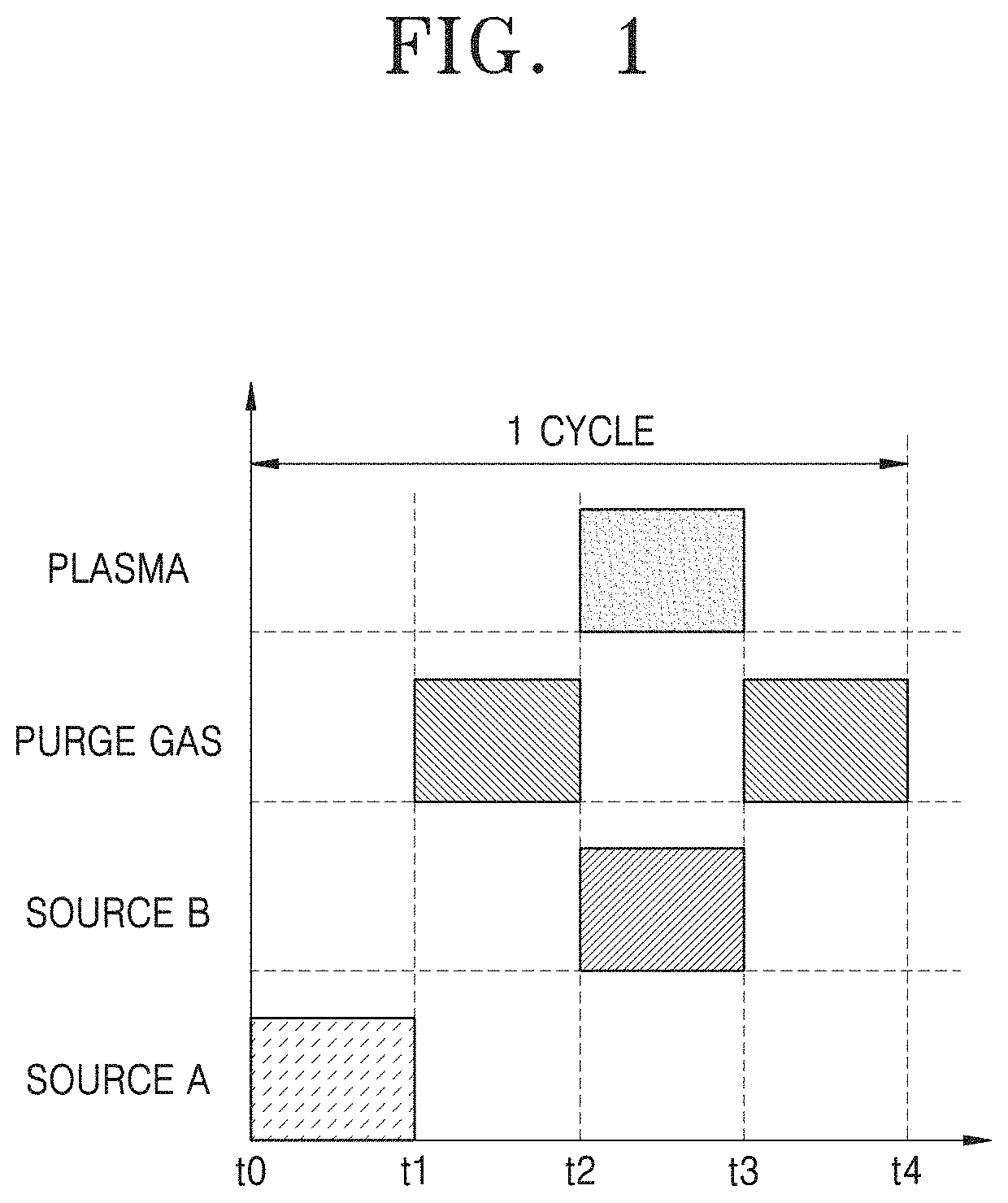
[0026] FIG. 1 is a schematic timing diagram for illustrating a thin film deposition method according to embodiments of the inventive concept;
[0027] FIG. 2 illustrates damage to a mask pattern;
[0028] FIG. 3 is a schematic timing diagram for illustrating a thin film deposition method according to embodiments of the inventive concept;
[0029] FIG. 4 shows process parameters that may be used when a silicon (Si) oxide layer is deposited;
[0030] FIG. 5 is a table illustrating transmission electron microscopy (TEM) images showing step coverage of a thin film on a pattern structure before and after wet etching, and wet etch rate (WER) conformality corresponding to a comparison between WERs of portions of the thin film on a sidewall and a top of the pattern structure after wet etching;
[0031] FIG. 6 is a graph showing a result of a WER experiment on portions of a Si oxide layer respectively deposited on a top, a bottom, and a sidewall of a pattern structure;
[0032] FIGS. 7-9 are schematic timing diagrams for illustrating a thin film deposition method according to embodiments of the inventive concept;
[0033] FIGS. 10 and 11 are graphs showing WERs of a film and loss of a lower film of a pattern structure according to duty ratios when plasma is supplied onto a substrate in a continuous mode and a pulse mode;
[0034] FIGS. 12-15 are schematic cross-sectional views for illustrating a method of manufacturing a semiconductor device, according to embodiments of the inventive concept;
[0035] FIGS. 16-18 are graphs showing loss of a spin-on-hardmask (SOH) generated when a plasma process is performed;
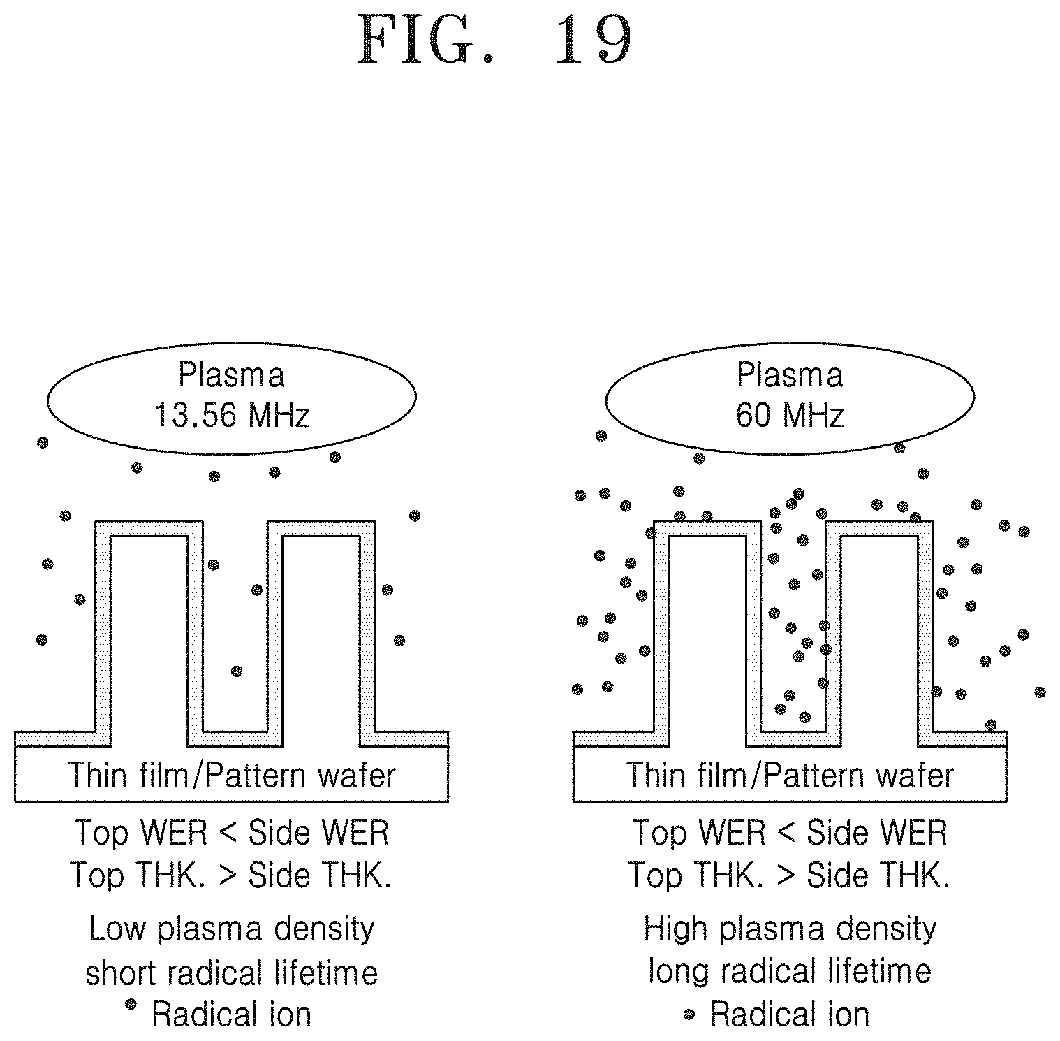
[0036] FIG. 19 illustrates behaviors of plasma on a pattern structure in plasma processes of 13.56 MHz and 60 MHz;
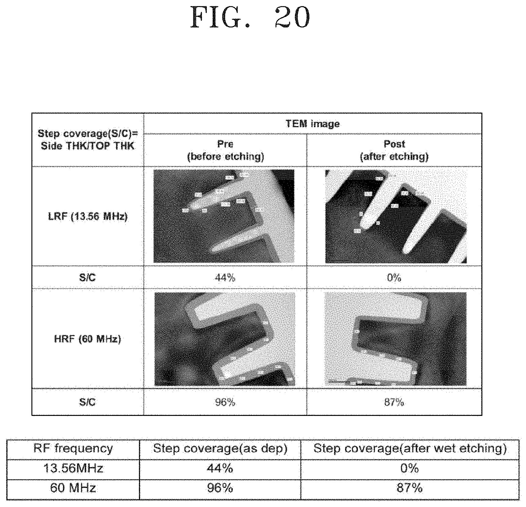
[0037] FIG. 20 is a table showing transmission electron microscopy (TEM) images showing an SiN film formed on a pattern via deposition and uniformity of a thin film on a top and a sidewall of the pattern after wet etching, under plasma conditions of 13.56 MHz and plasma conditions of 60 MHz;
[0038] FIGS. 21 and 22 are schematic timing diagrams for illustrating plasma-enhanced atomic layer deposition (PEALD) SiN thin film deposition methods according to embodiments of the inventive concept;
[0039] FIG. 23 shows process parameters that may be used when a silicon nitride layer is deposited according to the embodiment of FIG. 21; and
[0040] FIG. 24 shows process parameters that may be used when a silicon nitride layer is deposited according to the embodiment of FIG. 22.
DETAILED DESCRIPTION
[0041] The inventive concept will now be described more fully with reference to the accompanying drawings, in which example embodiments of the inventive concept are shown.
[0042] The inventive concept may, however, be embodied in many different forms and should not be construed as being limited to the embodiments set forth herein; rather, these embodiments are provided so that this disclosure will be thorough and complete, and will fully convey the inventive concept to one of ordinary skill in the art.
[0043] The terminology used herein is for the purpose of describing particular embodiments only and is not intended to be limiting of the invention. As used herein, the singular forms "a", "an", and "the" are intended to include the plural forms as well, unless the context clearly indicates otherwise. It will be further understood that the terms "comprises" and/or "comprising," when used in this specification, specify the presence of stated features, integers, steps, operations, elements, components, and/or groups thereof, but do not preclude the presence or addition of one or more other features, integers, steps, operations, elements, components, and/or groups thereof. As used herein the term "and/or" includes any and all combinations of one or more of the associated listed items.
[0044] It will be understood that, although the terms first, second, third, etc., may be used herein to describe various elements, components, regions, layers and/or sections, these elements, components, regions, layers and/or sections should not be limited by these terms. These terms are only used to distinguish one element, component, region, layer or section from another element, component, region, layer or section. Thus, a first element, component, region, layer or section discussed below could be termed a second element, component, region, layer or section without departing from the teachings of the inventive concept.
[0045] Embodiments of the inventive concept are described herein with reference to schematic illustrations of embodiments of the inventive concept. As such, variations from the shapes of the illustrations as a result, for example, of manufacturing techniques and/or tolerances, are to be expected. Thus, embodiments of the inventive concept should not be construed as being limited to the particular shapes of regions illustrated herein but are to include deviations in shapes that result, for example, from manufacturing.
[0046] FIG. 1 is a schematic timing diagram for illustrating a thin film deposition method according to embodiments of the inventive concept.
[0047] Referring to FIG. 1, the thin film deposition method includes a source gas supply step (first step), a reactive gas supply step (second step), and a plasma supply step (third step).
[0048] In the first step, a first gas is chemisorbed onto a substrate while being supplied into a reaction space during a time period between time points t0 and t1. Thereafter, throughout a time period from the time point t1 to a time point t2, the supply of the first gas is stopped, and a purge gas is supplied into the reaction space to discharge the first gas remaining in the reaction space from a reactor.
[0049] In the second and third steps, during a time period from the time point t2 to a time point t3, a second gas is supplied into the reaction space, and a thin film layer is formed while the second gas is chemically reacting with the first gas chemisorbed onto the substrate. Plasma is supplied during the time period between the time points t2 and t3 so that the thin film layer may be formed at low temperature (in other words, so that a chemical reaction occurs at low temperature). Thereafter, during a time period from the time point t3 to a time point t4, the supply of the second gas is stopped, and the purge gas is supplied again so that the remaining second gas is removed from the reactor.
[0050] This process of forming a thin film unit is defined as a cycle. In other words, a time period between the time points t0 and t4 of FIG. 1 may be defined as one cycle, and a thin film having a desired thickness may be formed by repeating the cycle several times.
[0051] According to the inventive concept, the first through third steps are performed on a pattern structure (for example, a structure of which a height is greater than a width) of the substrate, and the plasma supply step is performed at a high frequency of 60 MHz or greater. The pattern structure may have a top surface, a bottom surface, and a side surface that connects the top surface with the bottom surface. A length of the side surface may be greater than a width of the top surface and a width of the bottom surface.
[0052] The pattern structure may be, particularly, a mask pattern, and may be formed of a material having reactivity with at least one of the materials (for example, a source gas and/or a reactive gas) used during the aforementioned thin film deposition process, namely, an ALD process using plasma. The mask pattern may be formed of, for example, a spin-on hardmask (SOH) material or a carbon SOH (C--SOH) material.
[0053] For example, when the mask pattern is formed of an SOH material and a silicon (Si) oxide layer is formed on the mask pattern using a thin film deposition process, oxygen gas may be supplied as the reactive gas. In this case, because the oxygen gas is supplied during the plasma supply step, the mask pattern may be damaged (for example, ashing) due to oxygen plasma.
[0054] FIG. 2 illustrates damage to the mask pattern. As described above, the oxygen plasma may be generated by the oxygen gas supplied during the plasma supply step, and has reactivity with the SOH or C--SOH material used to form the mask pattern, and thus at least a portion (in particular, a portion of a sidewall) of the hardmask pattern may be removed during the plasma supply step.
[0055] When the hardmask pattern is removed during the plasma supply step, a difference between critical dimensions (CDs) of an inner space and an outer space of the hardmask pattern may be generated.
[0056] In more detail, referring to a hardmask pattern on the left side of FIG. 2, for example, a hardmask pattern on a center of a wafer (see x=0 of FIG. 16), even when plasma is supplied, the hardmask pattern may not be substantially damaged. Consequently, the inner space CD and the outer space CD may be the same as each other.
[0057] On the other hand, referring to a hardmask pattern on the right side of FIG. 2, for example, a hardmask pattern on an edge of the wafer (see x=150 of FIG. 16), when plasma is supplied and oxygen is supplied as a reactive gas, a sidewall of the hardmask pattern may be damaged due to oxygen plasma. Consequently, the inner space CD and the outer space CD may be different from each other.
[0058] Such a difference between the inner space CD and the outer space CD affects a subsequent process that uses double patterning technology (DPT). In other words, the difference between the inner space CD and the outer space CD of the hardmask pattern causes misalignment of features generated due to the difference, and consequently, adversely affects the characteristics of the entire product.
[0059] According to embodiments of the inventive concept, plasma of a high frequency of 60 MHz or greater is applied during the plasma supply step. By applying plasma by using a radio frequency (RF) corresponding to a high frequency as described above, step coverage of a deposited thin film may be enhanced, and thus the inner space CD and the outer space CD may be made to be equal to each other. Consequently, CD uniformity may increase.
[0060] According to additional embodiments of the inventive concept, plasma is discontinuously applied while high-frequency plasma is being supplied. High-frequency plasma may be supplied in a pulse mode. At this time, for a relatively short period of time, plasma may be supplied with greater power than high-frequency plasma supplied in a continuous mode, and thus plasma damage to a thin film due to a reduction in ion bombardment may be minimized. Moreover, due to the application of high-powered plasma for a short period of time, a radical density in trenches of a hardmask pattern having a pattern structure (for example, an SOH bar) is increased, and thus a high-quality thin film may be formed on a sidewall of the hardmask, and damage to the hardmask may also be prevented due to application of radicals for a long time (for example, oxygen radicals).
[0061] FIG. 3 is a schematic timing diagram for illustrating a thin film deposition method according to embodiments of the inventive concept. The thin film deposition method of FIG. 3 may be a modification of the thin film deposition method of FIG. 1. Overlapping descriptions between embodiments will now be omitted.
[0062] Referring to FIG. 3, the thin film deposition method may be performed via PEALD. For example, in one cycle, source supply (t0 to t1), purging (t1 to t2), reactant supply and plasma application (t2 to t3), and purging (t3 to t4) may be sequentially conducted.
[0063] According to a selective embodiment, a reactant and a purge gas may be continuously supplied to a reactor during the entire cycle. When the reactant is not activated by plasma, the reactant does not react with a source but purges the reactor together with the purge gas. However, when the reactant is activated by plasma, the reactant is activated such that it chemically reacts with a source gas adsorbed onto a substrate, thereby forming a thin film. In other words, the reactant (for example, a reactive gas) may serve as a reactive purge gas.
[0064] In FIG. 3, the reactant is continuously supplied during the entire cycle of a PEALD process. However, according to other embodiments, the reactant may be supplied only while plasma is being supplied or may start being supplied during a step right before a plasma supply step, and the supply of the reactant and the supply of the plasma may be stopped at the same time.
[0065] According to other embodiments, when the reactant reacts with the source gas by thermally reacting with the substrate, the reactant may be supplied only when the plasma is supplied, and thus a thin film may be formed.
[0066] In the embodiments of FIG. 3, the plasma may be in-situ plasma generated on a substrate, or remote plasma formed outside a reactor and supplied into a reaction space. According to other embodiments, the plasma may be another source (for example, UV) capable of activating a reactive gas.
[0067] FIG. 4 shows process parameters that may be used when a silicon oxide layer is deposited according to the embodiments of FIG. 3. Referring to FIG. 4, the silicon oxide layer may be deposited at a temperature ranging from room temperature to 500.degree. C., for example, from room temperature to 100.degree. C. The silicon oxide layer may be deposited at a pressure ranging from 1.0 to 3.0 Torr, for example, from 1.5 to 2.5 Torr.
[0068] The source gas may be supplied in a pulse form to the reactor, together with argon (Ar) carrier gas of 100 sccm to 1,000 sccm. For example, Ar carrier gas may be supplied at a flow rate of 300 to 800 sccm.
[0069] The supply of the purge gas may be performed by continuously supplying an inert gas of 1,000 sccm to 3,000 sccm to the reactor. For example, an inert gas may be supplied at a flow rate of 1,500 to 2,000 sccm. Examples of the inert gas include Ar and He. According to the present embodiment, Ar is used.
[0070] The supply of a reactant may be performed by continuously supplying a reactive gas of 50 sccm to 300 sccm to the reactor. For example, a reactive gas may be supplied at a flow rate of 80 to 200 sccm. According to the present embodiment, oxygen is supplied as the reactive gas.
[0071] According to embodiments of the inventive concept, the reactive gas chemically reacts with the source gas only when the reactive gas is activated by plasma. On the other hand, when the reactive gas is not activated by plasma, the reactive gas serves as a purge gas and consequently serves as a reactive purge gas. Accordingly, the reactive gas may be continuously supplied during a time period between the time points t0 and t4 of FIG. 3.
[0072] According to other embodiments, if the reactive gas chemically reacts with the source gas when the reactive gas is not activated by plasma, the reactive gas may be supplied only during the plasma supply step (t2 to t3) (see FIG. 1).
[0073] During the plasma supply step (t2 to t3), plasma may be generated with a power of 100 to 4,000 W. For example, the plasma power may be in the range of 100 to 1000 W, for example, 400 to 800 W. According to embodiments of the inventive concept, a frequency of plasma may be 27 to 100 MHz. It is not preferable to apply a frequency of 100 MHz or greater, because, when plasma having a frequency of 100 MHz or greater is applied, it is difficult to discharge plasma from the reactor. Accordingly, the frequency of plasma may be 60 MHz to 70 MHz.
[0074] The plasma may be in-situ plasma generated in a reaction space on a substrate, or may be remote plasma generated outside a reactor and supplied into the reactor.
[0075] A time period between the time points t0 and t4 of FIG. 3 is set as a basic cycle, and the basic cycle is repeated until a thin film of a desired thickness is deposited. As shown in FIG. 4, a processing time for each of source feed, source purging, plasma supply, and subsequent purging may be 0.05 second to 2 seconds, for example, 0.1 to 1 second.
[0076] According to some embodiments, DIPAS (SiH3N(iPr)2) may be used as the source gas for depositing the silicon oxide layer, and oxygen may be used as the reactive gas. However, the source gas and the reactive gas are not limited thereto.
[0077] For example, the Si source may be, instead of DIPAS, TSA, (SiH3)3N; DSO, (SiH3)2; DSMA, (SiH3)2NMe; DSEA, (SiH3)2NEt; DSIPA, (SiH3)2N(iPr); DSTBA, (SiH3)2N(tBu); DEAS, SiH3NEt2; DTBAS, SiH3N(tBu)2; BDEAS, SiH2(NEt2)2; BDMAS, SiH2(NMe2)2; BTBAS, SiH2(NHtBu)2; BITS, SiH2(NHSiMe3)2; TEOS, Si(OEt)4; SiCl4; HCD, Si2Cl6; 3DMAS, SiH(N(Me)2)3; BEMAS, Si H2[N(Et)(Me)]2; AHEAD, Si2 (NHEt)6; TEAS, Si(NHEt)4; Si3H8; DCS, SiH2Cl2; SiHI3; SiH2I2, or the like. Alternatively, a combination of these materials may be used as the Si source. An oxygen source as the reactive gas may include at least one of O2, O3, N2O, and CO2.
[0078] According to embodiments of the inventive concept, a thin film is deposited on a pattern structure on a substrate by using high-frequency plasma. In more detail, the reactive gas may be activated using high-frequency plasma of 60 MHz or greater, and a high-quality thin film may be formed via deposition on a sidewall and a bottom of a pattern structure.
[0079] In a plasma atomic layer process, on a pattern structure having a deep step (that is, having a high aspect ratio) due to the characteristics of plasma, portions of a thin film respectively deposited on a top, a sidewall, and a bottom of the step have non-uniform characteristics. In other words, the portions of the thin film have similar physical thicknesses but have different chemical characteristics, such as a composition or a wet etch rate (WER) of an actual film. For example, the components of the film portions respectively deposited on the top and the sidewall of the step of the pattern structure may have different stoichiometric ratios, or the film portion deposited on the top of the step of the pattern structure may be crystalline while the film portion deposited on the sidewall of the step of the pattern structure may be amorphous. Alternatively, the film portion deposited on the top of the step of the pattern structure may be denser than the film portion deposited on the sidewall of the step of the pattern structure. In this case, device characteristics are degraded due to non-uniformity of characteristics between the film portions in a subsequent process.
[0080] For example, in a DPT process in a semiconductor photo process, an oxide film may be deposited on a hardmask on a pattern substrate (see FIGS. 12-15). In this case, because portions of the oxide film respectively deposited on a top and a sidewall of the pattern have different film qualities, portions of the oxide film remaining on the top and the sidewall of the pattern after a subsequent wet etch step is performed may have different thicknesses.
[0081] Because this remaining oxide film functions as a mask for a subsequent DPT process, the non-uniformity of the thickness of the remaining oxide film may lead to CD non-uniformity, and the CD non-uniformity may cause defective devices.
[0082] However, according to embodiments of the inventive concept, by using plasma having a high RF frequency, for example, a frequency of 60 MHz or greater, a film having a uniform physical thickness, and uniform chemical characteristics such as a composition or a WER of an actual film, may be formed on the entire area of a pattern structure having a top, a bottom, and a sidewall that connects the top to the bottom. A thickness of an oxide film thus formed may remain uniform even when undergoing a subsequent etching step, and thus a mask formed from the remaining oxide film may have an inner space CD and an outer space CD that are the same as each other.
[0083] FIG. 5 is a table including transmission electron microscopy (TEM) images. The table shows step coverage before and after wet etching after a silicon oxide layer (SiO2) is deposited on a pattern structure under plasma frequency conditions of 27.12 MHz and 60 MHz, according to the process sequence of FIG. 3 and the process conditions of FIG. 4, and WER conformality between WERs on a sidewall and a top of the pattern structure after wet etching. The wet etching was conducted using a diluted hydrofluoric acid (dHF) solution.
[0084] In FIG. 5, the step coverage indicates a thickness ratio between physical thicknesses of films respectively deposited on the sidewall and the top of the pattern structure. The WER conformality indicates a difference between the WERs of the films respectively deposited on the sidewall and the top of the pattern structure, and accordingly is a value obtained by dividing a difference between thicknesses of the film on the sidewall before and after etching by a difference between thicknesses of the film on the top before and after etching. When the WER conformality is close to 1, the WERs of the films on the sidewall and the top of the pattern structure are the same and the film qualities thereof are uniform.
[0085] Referring to "As dep" of FIG. 5, a film obtained after deposition has almost the same thickness on the sidewall and the top of the pattern structure under both the process conditions of 27.12 MHz and 60 MHz, and exhibits step coverage of approximately 100%. However, referring to "After wet etch" of FIG. 5, step coverage after wet etching is performed was 79.4% under the plasma frequency condition of 27.12 MHz and 93.3% under the plasma frequency condition of 60 MHz. In other words, when the WERs of the films respectively deposited on the sidewall and the top of the pattern structure are compared, a WER ratio between the sidewall and the top of the pattern structure during a 60 MHz plasma process is more uniform than that during a 27.12 MHz plasma process.
[0086] Under the condition of 27.12 MHz, due to linear ion bombardment by ions within plasma, the film deposited on the top is denser than the film deposited on the sidewall. Accordingly, during subsequent wet etching, the film deposited on the sidewall is more etched than the film deposited on the top.
[0087] On the other hand, under the condition of 60 MHz, step coverage was 93.3% after wet etching was performed. This phenomenon will now be described. In a high-frequency plasma process, a radical density and an ion density in a trench of the pattern structure increase due to an increase in a dissociation rate of the reactive gas. Due to a reduction in ion energy (that is, due to a low bias) by a high frequency, ion bombardment with respect to the film deposited on the top decreases. In other words, a deposition speed and a film quality of the film deposited on the sidewall increase, and thus a thin film having an entirely uniform WER may be deposited.
[0088] As described above, as the plasma frequency increases, the ion density (that is, a plasma density) increases, and ion bombardment decreases due to a decrease in the ion energy. Thus, after wet etching is performed on a layer formed on the pattern structure, a remaining layer (e.g., a spacer) may have a uniform thickness. Accordingly, when the inventive concept is applied to a DPT process, CD non-uniformity of a double-patterned mask spacer according to the conventional art may be prevented.
[0089] FIG. 6 is a graph showing a result of a WER experiment on portions of a silicon oxide layer (SiO2) respectively deposited on a top, a bottom, and a sidewall of a pattern structure under the process conditions of 27.12 MHz and 60 MHz of FIG. 5, wherein the sidewall connects the top to the bottom.
[0090] First, under the condition of 27.12 MHz, the WER of the portion of the silicon oxide layer deposited on the top of the pattern structure is 12.8 nm/min, the WER of the portion of the silicon oxide layer deposited on the sidewall thereof is 25.8 nm/min, and the WER of the portion of the silicon oxide layer deposited on the bottom thereof is 20.8 nm/min. Under the condition of 60 MHz, the WER of the portion of the silicon oxide layer deposited on the top is 16.0 nm/min, the WER of the portion of the silicon oxide layer deposited on the sidewall is 19.6 nm/min, and the WER of the portion of the silicon oxide layer deposited on the bottom is 20.0 nm/min.
[0091] When the WERs of the portions of the silicon oxide layer on the sidewall and the top are compared with each other, 25.8/12.8=2.02 in the case of 27.12 MHz, and 19.6/16.0=1.23 in the case of 60 MHz. In other words, a ratio between the WERs of the portions of the thin layer deposited on the sidewall and the top of the pattern structure may be 1.5 or less. Accordingly, in a 60 MHz plasma process, a mask having a more uniform thickness may be obtained after wet etching, and thus a feature formed by the mask may have a more uniform width.
[0092] Similarly, when the WERs of the portions of the Si oxide layer deposited on the sidewall and the bottom are compared with each other, 25.8/20.8=1.24 in the case of 27.12 MHz, and 19.6/20.0=0.98 in the case of 60 MHz. Accordingly, in a 60 MHz plasma process, a mask having a more uniform thickness may be obtained after wet etching, and thus a feature formed by the mask may have a more uniform width.
[0093] As such, according to embodiments of the inventive concept, ion bombardment is reduced by performing the 60 MHz plasma process, and film formation and densification of a film are improved by increasing a radical density in a trench of the pattern structure. Thus, compared with the 27.12 MHz process, less densification of the portion of the layer deposited on the top of the pattern structure occurs, and thus the WER of the portion of the layer deposited on the top may relatively increase, whereas the WER of the portion of the layer deposited on the sidewall may relatively decrease. Accordingly, WER conformality of the portion of the thin film deposited on the top/sidewall of the pattern structure may be improved, and thin film deposition on the sidewall of the pattern structure according to an increase of the radical density in the trench may be improved in the DPT process, leading to an improvement in CD uniformity.
[0094] FIGS. 7-9 are schematic timing diagrams for illustrating a thin film deposition method according to embodiments of the inventive concept. The thin film deposition methods of FIGS. 7-9 may be modifications of the thin film deposition methods according to the above-described embodiments. Overlapping descriptions between embodiments will now be omitted.
[0095] FIG. 7 illustrates a plasma supply step in a continuous mode in which plasma is continuously supplied during a time period between time points t2 and t3, similar to the embodiments of FIG. 3. During the plasma supply step in the continuous mode, electrical energy of a predetermined value may be applied.
[0096] In general, the unit of electrical energy is a watt-hour (Wh). However, in the present specification, the unit of electrical energy is a watt-second (Ws). For example, according to an embodiment, power of 400 W may be applied for 0.5 second. In this case, the electrical energy may be 200 Ws.
[0097] FIGS. 8 and 9 illustrate plasma supply steps in pulse modes in which plasma is discontinuously supplied during the time period between the time points t2 and t3. In the present embodiments, plasma may be discontinuously supplied over a plurality of sub-periods, and plasma may be applied at a duty ratio that is less than 100% (for example, a duty ratio of 50% or less) in each of the plurality of sub-periods.
[0098] Referring to FIGS. 8 and 9, during the time period between the time points t2 and t3, a sub-period may be repeated. In FIG. 8, the time period between the time points t2 and t3 includes three sub-periods of abcd, a'b'c'd', and a''b''c''d'', and includes a total of 12 individual periods. However, the number of sub-periods and/or the number of individual periods is not limited thereto. In FIG. 8, the sub-periods and/or individual periods have the same widths. However, according to another embodiment, the sub-periods and/or individual periods may have different widths.
[0099] In the continuous mode of FIG. 7, plasma is continuously supplied during all of the sub-periods of the time period between the time points t2 and t3. However, in the pulse mode of FIG. 8, plasma is supplied in a pulse form during the individual periods ab, a'b', and a''b'' within the sub-periods abcd, a'b'c'd', and a''b''c''d'' of the time period between the time points t2 and t3. Because plasma is supplied during 50% of each sub-period, a duty ratio is 50% in FIG. 8. To make the electrical energy of plasma supplied during the sub-periods abcd, a'b'c'd', and a''b''c''d'' of FIG. 8 equal to that of plasma supplied during the sub-periods abcd, a'b'c'd', and a''b''c''d'' of FIG. 7, the amount of the plasma power in a plasma pulse period of FIG. 8 is set to be 2y, which is twice an amount y of the plasma power of FIG. 7. For example, when plasma at 400 W power is supplied in the continuous mode of FIG. 7, plasma at 800 W power is supplied in the pulse mode of FIG. 8.
[0100] Similarly, in the continuous mode of FIG. 7, plasma is continuously supplied during all of the sub-periods of the time period between the time points t2 and t3. However, in the pulse mode of FIG. 9, plasma is supplied in a pulse form during the individual periods a, a', and a'' within the sub-periods abcd, a'b'c'd', and a''b''c''d'' of the time period between the time points t2 and t3. Because plasma is supplied during 25% of each sub-period, a duty ratio is 25% in FIG. 9. To make the electrical energy of plasma supplied during the sub-periods abcd, a'b'c'd', and a''b''c''d'' of FIG. 9 equal to that of plasma supplied during the sub-periods abcd, a'b'c'd', and a''b''c''d'' of FIG. 7, the amount of the plasma power in a plasma pulse period of FIG. 9 is set to be 4y, which is four times the amount y of the plasma power of FIG. 7. For example, when plasma at 400 W power is supplied in the continuous mode of FIG. 7, plasma at 1600 W power is supplied in the pulse mode of FIG. 9.
[0101] For example, during the plasma supply step, electrical energy of 120 Ws may be supplied at a frequency of 60 MHz. In this case, plasma at 400 W power may be supplied for about 0.3 seconds in the continuous mode (see FIG. 7). According to another embodiment, in a pulse mode having 3 sub-periods and a duty ratio of 50%, plasma at 800 W power may be supplied during the three sub-periods, each sub-period may be 0.1 second, and plasma at 800 W power may be supplied for about 0.05 second during one sub-period (see FIG. 8). According to another embodiment, in a pulse mode having 3 sub-periods and a duty ratio of 25%, plasma at 1600 W power may be supplied during the three sub-periods, each sub-period may be 0.1 second, and 1600 W power of plasma may be supplied for about 0.025 second during one sub-period (see FIG. 9).
[0102] The figures related with plasma power mentioned in the above embodiments are merely examples. Accordingly, for example, plasma in the continuous mode may be supplied onto a substrate at a duty ratio of 100%, and the amount of plasma power may be in the range of 100 to 1000 W. On the other hand, plasma in a pulse mode may be supplied onto a substrate at a duty ratio of 50%, and the amount of the plasma power may be in the range of 200 to 2000 W, which is twice the range of the continuous mode. According to other embodiments, plasma in another pulse mode may be supplied onto a substrate at a duty ratio of 25%, and the amount of the plasma power may be in the range of 400 to 4000 W, which is four times the range of the continuous mode.
[0103] As such, according to embodiments of the inventive concept, plasma is applied in a pulse mode in which plasma power is discontinuously supplied. In other words, by increasing the amount of plasma when the plasma is supplied in a pulse mode, the same electrical energy of plasma as the electrical energy of plasma supplied in the continuous mode may be supplied. Accordingly, a thin film having the same WER characteristics as a thin film (for example, a silicon nitride layer) formed in the continuous mode may be formed. Although each sub-period is divided into three portions in the above-described embodiments, the inventive concept is not limited thereto. A sub-period may be divided into two portions or four or more portions, and the intensity of plasma supplied during each portion may be controlled according to a set duty ratio.
[0104] By applying a pulse mode, plasma power applied instantaneously increases, leading to an increase in a radical density. Thus, a deposition rate at which a thin film is deposited on a sidewall of a pattern structure may increase. Moreover, due to the application of the pulse mode, plasma damage to a thin film due to ion bombardment may be reduced. Although a 60 MHz process is illustrated in embodiments of the inventive concept, a frequency that is greater than 60 MHz may be used.
[0105] FIGS. 10 and 11 are graphs showing WERs of a film and loss of a lower film of a pattern structure according to duty ratios when plasma is supplied onto a substrate in the continuous mode and the pulse modes according to the above-described embodiments.
[0106] Referring to FIG. 10, the WERs of a silicon oxide layer (SiO2) deposited on a hardmask pattern at duty ratios of 25%, 50%, and 100% are compared to each other. The duty ratio of 100% corresponds to the continuous mode. Accordingly, FIG. 10 shows a comparison between the continuous mode (duty ratio of 100%) and the pulse modes (duty ratios of 25% and 50%).
[0107] To achieve the same WER, as the duty ratio decreases, the plasma power supplied may increase. For example, referring to a dotted line of FIG. 10, to achieve a WER of about 17 nm/min, plasma at about 400 W power is supplied in the continuous mode at a duty ratio of 100%, plasma at about 800 W power is supplied in the pulse mode at a duty ratio of 50%, and plasma at about 1600 W power is supplied in the pulse mode at a duty ratio of 25%.
[0108] FIG. 11 shows that, as the duty ratio decreases, loss of the lower film decreases even though the amounts of total electrical energy are substantially the same. Referring to FIG. 11, when the lower film is formed of a hardmask of SOH, a lower film pattern may be deformed and lost due to oxygen radicals when the silicon oxide layer (SiO2) is deposited on the hardmask via PEALD, and the degree of the loss may vary according to a mode in which plasma is supplied.
[0109] In detail, when plasma is supplied in a pulse mode, loss of the lower film may decrease, but a WER may be maintained. For example, as shown by a dotted line of FIG. 11, when power of 400 W is supplied in a continuous mode, loss of the lower film pattern is about 65 .ANG.. When power of 800 W is supplied in the pulse mode having a duty ratio of 50%, loss of the lower film pattern is decreased to about 50 .ANG.. When power of 1600 W is supplied in the pulse mode having a duty ratio of 25%, loss of the lower film pattern is decreased to about 35 .ANG..
[0110] Thus, considering FIGS. 10 and 11, when plasma (having substantially the same electrical energy) is supplied under a high-frequency plasma condition of 60 MHz or greater in a pulse mode instead of a continuous mode, WER conformality on the top and the side of the pattern may be maintained, and at the same time loss of the lower film may decrease.
[0111] By taking this technical effect into account, the inventive concept applies high-frequency plasma of 60 MHz or greater and also discontinuously supplies the high-frequency plasma in a pulse mode when performing a DPT process, since a mask having a uniform thickness may be obtained via the 60 MHz plasma process and loss of a lower mask for use in the DPT process may be minimized by the discontinuous supply of plasma.
[0112] FIGS. 12-15 are schematic cross-sectional views for illustrating a method of manufacturing a semiconductor device, according to embodiments of the inventive concept. The methods of FIGS. 12-15 may use the thin film deposition methods according to the above-described embodiments. Overlapping descriptions between embodiments will now be omitted.
[0113] Referring to FIG. 12, a first layer 110, which is an etch target film, is formed on a substrate 100. The etch target film may be an insulating layer such as a silicon oxide layer, or may be a mask layer such as an amorphous carbon layer (ACL) for use in patterning a lower layer.
[0114] Thereafter, a second layer is formed on the first layer 110. The second layer serves as a hardmask and may be formed of a polymer material that can be easily removed through ashing and/or stripping. For example, the second layer may be formed of a SOH material or a C--SOH material. Then, the second layer is patterned to expose at least a portion of the first layer 110. Thus, the substrate 100 including a thin film of the first layer 110, which is an etch target film, and a first mask pattern 120 formed on the thin film, may be prepared.
[0115] Referring to FIG. 13, a third layer 130 is formed on an exposed surface of the first layer 110 and on the second layer (namely, the first mask pattern 120). The third layer 130 may be formed using any of the thin film deposition methods according to the above-described embodiments. In other words, the third layer 130 may be formed via PEALD. During the PEALD, high-frequency plasma of 60 MHz or greater may be applied, and/or the plasma application may be discontinuously performed in a pulse mode, that is, over a plurality of sub-periods.
[0116] Referring to FIG. 14, at least a portion of the third layer 130 is removed to form a spacer pattern 135. For example, by performing wet etching on the third layer 130, the third layer 130 formed on the second layer (the first mask pattern 120) may be etched back, and thus the spacer pattern 135 may be formed.
[0117] Referring to FIG. 15, the second layer (the first mask pattern 120) is removed. Thus, a DPT process of etching the first layer 110 as an etch target film, by using the spacer pattern 135 of the third layer 130 as a mask, may be performed.
[0118] As described above, according to embodiments of the inventive concept, by using plasma having a high RF frequency, for example, a frequency of 60 MHz or greater, a film having uniform physical characteristics and uniform chemical characteristics may be formed on the entire area of a pattern structure having a top, a bottom, and a sidewall that connects the top to the bottom. An oxide film thus formed may maintain a uniform thickness even when undergoing a subsequent etching step. Moreover, high-frequency plasma is supplied in a pulse mode, in particular, larger plasma power than the plasma power supplied in a continuous mode is applied for a relatively short period of time, and thus damage to a hardmask in the DPT process may be prevented. Consequently, a mask formed by a remaining spacer may have a uniform inner space CD and a uniform outer space CD, and, since features are aligned, the yield of a final product may improve and the final product may have good characteristics.
[0119] These technical advantages of the inventive concept will be more clearly understood with reference to FIGS. 16-18. FIGS. 16-18 are graphs illustrating loss of a lower mask (i.e., an SOH mask) generated when a plasma process in a thin film deposition method according to embodiments of the inventive concept was performed. In the graphs of FIGS. 16-18, the x axis indicates a distance from the center of a wafer, and they axis indicates the amount of loss of SOH.
[0120] Referring to FIG. 16, when electrical energy having a predetermined value was applied with a frequency of 27.12 MHz in a continuous mode, a SOH mask located on an edge of the wafer (in particular, a portion of a sidewall of the SOH mask) was lost relatively more due to oxygen plasma.
[0121] Referring to FIG. 17, when electrical energy (the same electrical energy as the electrical energy applied in FIG. 16) having a predetermined value was applied with a frequency of 60 MHz in a continuous mode, loss of SOH was entirely reduced. The loss of SOH located on the center of the wafer was relatively high and the loss of SOH located on the edge of the wafer was relatively low, but a variation of the SOH loss was still entirely reduced.
[0122] Referring to FIG. 18, when electrical energy (the same electrical energy as the electrical energy applied in FIGS. 15 and 16) having a predetermined value is applied with a frequency of 60 MHz in a pulse mode, loss of SOH was additionally reduced, and a difference between the loss of SOH located on the center of the wafer and the loss of SOH located on the edge of the wafer was more reduced.
[0123] As such, according to embodiments of the inventive concept, by applying a frequency of 60 MHz or greater in a pulse mode, an SOH mask pattern (i.e., a first mask pattern) for use in forming a spacer mask pattern for a DPT process (i.e., a second mask pattern) may be prevented from being lost. Moreover, as described above, a stoichiometric ratio between a second mask layer deposited on a top of the first mask pattern for use in forming the second mask pattern and a second mask layer deposited on a sidewall of the first mask pattern may become more uniform, and thus a more uniform spacer mask may be formed after an etchback process of a DPT process is performed.
[0124] Although the above-described embodiments have been compared based on the plasma process of 27.12 MHz, the technical spirit of the inventive concept may be compared with a plasma process of 13.56 MHz as well. In other words, according to the inventive concept, RF plasma of 60 MHz (high RF (HRF)) is supplied instead that conventional RF plasma of 13.56 MHz is supplied. In the case of 60 MHz, a radical density and/or an ion density is relatively high and the lifetime of plasma is relatively long, compared with 13.56 MHz. Accordingly, a high deposition rate and a high film density may be obtained in a deep trench structure (or a recess structure). The HRF may reduce thin film damage caused by plasma, because an electron temperature is lower in the HRF than in a low RF (LRF). Thus, a high deposition rate and a high film density may be obtained in a deep trench structure.
[0125] FIG. 19 illustrates behaviors of plasma on a pattern structure in the plasma processes of 13.56 MHz and 60 MHz.
[0126] Referring to FIG. 19, compared with a 13.56 MHz process (on the left), in a 60 MHz process (on the right), a radical density and an ion density are high, and thus sufficient numbers of radicals and ions may be supplied to a deep trench structure (namely, a structure of a high aspect ratio) between patterns. Accordingly, thin film uniformity in terms of thickness may be obtained not only during deposition but also after wet cleaning after deposition.
[0127] FIG. 20 is a table showing TEM images showing a SiN film formed on a pattern via deposition and uniformity of a thin film on a top and a sidewall of the pattern after wet etching, under plasma conditions of 13.56 MHz and plasma conditions of 60 MHz.
[0128] Referring to FIG. 20, during SiN thin film deposition (i.e., before isotropic etching), a step coverage of 96% is shown in the 60 MHz RF process, but a step coverage of 44% is shown in the 13.56 MHz RF process. After isotropic etching (e.g., wet cleansing), a step coverage of 87% and a step coverage of 0% are shown in the 60 MHz RF process and the 13.56 MHz RF process, respectively. It can be seen from a result of the experiment that more radicals and ions may be supplied to a trench structure in the 60 MHz plasma frequency process than in the 13.56 MHz process and accordingly a film having substantially the same film conformality as that of a film formed on the top of the pattern may be formed on the sidewall of the pattern.
[0129] FIGS. 21 and 22 are schematic timing diagrams for illustrating plasma-enhanced atomic layer deposition (PEALD) SiN thin film deposition methods according to embodiments of the inventive concept. In the case of FIG. 21, dichlorosilane (DCS) was used as a Si precursor, and an NH3 gas was used as an N source. In the case of FIG. 22, DCS was used as a Si precursor, and an N2/H3 mixed gas was used as an N source. In the above embodiments, a 60 MHz RF plasma was used during plasma supply.
[0130] Referring to FIG. 21, NH3 was used as a reactive gas, and N2 in addition to NH3 was further supplied as a nitrogen source. The nitrogen source is excited by plasma and reacts with DCS source particles adsorpted onto a substrate, and thus the SiN layer may be formed.
[0131] FIG. 23 shows process parameters that may be used when a SiN layer is deposited according to the embodiment of FIG. 21. Referring to FIG. 23, the SiN layer may be deposited at a temperature ranging from 350.degree. C. to 550.degree. C., for example, from 450.degree. C. to 550.degree. C. Deposition of the SiN layer may be conducted in a pressure range of 3.0 Torr to 7.0 Torr.
[0132] The source gas may be supplied in a pulse form to a reactor at a flow rate of 100 sccm to 1,000 sccm. For example, the source gas may be supplied at a flow rate of 300 sccm to 700 sccm.
[0133] The supply of the purge gas may continue during a process. In detail, the supply of the purge gas may be performed by continuously supplying an inert gas of 1,000 sccm to 5,000 sccm to the reactor. For example, an inert gas may be supplied at a flow rate of 2,000 sccm to 3,000 sccm. Examples of the inert gas include Ar and He. According to the present embodiment, Ar was used.
[0134] The supply of a reactant may be performed by continuously supplying an N2 gas of 0 sccm to 6,000 sccm to the reactor and discontinuously supplying an NH3 gas of 0 sccm to 1,000 sccm to the reactor. For example, N2 may be supplied at a flow rate of 1,000 sccm to 3,000 sccm, and NH3 may be supplied at a flow rate of 100 sccm to 300 sccm.
[0135] During a plasma supply operation (t3 to t4) of FIG. 21, plasma may be generated with a power of 200 W to 1,000 W. For example, the plasma power may be in the range of 300 W to 700 W. A frequency of plasma may be 60 MHz.
[0136] Referring back to FIG. 23, process time periods of i) source supply, ii) source purging, iii) reactant supply, iv) plasma supply, and v) subsequent plasma purging may be i) 0.5 seconds to 3.0 seconds, ii) 0.5 seconds to 3.0 seconds, iii) 0 second to 2.0 seconds, iv) 0.5 seconds to 5.0 seconds, and v) 0.5 seconds to 3.0 seconds, respectively. Alternatively, the process time periods may be i) 0.5 seconds to 2.0 seconds, ii) 0.5 seconds to 1.5 seconds, iii) 0 second to 1.0 seconds, iv) 0.5 seconds to 1.5 seconds, and v) 0.5 seconds to 1.5 seconds, respectively.
[0137] Referring to FIG. 22, an N2/H2 mixed gas was used as a reactive gas. A H2 gas was supplied to reduce Cl and H from the DCS source gas (SiCl2H2) into HC1 and H2, respectively, and thereby remove Cl and H from source molecules.
[0138] FIG. 24 shows process parameters that may be used when a SiN layer is deposited according to the embodiments of FIG. 22. Referring to FIG. 24, the SiN layer may be deposited at a temperature ranging from 350.degree. C. to 550.degree. C., for example, from 450.degree. C. to 550.degree. C. Deposition of the SiN layer may be conducted in a pressure range of 3.0 Torr to 7.0 Torr.
[0139] The source gas may be supplied in a pulse form to the reactor at a flow rate of 100 sccm to 1,000 sccm. For example, the source gas may be supplied at a flow rate of 300 sccm to 700 seem.
[0140] The supply of the purge gas may continue during a process. In detail, the supply of the purge gas may be performed by continuously supplying an inert gas of 1,000 sccm to 5,000 sccm to the reactor. For example, an inert gas may be supplied at a flow rate of 2,000 sccm to 3,000 sccm. Examples of the inert gas include Ar and He. According to the present embodiment, Ar was used.
[0141] The supply of a reactant may be performed by continuously supplying an N2 gas of 200 sccm to 6,000 sccm and an H2 gas of 0 sccm to 1,000 sccm to the reactor. For example, N2 may be supplied at a flow rate of 500 sccm to 1,500 sccm, and H2 may be supplied at a flow rate of 200 sccm to 1,000 sccm.
[0142] During a plasma supply operation (t2 to t3) of FIG. 22, plasma may be generated with a power of 100 W to 2,000 W. For example, the plasma power may be in the range of 1,000 W to 1,500 W. A frequency of plasma may be 60 MHz.
[0143] Referring back to FIG. 24, process time periods of i) source supply, ii) source purging, iii) plasma supply, and iv) subsequent plasma purging may be i) 0.5 seconds to 3.0 seconds, ii) 0.5 seconds to 3.0 seconds, iii) 1.0 seconds to 5.0 seconds, and iv) 0.5 seconds to 3.0 seconds, respectively. Alternatively, the process time periods may be i) 0.5 seconds to 2.0 seconds, ii) 0.5 seconds to 1.5 seconds, iii) 1.0 seconds to 3.0 seconds, and iv) 0.5 seconds to 1.5 seconds, respectively.
[0144] To clearly understand the inventive concept, the shape of each region in the accompanying drawings needs to be understood as an example. It should be noted that the shape of each region may vary. Like numbers refer to like elements throughout the specification.
[0145] While the inventive concept has been particularly shown and described with reference to example embodiments thereof, it will be understood by those of ordinary skill in the art that various changes in form and details may be made therein without departing from the spirit and scope as defined by the following claims.
* * * * *
D00000
D00001
D00002
D00003
D00004
D00005
D00006
D00007
D00008
D00009
D00010
D00011
D00012

D00013

XML
uspto.report is an independent third-party trademark research tool that is not affiliated, endorsed, or sponsored by the United States Patent and Trademark Office (USPTO) or any other governmental organization. The information provided by uspto.report is based on publicly available data at the time of writing and is intended for informational purposes only.
While we strive to provide accurate and up-to-date information, we do not guarantee the accuracy, completeness, reliability, or suitability of the information displayed on this site. The use of this site is at your own risk. Any reliance you place on such information is therefore strictly at your own risk.
All official trademark data, including owner information, should be verified by visiting the official USPTO website at www.uspto.gov. This site is not intended to replace professional legal advice and should not be used as a substitute for consulting with a legal professional who is knowledgeable about trademark law.