Reconfigurable Circuit And The Method For Using The Same
BAI; Xu ; et al.
U.S. patent application number 16/083978 was filed with the patent office on 2020-09-17 for reconfigurable circuit and the method for using the same. This patent application is currently assigned to NEC Corporation. The applicant listed for this patent is NEC Corporation. Invention is credited to Xu BAI, Makoto MIYAMURA, Ryusuke NEBASHI, Toshitsugu SAKAMOTO, Ayuka TADA, Yukihide TSUJI.
| Application Number | 20200295761 16/083978 |
| Document ID | / |
| Family ID | 1000004900765 |
| Filed Date | 2020-09-17 |


| United States Patent Application | 20200295761 |
| Kind Code | A1 |
| BAI; Xu ; et al. | September 17, 2020 |
RECONFIGURABLE CIRCUIT AND THE METHOD FOR USING THE SAME
Abstract
A reconfigurable circuit comprising: a first line; a first switch element disposed between the first line and a first power source line of first voltage; a second line; a second switch element disposed between the second line and a second power source line of second voltage which is different from the first voltage; and a resistive switch assembly disposed between the first line and the second line. The resistive switch assembly including a first non-volatile resistive switch, and a second non-volatile resistive switch whose first end is coupled to a first end of the first non-volatile resistive switch. The second end of the first non-volatile resistive switch is coupled to the first line, and the second end of the second non-volatile resistive switch is coupled to the second line.
| Inventors: | BAI; Xu; (Tokyo, JP) ; SAKAMOTO; Toshitsugu; (Tokyo, JP) ; TSUJI; Yukihide; (Tokyo, JP) ; MIYAMURA; Makoto; (Tokyo, JP) ; TADA; Ayuka; (Tokyo, JP) ; NEBASHI; Ryusuke; (Tokyo, JP) | ||||||||||
| Applicant: |
|
||||||||||
|---|---|---|---|---|---|---|---|---|---|---|---|
| Assignee: | NEC Corporation Minato-ku, Tokyo JP |
||||||||||
| Family ID: | 1000004900765 | ||||||||||
| Appl. No.: | 16/083978 | ||||||||||
| Filed: | May 13, 2016 | ||||||||||
| PCT Filed: | May 13, 2016 | ||||||||||
| PCT NO: | PCT/JP2016/002358 | ||||||||||
| 371 Date: | September 11, 2018 |
| Current U.S. Class: | 1/1 |
| Current CPC Class: | H03K 19/177 20130101 |
| International Class: | H03K 19/177 20060101 H03K019/177 |
Claims
1. A reconfigurable circuit comprising: a first line; a first switch element disposed between the first line and a first power source line of first voltage; a second line; a second switch element disposed between the second line and a second power source line of second voltage which is different from the first voltage; and a resistive switch assembly disposed between the first line and the second line, the resistive switch assembly including a first non-volatile resistive switch and a second non-volatile resistive switch whose first end is coupled to a first end of the first non-volatile resistive switch, wherein a second end of the first non-volatile resistive switch is coupled to the first line, and a second end of the second non-volatile resistive switch is coupled to the second line.
2. The reconfigurable circuit according to claim 1, wherein one of the first voltage and the second voltage is a power supply voltage, and the other of the first voltage and the second voltage is ground potential.
3. The reconfigurable circuit according to claim 1, wherein each of the first non-volatile resistive switch and the second non-volatile resistive switch comprises an active electrode, an inert electrode, and a solid-electrolyte sandwiched between the active electrode and the inert electrode.
4. The reconfigurable circuit according to claim 3, wherein the active electrodes of the first non-volatile resistive switch and the second non-volatile resistive switch are coupled to each other, or the inert electrodes of the first non-volatile resistive switch and the second non-volatile resistive switch are coupled to each other.
5. The reconfigurable circuit according to claim 1, wherein each of the first switch element and the second switch element comprises a MOS transistor.
6. The reconfigurable circuit according to claim 1, wherein the first switch element and the second switch element are turned on in accordance with a memory enable signal.
7. The reconfigurable circuit according to claim 1, further comprising: a first program driver applying a first program voltage to the first line; a second program driver applying a second program voltage to the second line; and a third program driver applying a third program voltage to a coupling part of the first ends of the first non-volatile resistive switch and the second non-volatile resistive switch.
8. The reconfigurable circuit according to claim 1, wherein a plurality of the resistive switch assemblies are disposed between the first line and the second line, and a pass transistor is arranged in each of the plurality of the resistive switch assemblies such that the pass transistor is inserted in a section between a coupling position of the first non-volatile resistive switch to the first line and a coupling position of the second non-volatile resistive switch to the second line.
9. The reconfigurable circuit according to claim 8, wherein a time control signal is applied to a gate of the pass transistor.
10. The reconfigurable circuit according to claim 1, wherein a plurality of first lines and a plurality of second lines are arranged, and the resistive switch assembly is disposed at each of cross-points between the plurality of first lines and the plurality of second lines.
11. The reconfigurable circuit according to claim 10, wherein the first switch element is provided for each of the plurality of the first lines and the second switch element is provided for each of the plurality of the second lines.
12. The reconfigurable circuit according to claim 10, wherein a plurality of the resistive switch assemblies are disposed at each of the cross-points, and a pass transistor is arranged in each of the plurality of the resistive switch assemblies such that the pass transistor is inserted in a section between a coupling position of the first non-volatile resistive switch to the first line and a coupling position of the second non-volatile resistive switch to the second line.
13. The reconfigurable circuit according to claim 12, wherein a time control signal is applied to a gate of the pass transistor.
14. A reconfigurable circuit comprising: a plurality of first lines; a plurality of first selection transistors respectively connected to the plurality of first lines and controlled by first address, a plurality of second lines; a plurality of second selection transistors respectively connected to the plurality of second lines and controlled by second address, a resistive switch assembly disposed at each of cross-points between the plurality of first lines and the plurality of second lines, the resistive switch assembly including a first non-volatile resistive switch and a second non-volatile resistive switch whose first end is coupled to a first end of the first non-volatile resistive switch, a first switch element connecting at least one of the first lines to a first power source line of first voltage in response to a memory enable signal; and a second switch element connecting at least one of the second lines to a second power source line of second voltage in response to the memory enable signal, the second voltage being different from the first voltage, wherein, in each resistive switch assembly, a second end of the first non-volatile resistive switch is coupled to the first line, and a second end of the second non-volatile resistive switch is coupled to the second line.
15. The reconfigurable circuit according to claim 14, further comprising: a plurality of third lines respectively provided for the plurality of the first lines; a control transistor provided for each cross-point, one end of the control transistor being connected to a coupling part of the first end of the first non-volatile resistive switch and the first end of the second non-volatile resistive switch, the other end of the control transistor being connected to one of the third lines corresponding to the each cross-point, a address signal of the second address corresponding to the each cross-point being applied to a gate of the control transistor; a fourth line; a plurality of third selection transistors respectively connecting the plurality of third lines to the fourth line; a first program driver applying a first program voltage to the plurality of first lines through the plurality of first selection transistors; a second program driver applying a second program voltage to the plurality of second lines through the plurality of second selection transistors; and a third program driver applying a third program voltage to the fourth line.
16. The reconfigurable circuit according to claim 15, wherein stored values associated with the cross-points are serially read through the fourth line in response to the memory enable signal.
17. The reconfigurable circuit according to claim 15, wherein stored values associated with the cross-points are read in parallel through the plurality of the third lines in response to the memory enable signal.
18. The reconfigurable circuit according to claim 14, wherein one of the first voltage and the second voltage is a power supply voltage, and the other of the first voltage and the second voltage is ground potential.
19. The reconfigurable circuit according to claim 14, wherein each of the first non-volatile resistive switch and the second non-volatile resistive switch comprises an active electrode, an inert electrode, and a solid-electrolyte sandwiched between the active electrode and the inert electrode.
20. (canceled)
21. (canceled)
22. (canceled)
23. (canceled)
24. A method for using reconfigurable circuit comprising a first line, a second line, and a resistive switch assembly disposed between the first line and the second line, wherein the resistive switch assembly includes a first non-volatile resistive switch and a second non-volatile resistive switch whose first end is coupled to a first end of the first non-volatile resistive switch, a second end of the first non-volatile resistive switch is coupled to the first line, and a second end of the second non-volatile resistive switch is coupled to the second line, the method comprising: using the first non-volatile resistive switch and the second non-volatile resistive switch as a data routing switch between the first line and the second line, by selectively making one of a first state in which the first non-volatile resistive switch and the second non-volatile resistive switch are in ON-state, and a second state in which the first non-volatile resistive switch and the second non-volatile resistive switch are in Off-state; and using the first non-volatile resistive switch and the second non-volatile resistive switch as a memory element, by making one of the first non-volatile resistive switch and the second non-volatile resistive switch the ON-state and the other the OFF-state.
25. (canceled)
26. (canceled)
Description
TECHNICAL FIELD
[0001] The present invention relates to a reconfigurable circuit with non-volatile resistive switches, and the method for using the reconfigurable circuit.
BACKGROUND ART
[0002] A typical semiconductor integrated circuit (IC) is constructed by transistors build on a semiconductor substrate and upper layer wires used to connect the transistors. The patterns of the transistors and wires are determined in a design stage of the IC. Interconnections between the transistors and wires cannot be changed after fabrication. In order to improve flexibility of IC, field-programmable gate arrays (FPGAs) have been proposed and developed. In FPGAs, configuration data including operation and interconnection information is stored in memories, so that different logic operations and interconnections can be realized by configuring the memories after fabrication according to requirements of end users. Interconnections within FPGA can be altered by controlling ON-and-OFF of switches in a routing multiplexer (MUX) or routing fabrics arranged in the FPGA in accordance with the interconnection information stored in the memories.
[0003] The relatively large energy consumption of FPGAs limits integration of commercial FPGAs into IoT (Internet of Things) devices. In most of commercial FPGAs, SRAM (Static Random Access Memory) is used to store the configuration data. Typically, each memory cell of SRAM is composed of six transistors and each modern FPGA chip has more than 10M (ten-million) memory cells of SRAM. This causes extremely large area overhead, cost, and energy consumption in FPGAs. In this Description, FPGAs which use SRAM as memories storing configuration data are referred to as SRAM-based FPGAs or SRAM FPGAs.
[0004] Recently, FPAGs with non-volatile resistive switches (NVRSs) such as Nanobridge.RTM. (NB) integrated between the wires upon a transistor layer have been proposed to overcome the problems of SRAM-based FPGAs and achieve small area overhead [NPL 1, NPL 2]. FPGAs with NBs are referred to as NBFPGAs (Nanobridge.RTM. field programmable gate arrays). Non-volatility of NBs also contributes to zero standby power consumption. An example of NVRS which can applied to a memory portion of LSI (Large-Scale Integration) is disclosed in [PTL 1].
[0005] FIG. 1 illustrates a typical configuration of NBFPGA. A large number of cells 101 constitute a cell array of NBFPGA. Each cell 101 includes routing MUX 102 and logic block 103. In this example, logic block 103 includes two look-up tables (LUTs) 104, two D-type flip-flops 105 and two selectors 106. Routing MUX 102 includes a plurality of input and output lines arranged in a lattice manner which are connected to logic block 103 and adjacent cells 101. Data routing switch 107 is arranged at each cross-point or intersection between the input lines and the output lines. Therefore, routing MUX 102 has a crossbar structure. In FIG. 1, enlarged view 110 illustrates four data routing switches 107 or NBs which are arranged at cross-points between input lines IN0, IN1 and output lines OUT0, OUT1. Each data routing switch 107 is composed of two NVRSs S11, S12 serially connected with each other. One NVRS S11 is coupled to the input line and the other NVRS S12 is coupled to the output line. When both NVRSs S11, S12 in one switch 107 of the crossbar are in ON-state or set state in which NVRS has lower resistance, switch 107 electrically connects the input line to the output line. A signal can be transmitted from the input line to the output line. On the other hand, both NVRSs S11, S12 in switch 107 are in OFF-state or reset state in which NVRS has higher resistance, switch 107 does not electrically connect the input line to the output line. No signal can transmit from the input line to the output line. Two NVRSs S11, S12 constituting each switch 107 are used for only data routing in NBFPGA.
CITATION LIST
Patent Literature
[0006] PTL 1: WO 2015/198573 A1 [0007] PTL 2: JP 2013-77681A [0008] PTL 3: U.S. Pat. No. 7,486,111 B2
Non Patent Literature
[0008] [0009] NPL 1: Munehiro Tada, et al., Improved OFF-State Reliability of Nonvolatile Resistive Switch with Low Programming Voltage, IEEE TRANSACTIONS ON ELECTRON DEVICES, Vol. 59, No. 9, pp. 2357-2362, SEPTEMBER 2012. [0010] NPL 2: Makoto Miyamura, et al., Low-power programmable-logic cell arrays using nonvolatile complementary atom switch, ISQED 2014, pp. 330-334. [0011] NPL 3: Xu Bai et al., Architecture of Reconfigurable-Logic Cell Array with Atom Switch: Cluster Size & Routing Fabrics, FPGA 2015, pp. 269.
SUMMARY OF INVENTION
Technical Problem
[0012] In NBFPGA, a NB crossbar requires more than 60% of the total area of the NBFPGA and this somewhat impairs flexibility of NBFPGA. The relatively low flexibility of NBFPGA still limits its wide applications.
[0013] An exemplary object of the present invention is to provide a reconfigurable circuit which has flexibility higher than NBFPGA and can function as both an FPGA and a memory.
[0014] Another exemplary object of the present invention is to provide a method for using a reconfigurable circuit which can function as both an FPGA and a memory.
Solution to Problem
[0015] According to an exemplary aspect of the present invention, a reconfigurable circuit includes: a first line; a first switch element disposed between the first line and a first power source line of first voltage; a second line; a second switch element disposed between the second line and a second power source line of second voltage which is different from the first voltage; and a resistive switch assembly disposed between the first line and the second line, the resistive switch assembly including a first NRVS (non-volatile resistive switch) and a second NVRS whose first end is coupled to a first end of the first NVRS, wherein a second end of the first NVRS is coupled to the first line, and a second end of the second NVRS is coupled to the second line.
[0016] According to another exemplary aspect of the present invention, provided is a method for using reconfigurable circuit comprising a first line, a second line, and a resistive switch assembly disposed between the first line and the second line, wherein the resistive switch assembly includes a first NVRS and a second NVRS whose first end is coupled to a first end of the first NVRS, a second end of the first NVRS is coupled to the first line, and a second end of the second NVRS is coupled the second line. The method includes: using the first NVRS and the second NVRS as a data routing switch between the first line and the second line, by selectively making one of a first state in which the first NVRS and the second NVRS are in ON-state, and a second state in which the first NVRS and the second NVRS are in OFF-state; and using the first NVRS and the second NVRS as a memory element, by making one of the first NVRS and the second NVRS the ON-state and the other the OFF-state.
BRIEF DESCRIPTION OF DRAWINGS
[0017] FIG. 1 is a schematic view illustrating an exemplary structure of NBFPGA.
[0018] FIG. 2 is a circuit diagram illustrating a reconfigurable circuit according to a first exemplary embodiment of the present invention.
[0019] FIGS. 3A to 3D are circuit diagrams illustrating an example of operation of the reconfigurable circuit.
[0020] FIG. 4 is a graph showing energy efficiency and flexibility of various semiconductor devices.
[0021] FIG. 5 shows sectional views of an example of a non-volatile resistive element.
[0022] FIG. 6 is a circuit diagram illustrating another reconfigurable circuit according to the first exemplary embodiment.
[0023] FIG. 7 shows timing charts for programming the reconfigurable circuit shown in FIG. 6.
[0024] FIG. 8 is a circuit diagram illustrating a reconfigurable circuit according to a second exemplary embodiment.
[0025] FIGS. 9A and 9B are circuit diagrams illustrating an example of operation of the reconfigurable circuit shown in FIG. 8.
[0026] FIG. 10 is a circuit diagram of a reconfigurable circuit with a program circuit.
[0027] FIG. 11 is a circuit diagram of a reconfigurable circuit with a program circuit and a serial read circuit.
[0028] FIG. 12 is a circuit diagram of a reconfigurable circuit with a program circuit and a parallel read circuit.
[0029] FIG. 13 is a circuit diagram illustrating a reconfigurable circuit according to a third exemplary embodiment.
[0030] FIGS. 14A and 14B are views explaining flexible configuration of NBPLMD (Nanobridge.RTM. programmable logic memory device) according to a fourth exemplary embodiment.
[0031] FIG. 15 is a circuit diagram illustrating a cell of NBPLMD.
DESCRIPTION OF EMBODIMENT
[0032] Exemplary embodiments of the present invention will be next described with reference to the accompanying drawings.
First Exemplary Embodiment
[0033] FIG. 2 illustrates a reconfigurable circuit according to a first exemplary embodiment of the present invention. The reconfigurable circuit includes: first line L1; first switch element SW1 disposed between first line L1 and a first power source line of voltage V.sub.1; second line L2; second switch element SW2 disposed between second line L2 and a second power source line of voltage V.sub.2; and resistive switch assembly 111 disposed between first line L and second line L2. The voltages V.sub.1 and V.sub.2 are different from each other. Resistive switch assembly 111 includes: first NVRS (non-volatile resistive switch) S1; and second NVRS S2 whose first end is coupled to the first end of the first NVRS S1. The second end of first NVRS S1 is coupled to first line L1, and the second end of second NVRS S2 is coupled to second line L2. For the purpose of explanation, terminals T1 and T2 are illustrated at ends of first line L1 and second line L2, respectively, in FIG. 2. Terminal T3 is connected to the coupling part or node between first NVRS S1 and second NVRS S2. NVRSs S1, S2 can be separately and arbitrarily programmed to ON-state, i.e., lower resistance state, or OFF-state, i.e., higher resistance state, by applying control voltages among first line L1, second line L2, and the coupling part. A node separated from both NVRSs S1, S2 may be provided as the coupling part of the first end of first NVRS S1 and the first end of second NVRS S2. Alternatively, a portion of one of first NVRS S1 and second NVRS S2 may function as the coupling part.
[0034] In one example of the present exemplary embodiment, switch elements SW1, SW2 may be MOS (metal-oxide-semiconductor) transistors, and voltages V.sub.1, V.sub.2 may be power source voltage VDD and ground potential GND, respectively.
[0035] In the reconfigurable circuit shown in FIG. 2, resistive switch assembly 111 in which two NVRSs S1, S2 are serially connected via the node is disposed between first line L1 and second line L2. Therefore, resistive switch assembly 111 may constitute an one-input-two-output NB (Nanobridge.RTM.). The reconfigurable circuit of the present exemplary embodiment uses the NB to implement both a data routing switch and a memory cell. The data routing switch realized by the reconfigurable circuit may be used for path routing in FPGA (field programmable gate array). Here, a mode in which the reconfigure circuit is used as a data routing switch is called data routing mode, and another mode in which the circuit is used as a memory cell is called memory mode.
[0036] In the data routing mode, both switch elements SW1, SW2 are turned off. NVRS s S1, S2 are configured to control data routing between terminals T1, T2, i.e., between first line L and second line L2. When enabling data routing between terminals T1, T2, both NVRSs S1, S2 are programmed to or made ON-state. When disabling data routing between terminals T1, T2, both NVRSs S1, S2 are made OFF-state. The two serially-connected NVRSs can contribute to low programming voltage and high OFF-state reliability, because voltage stress is divided into half for each NVRS [NPL 1, NPL 2].
[0037] In the memory mode, one of NVRSs S1, S2 is made ON-state and the other OFF-state to store data. For example, if NVRS S1 is turned on and NVRS S2 is turned off, data "1" is stored. In read operation, both switch elements SW1, SW2 are turned on to apply voltages V.sub.1, V.sub.2 to lines L1, L2, respectively. As a result, memory output can be read from terminal T3. If the memory stores "1," the voltage read out from terminal T3 is a value close to voltage V.sub.1. When NVRS S1 is turned off and NVRS S2 is turned on, data "0" is stored and voltage close to V.sub.2 may be read out. Voltage stress on either NVRS S1 or S2 is twice larger than that in the data routing mode, however, extremely short read time makes no reliability problem happen.
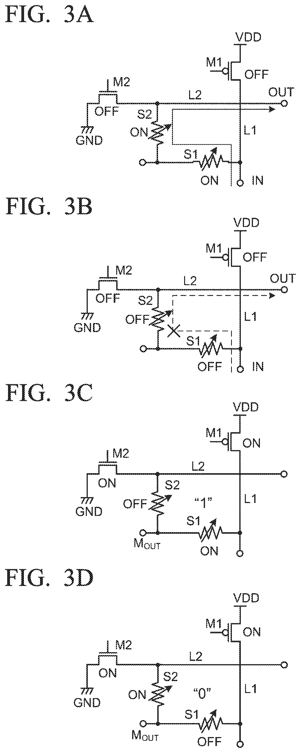
[0038] FIGS. 3A to 3D illustrate an example of operation of the reconfigurable circuit of this exemplary embodiment. In FIGS. 3A to 3D, it is assumed that switch elements SW1, SW2 are pMOS transistor M1 and nMOS transistor M2, respectively, and voltages V.sub.1, V.sub.2 are VDD and GND, respectively. Terminals T1 and T2 are input terminal IN and output terminal OUT for data routing, respectively. Terminal T3 is memory output terminal M.sub.OUT. In the data routing mode, a cutoff voltage and ground potential are applied to the gates of pMOS transistor M1 and nMOS transistor M2 to turn off them. As shown in FIG. 3A, when both NVRSs S1 and S2 are turned on (i.e., in ON-state), a signal can transmit from terminal IN to terminal OUT through NVRSs S1, S2. As shown in FIG. 3B, when both NVRSs S1 and S2 are turned off (i.e., in OFF-state), the path from terminal IN to terminal OFF is cut off. In the memory mode, data "1" is stored by turning on NVRS S1 and turning off NVRS S2, and data "0" is stored by turning off NVRS S1 and turning on NVRS S2. When data is read out, both transistors M1, M2 are turned on. FIG. 3C illustrates reading-out of data "1" in which voltage close to VDD appears at terminal M.sub.OUT. Fig. D illustrates reading-out of data "0" in which voltage close to GND appears at terminal M.sub.OUT.
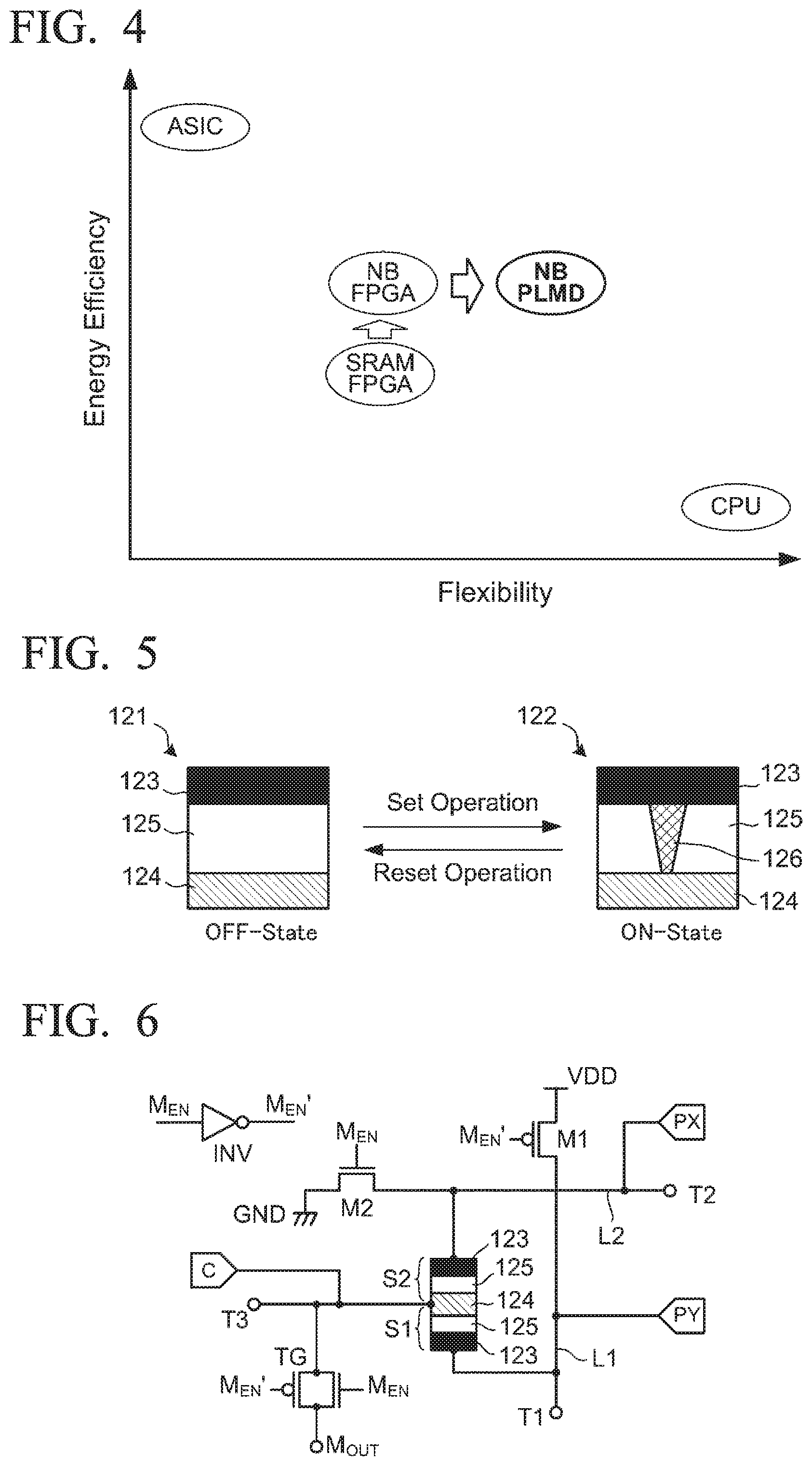
[0039] As described above, the present exemplary embodiment provides a novel reconfigurable circuit to implement both FPGA and a non-volatile memory using a single device for flexibility improvement. We name the novel reconfigurable circuit NBPLMD (Nanobridge.RTM. programmable logic memory device). FIG. 4 illustrates relationship between energy efficiency and flexibility of various semiconductor devices. As shown in FIG. 4, ASIC (Application Specific Integrated Circuit) has high energy efficiency and low flexibility while a CPU (Central Processing Unit) has low energy efficiency and high flexibility. SRAM FPGA has middle energy efficiency and middle flexibility. NBFPGA is an improved version in energy efficiency of SRAM FPGA. Our NBPLMD has flexibility higher than NBFPGA. Therefore, NBPLMD has well-balanced characteristics between energy efficiency and flexibility.
[0040] Next, NVRS which can be used in the reconfigurable circuit will be described. As described above, NVRS can be altered between ON-state (i.e., set state) and OFF-state (i.e., reset state). In FIG. 5, two NVRSs 121, 122 are illustrated, NVRS 121 is in OFF-state, and NVRS 122 is in ON-state. NVRS includes: active electrode 123 made of, for example, copper (Cu); inert electrode 124 made of, for example, ruthenium (Ru); and solid-electrolyte 125 sandwiched between active electrode 123 and inert electrode 124.
[0041] In the OFF-state, active electrode 123 and inert electrode 124 are electrically separated by solid-electrolyte 125, and the electric resistance between active electrode 123 and inert electrode 124 is very high. When the voltage of inert electrode 124 is fixed to zero and a positive voltage higher than a threshold voltage is applied to active electrode 123 of NVRS 121 in the OFF-state, metal ions are attracted by the electric field and supplied to solid-electrolyte 125. Then, metal bridge 126 is formed between active electrode 123 and inert electrode 124, and both electrode 123, 124 are electrically short-circuited by metal bridge 126. The resistance between active electrode 123 and inert electrode 124 is remarkably reduced. This operation making NVRS ON-state is referred to set operation. When the voltage of inert electrode 124 is fixed to zero and a negative voltage whose absolute value is larger than another threshold voltage is applied to active electrode 123 of NVRS 122 in the ON-state, metal ions in metal bridge 126 move in a direction of active electrode 123, and metal bridge 126 then disappears. The resistance between active electrode 123 and inert electrode 124 increases and returns the initial value, i.e., the value at the OFF-state. This operation making NVRS OFF-state is referred to reset operation. NVRS has high ON/OFF resistance ratio (typically, >10.sup.5) between the ON- and OFF-states. Small area overhead and high logic density can be achieved by replacing CMOS (Complementary MOS) switch with NVRS.
[0042] Two NVRSs are serially connected to constitute resistive switch assembly 111 in the present exemplary embodiment. Since each NVRS has active electrode 123 and inert electrode 124, there are four ways to serially connect two NVRSs. In order to improve reliability of the NVRSs, especially in the data routing mode, it preferable to connect the active electrodes of both NVRSs to each other, or connect the inert active electrodes of both NVRSs to each other. Two NVRSs in which the active electrodes of both NVRSs are connected to each other or the inert electrodes are connected to each other are called complementary NVRSs. When the inert electrodes of two NVRSs are connected each other, the two NVRSs can share a single inert electrode. In such a case, the coupling part of the two NVRSs is the shared inert electrode. Although the two NVRSs can similarly share a single active electrode, it is preferable to share the inert electrode in comparison with case of the shared active electrode from a viewpoint of compatibility with semiconductor fabrication processes.
[0043] FIG. 6 illustrates an example of the reconfiguration circuit with the shared inert electrode. Compared to the reconfigurable circuit shown in FIG. 2, the reconfigurable circuit shown in FIG. 6 differs in that NVRSs S1, S2 share inert electrode 124, and that circuits for programming and reading NVRSs S1, S2 are added. The program circuit is used both for programming the NVRSs for the data routing mode and for writing data to the NVRSs for the memory mode. As switch elements SW1, SW2, pMOS transistor M1 and nMOS transistor M2 are used, respectively. Memory enable signal M.sub.EN which is active during reading operation is supplied to the reconfigurable circuit and invertor INV generates reversed memory enable signal M.sub.EN' based on signal M.sub.EN. Shared inert electrode 124 functions as the coupling part between NVRSs S1, S2. Program drivers PX, PY are connected to lines L1, L2, respectively, and program driver C is connected to the coupling part of NVRSs S1, S2. The coupling part is also connected to memory output terminal M.sub.OUT through transmission gate TG to which signals M.sub.EN, M.sub.EN' are supplied. Transistors M1, M2 are configured to turn on when memory enable signal M.sub.EN is asserted. Transmission gate TG is also turned on when memory enable signal M.sub.EN is asserted. The operation of the circuit shown in FIG. 6 in the data routing mode and the memory mode are the same as those of the circuit shown in FIG. 2.
[0044] FIGS. 7A to 7D illustrate programming of NVRSs S1, S2 in the reconfigurable circuit shown in FIG. 6. Here, V.sub.SET is a voltage enough to change the state of NVRS from OFF-state to ON-state while V.sub.RESET is a voltage enough to change the state of NVRS from ON-state to OFF-state. It should be noted that application of voltage of V.sub.SET/2, i.e., half of V.sub.SET, does not cause the state change of NVRS, and application of V.sub.RESET/2 does not cause the change of NVRS. In order to simplify the programming operation, it is preferable that magnitude of V.sub.SET is equal to that of V.sub.RESET. Voltages V.sub.PX, V.sub.PY, V.sub.C are output voltages of program drivers PX, PY, C, respectively.
[0045] FIG. 7A illustrates the set operation for NVRS S1. In the initial stage, each of V.sub.PX, V.sub.PY, V.sub.C is maintained at level of V.sub.SET/2. Then, V.sub.C is changed to the ground potential GND and V.sub.PY is subsequently changed to V.sub.SET whereby the state of NVRS S1 shifts into the ON-state. After the transition to the ON-state, V.sub.PY is changed back to V.sub.SET/2 and V.sub.C is subsequently changed to V.sub.SET/2. V.sub.PX is unchanged throughout the set operation of NVRS S1. FIG. 7B illustrates the set operation for NVRS S2. The set operation of NVRS S2 is similar to the set operation of NVRS S1, but V.sub.PX is changed instead of V.sub.PY.
[0046] FIG. 7C illustrates the reset operation for NVRS S1. In the initial stage, each of V.sub.PX, V.sub.PY, V.sub.C is maintained at level of V.sub.RESET/2. Then, V.sub.C is changed to V.sub.RESET and V.sub.PY is subsequently changed to the ground potential GND whereby the state of NVRS S1 shifts into the OFF-state. After the transition to the OFF-state, V.sub.PY is changed back to V.sub.RESET/2 and V.sub.C subsequently is changed V.sub.RESET/2. V.sub.PX is unchanged throughout the reset operation of NVRS S1. FIG. 7D illustrates the reset operation for NVRS S2. The reset operation of NVRS S2 is similar to the reset operation of NVRS S1, but V.sub.PX is changed instead of V.sub.PY.
Second Exemplary Embodiment
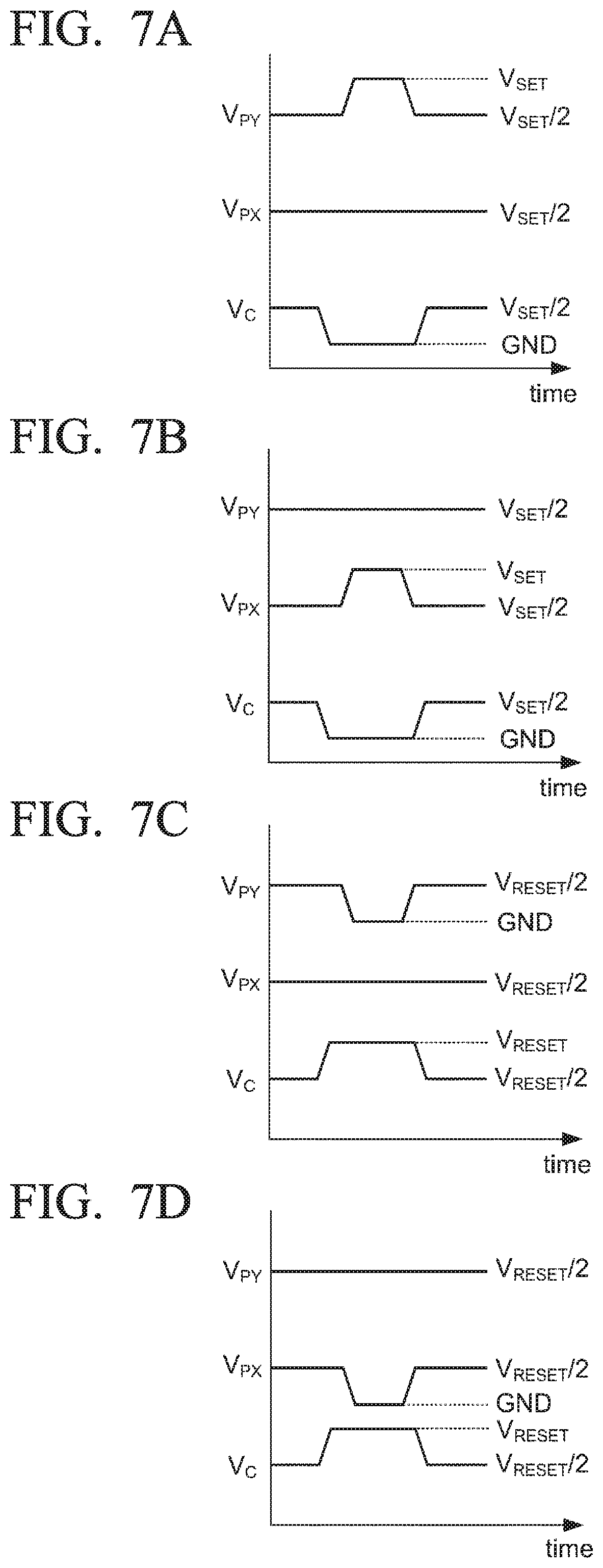
[0047] Next, applications of the above-mentioned reconfigurable circuit will be described. FIG. 8 illustrates the reconfigurable circuit according to the second exemplary embodiment in which a plurality of first lines and a plurality of second lines are arranged and the resistive switch assembly including two NVRSs serially connected to each other is disposed at each cross-point between the first lines and the second lines. In the drawing, the first lines extend in the vertical direction while the second lines extend in the horizontal direction. In the present embodiment too, each resistive switch assembly is a one-input-two-output NB (Nonobridge.RTM.) which is used both for a data routing switch between the first line and the second line, and for a memory cell.
[0048] In the example shown in FIG. 8, two first or vertical lines L.sub.V0, L.sub.V1 and two second or horizontal lines L.sub.H0, L.sub.H1 are arranged in a lattice manner and a resistive switch assembly or Nonobridge.RTM. is arranged at each cross-point between vertical lines L.sub.V0, L.sub.V1 and horizontal lines L.sub.H0, L.sub.H1, thereby constituting a 2.times.2 NB crossbar. Total eight NVRSs S1 to S8 are contained in the circuit shown in FIG. 8. Vertical lines L.sub.V0, L.sub.V1 are coupled to power source line VDD via pMOS transistors M11, M12, respectively. Horizontal lines L.sub.H0, L.sub.H1 are coupled to ground source line GND via nMOS transistors M21, M22, respectively. This NB crossbar can implement both a routing multiplexer (MUX) and a memory array and has different operational modes, data routing mode and memory mode. FIG. 9A and FIG. 9B illustrate the data routing mode and the memory mode of the circuit shown in FIG. 8, respectively.
[0049] In the data routing mode, transistors M11, M12, M21, M22 are cut off. It is assumed that ends of vertical lines L.sub.V0, L.sub.V1 are input ends IN0, IN1, respectively, and ends of horizontal lines L.sub.H0, L.sub.H1 are output ends OUT1, OUT2, respectively. As shown in FIG. 9A, to implement a data transfer path from IN0 to OUT0 and another data transfer path from IN1 to OUT1, NVRSs S3, S4, S7, S8 are made ON-state while the NVRSs S1, S2, S5, S6 are made OFF-state. The two NVRSs at the same cross-point have the same ON/OFF state.
[0050] In memory mode, one of two NVRSs at each cross-point is made ON-state and the other OFF-state to store logic value "1" or "0." In the example illustrated in FIG. 9B, NVRSs S1, S2 are made ON and OFF, respectively, to store logic value "1." NVRSs S3, S4 are made OFF and ON, respectively, to store logic value "0." NVRSs S5, S6 are similarly configured to store logic value "1" and NVRSs S7, S8 are configured to store logic value "0." When the stored values of the memory array are read, transistors M11, M12, M21, M22 are turned on. Then, the voltage of terminal T3 which is connected to the coupling part between the two NVRSs at each cross-point indicates the stored logic value. In this case, when the stored value is "0," the voltage of terminal T3 approaches to GND while the voltage of terminal T3 approached to VDD when the stored value is "1."
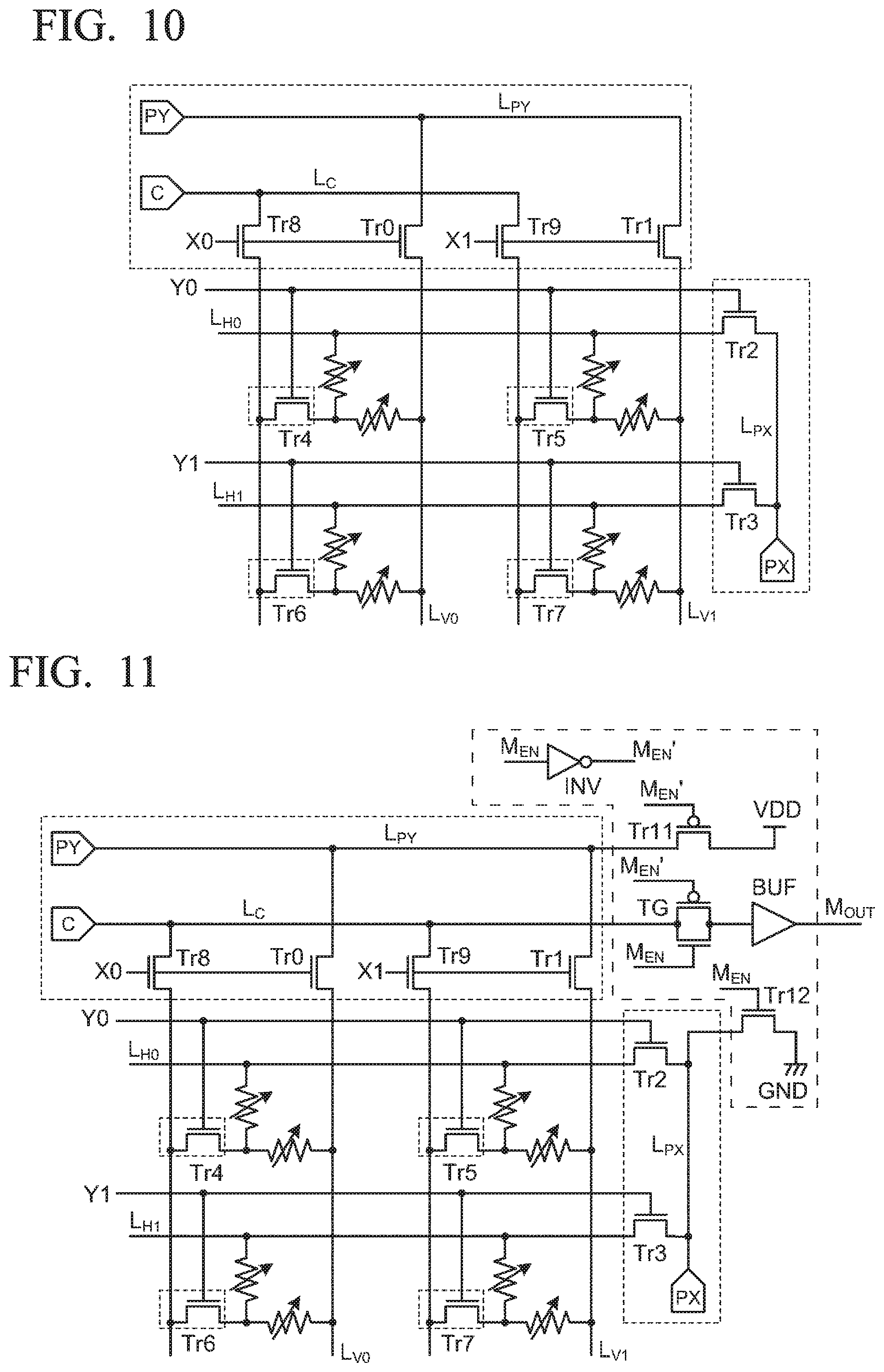
[0051] Programming of NVRSs in the reconfigurable circuit shown in FIG. 8 will be described. FIG. 10 illustrates a 2.times.2 NB crossbar in the related art which has only data routing function [NPL 2, PTL 1]. The circuit shown in FIG. 10 is equipped with a program circuit. Portions of the program circuit are surrounded by dashed lines in the drawing. Although the program circuit is used for separately programming NVRSs, the circuit shown in FIG. 10 does not implement a memory array. A control transistor is provided for each cross-point between the vertical lines and the horizontal lines. The source of the control transistor is connected to the coupling part between the two NVRSs at the same cross-point. In FIG. 10, nMOS transistors Tr4 to Tr7 are the control transistors at the respective cross-points. Diodes or the like may be used instead of the control transistors. Vertical lines L.sub.V0, L.sub.V1 are coupled to an output of a common column program driver PY via nMOS transistors Tr0, Tr1, respectively, and horizontal lines L.sub.H0, L.sub.H1 are coupled to an output of common row program driver PX via nMOS transistors Tr2, Tr3, respectively. The line connecting the output of column program driver PY to nMOS transistors Tr0, Tr1 is column program line L.sub.PY, and the line connecting the output of row program driver PX to nMOS transistors Tr2, Tr3 is row program line L.sub.PX. The drains of the control transistors on the same column are connected with each other, and then coupled to common mid program driver C via one of nMOS transistors Tr8, Tr9 which are provided for the respective columns. The line connecting the output of mid program driver C to nMOS transistors Tr8, Tr9 is mid program line L.sub.C. Row address signals X0, X1 and column address signals Y0, Y1 control nMOS transistors Tr0 to Tr9 for configuration of the NB crossbar.
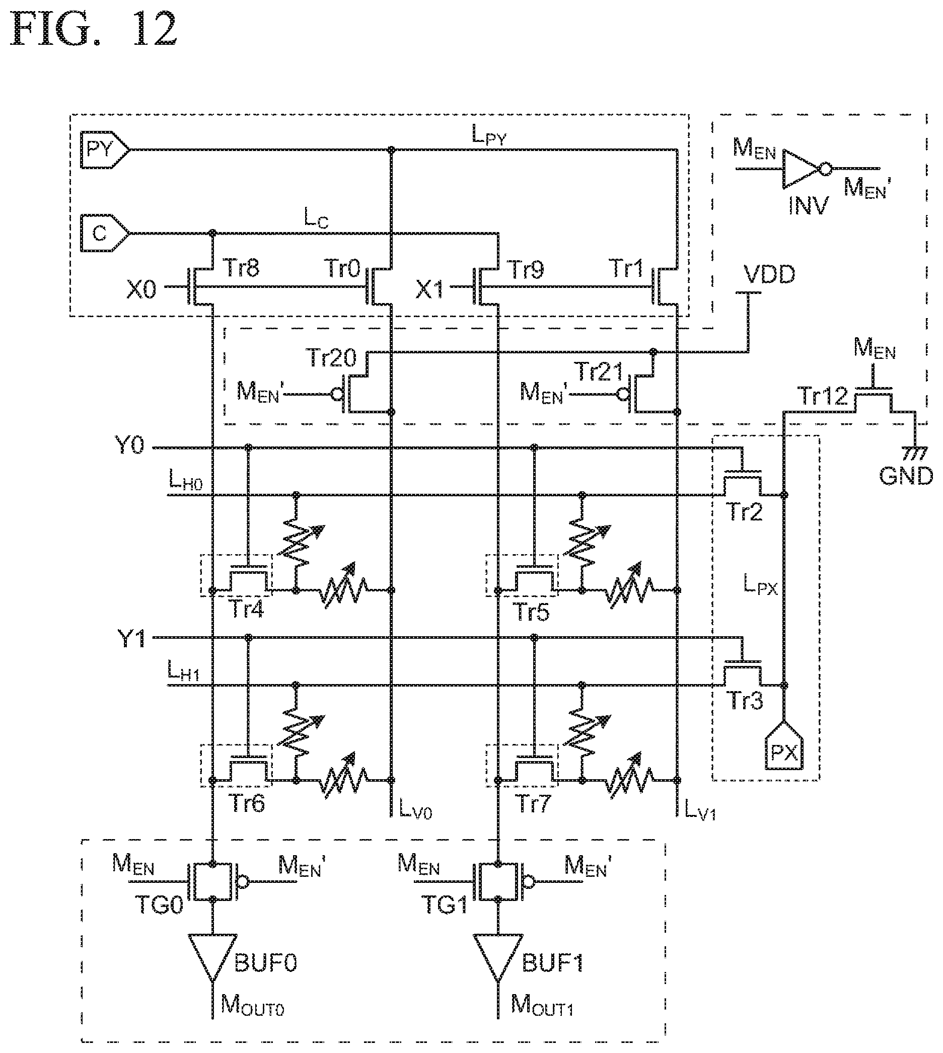
[0052] In order to realize the novel NB crossbar according to the second exemplary embodiment, which has both data routing function and memory function, we can add read circuits to the circuit of the related art shown in FIG. 10. FIG. 11 illustrates the reconfigurable circuit, i.e., NB crossbar, according to the second exemplary embodiment with a serial read circuit and the program circuit. The portions of the serial read circuit are surrounded by dashed-and-dotted lines while the portions of the program circuit are surrounded by dashed lines in the drawing.
[0053] In the example shown in FIG. 11, memory enable signal M.sub.EN, which is in High level when asserted, is supplied to the read circuit, and its inverse signal M.sub.EN' is generated by inverter INV. Power supply voltage VDD is applied to column program line L.sub.py via pMOS transistor Tr11 controlled by signal M.sub.EN'. Ground potential GND is applied to row program line L.sub.PX via nMOS transistor Tr12 controlled by signal M.sub.EN. Since the memory value is read from the coupling part of the two NVRSs of the same cross-point, the memory value is transferred to mid program line L.sub.C via the corresponding control transistor and one of nMOS transistors Tr8, Tr9. In order to supply the memory value to an external circuit, the mid program line is connected to buffer BUF via transmission gate TG controlled by signals M.sub.EN and M.sub.EN'. The output of buffer BUF is connected to memory output terminal M.sub.OUT.
[0054] For example, when data stored in the NVRSs at the cross-point of vertical line L.sub.V0 and horizontal line L.sub.H0 is read, it is necessary to set signal M.sub.EN as High, addresses X0, Y0 as High, and addresses X1, Y1 as low. Transistor Tr0 is turned on to apply power supply voltage VDD to vertical line L.sub.V0, and transistor Tr2 is turned on to apply ground potential GND to horizontal line L.sub.H0. Transistors Tr4, Tr8 are then turned on to output the data stored in the NVRSs at the target cross-point.
[0055] Ten transistors Tr0 to Tr9 constitute the program circuit shown in FIG. 11 and these transistors Tr0 to Tr9 also engage in the read operation. Additional components for the serial read circuit is only two transistors Tr11, Tr12, one invertor INV, one transmission gate TG and one buffer BUF. This leads to very small area overhead of the novel NB crossbar with both routing switch function and memory function compared with the NB crossbar of the related art which has only the routing switch function.
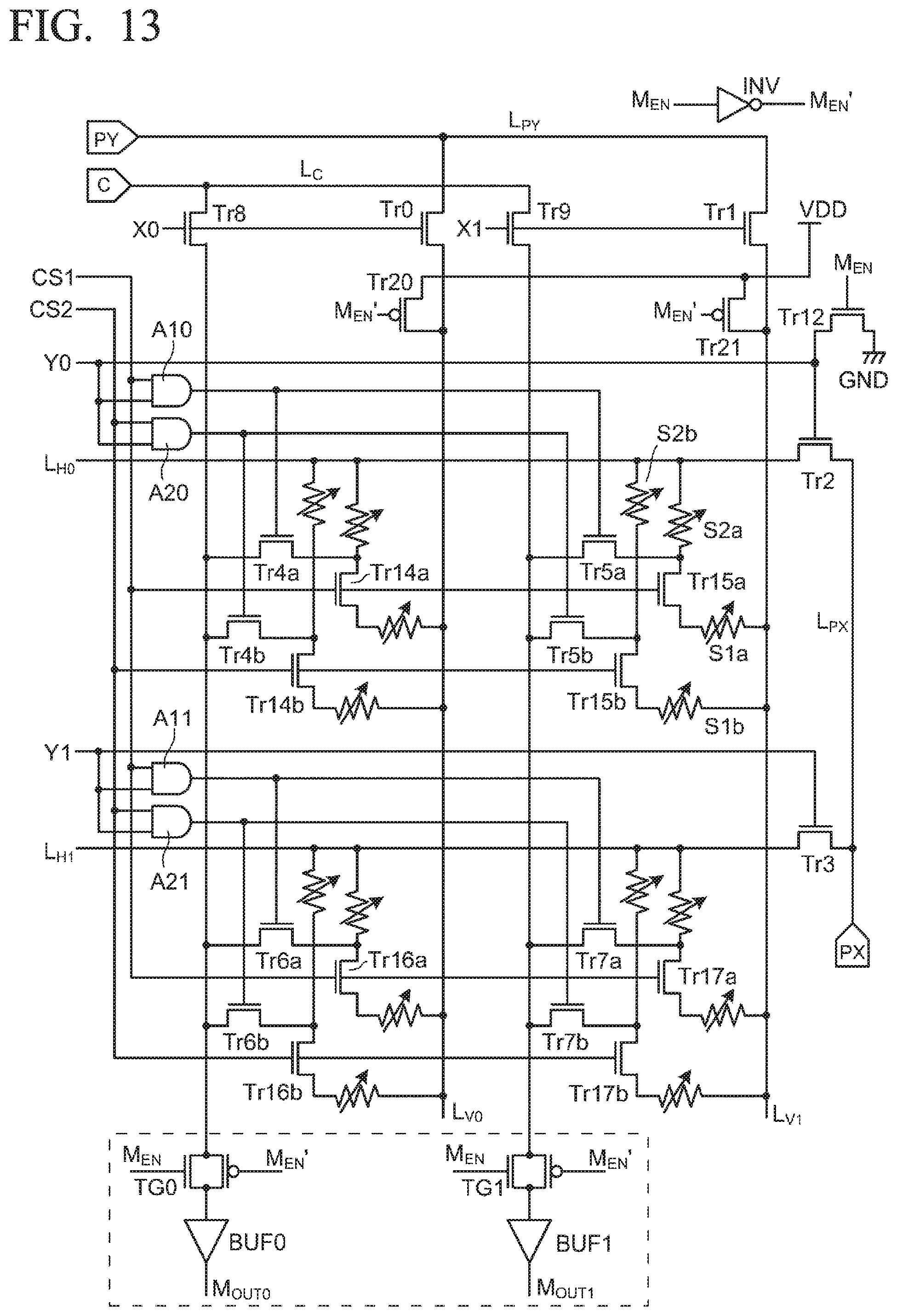
[0056] The NB crossbar shown in FIG. 11 includes the serial read circuit. When a high memory read rate is required, the serial read circuit can be replaced with a parallel read circuit. FIG. 12 illustrates a reconfigurable circuit with a program circuit and a parallel read circuit which is modification of the circuit shown in FIG. 11. The circuit shown in FIG. 12 is different from the circuit shown in FIG. 11 only in a parallel read circuit is used instead of the serial read circuit. The portions of the parallel read circuit are surrounded by dashed-and-dotted lines in FIG. 12.
[0057] In the parallel read circuit, invertor INV reverses memory enable signal M.sub.EN to generate signal M.sub.EN'. Vertical lines L.sub.V0, L.sub.V1 are connected to power source line VDD via pMOS transistors Tr20, Tr21, respectively. Transistors Tr20, Tr21 are controlled by signal M.sub.EN'. Ground potential GND is applied to row program line L.sub.PX via nMOS transistor Tr12 controlled by signal M.sub.EN. Transmission gates TG0, TG1 are provided for the respective columns. The drains of the control transistors on the same column are connected with each other, and then coupled to the corresponding one of transmission gates TG0, TG1. Each of transmission gates TG0, TG1 is controlled by signals M.sub.EN, M.sub.EN'. The outputs of transmission gates TG0, TG1 are connected memory output terminals M.sub.OUT0, M.sub.OUT1, via buffers BUF0, BUF1, respectively.
[0058] The circuit shown in FIG. 12 can read memory cells on the same row at the same time. When parallel reading is carried out, power source voltage VDD is applied, without using transistor Tr0, Tr1, to vertical lines L.sub.V0, L.sub.V1 via transistors Tr20, Tr21 controlled by signal M.sub.EN'. The memory data is supplied to the transmission gates and buffers for parallel read without using transistors Tr8, Tr9. For example, if the data stored in the NVRSs at the cross-point of vertical line L.sub.V0 and horizontal line L.sub.H0 and another data stored at the cross-point of vertical lines L.sub.V1 and horizontal line L.sub.H0 are read simultaneously, it is necessary to set signal M.sub.EN as High, address Y0 as High, and address Y1 as low. Signal M.sub.EN at High causes voltage VDD to be supplied to both vertical lines L.sub.V0, L.sub.V1. Ground potential GND is supplied to horizontal line L.sub.H0 because transistor Tr2 is turned on by address Y0. Transistors Tr4, Tr5 are turned on by address Y0, so that memory data corresponding to the cross-point of lines L.sub.V0, L.sub.H0 and another data corresponding to the cross-point of lines L.sub.V1, L.sub.H0 can be read to memory output terminals M.sub.OUT, M.sub.OUT1, simultaneously.
[0059] In the examples described above, two vertical lines L.sub.V0, L.sub.V1 and two horizontal lines L.sub.H0, L.sub.H1 are arranged to constitute a crossbar. However, each of the number of the vertical lines and the number of horizontal lines is not limited to two. Three or more vertical lines can be arranged and three or more horizontal lines can be arranged. The larger scale of the lattice structure of the vertical lines and the horizontal lines further improves flexibility of the reconfigurable circuit.
Third Exemplary Embodiment
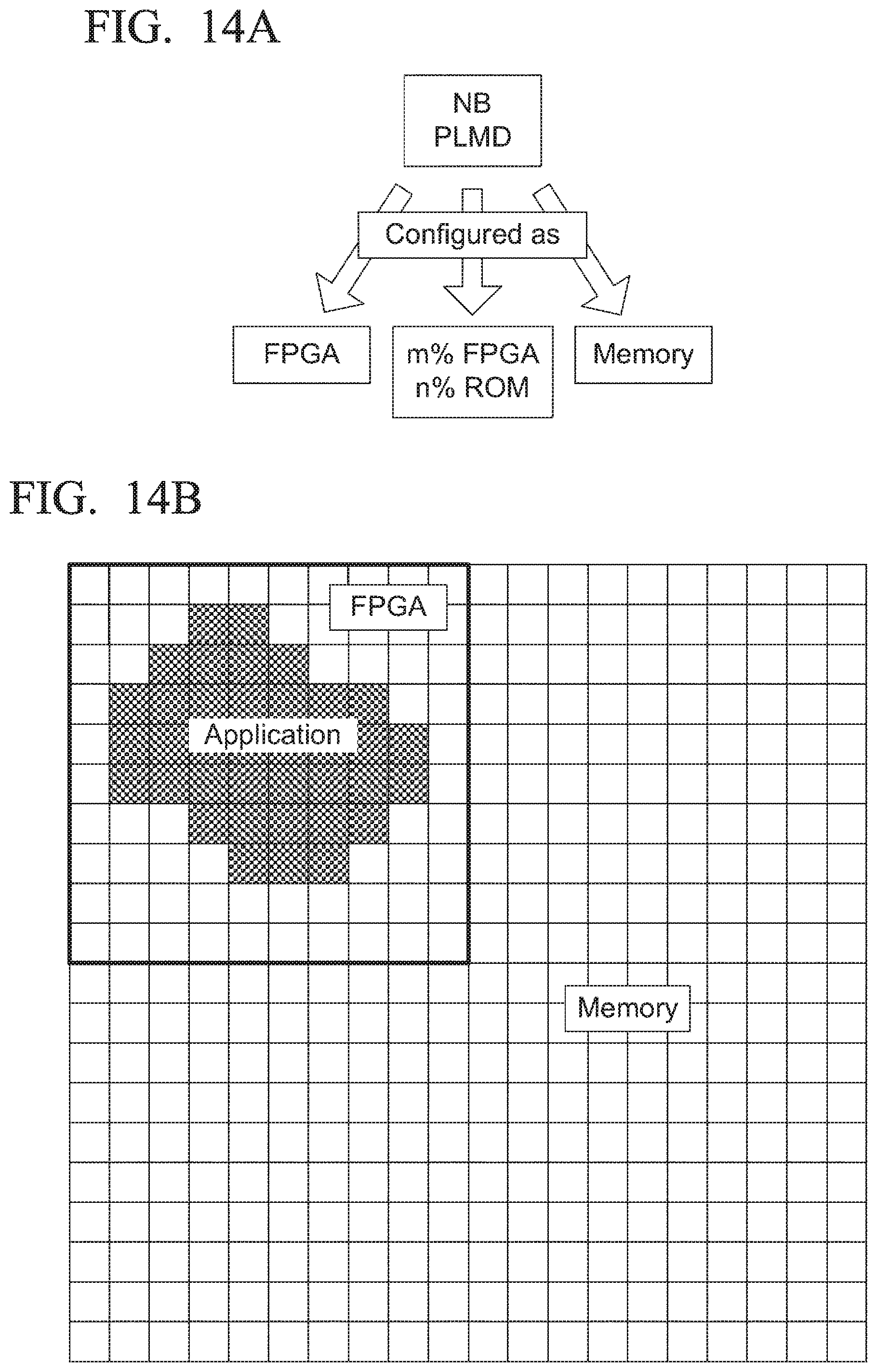
[0060] The reconfigurable circuit based on the present invention can be also applied to time-multiplexed crossbar or interconnect structures, such as proposed in [PTL 3], in which a plurality of switches are arranged at each of cross-points between horizontal lines and vertical lines and the switches are selected in time-divisional manner such that two or more switches are not simultaneously selected. The time-multiplexed crossbar achieves time-divisional changeover of contexts in FPGA. The selection of the switches is performed by using a pass transistor interposed in each switch. Time control signals are applied to the respective pass transistors at each cross-point. Since the selection using the pass transistor can be rapidly executed, the time-multiplex crossbar configuration provides runtime-changeable data signal routing which improves flexibility of FPGA.
[0061] FIG. 13 illustrates an example of a reconfigurable circuit according to a third exemplary embodiment in which a plurality of resistive switch assemblies each comprising two NVRSs serially-connected to each other are arranged at each cross-points between the vertical lines and the horizontal lines. The example shown in FIG. 13 is a modification of the circuit shown in FIG. 12 and is thus equipped with two resistive switch assemblies at each cross-point between two vertical lines L.sub.V0, L.sub.V1 and two horizontal lines L.sub.H0, L.sub.H1. However, three or more vertical lines and three or more horizontal lines can be arranged. In addition, although two resistive switch assemblies are arranged at each cross-point, the number of resistive switch assemblies per cross-point between the first lines, i.e., the vertical lines, and the second lines, i.e., the second lines, can be three or more. The multiplicity of contexts which are switched in a time-divisional manner increases as the number of resistive switch assemblies per cross-point increases.
[0062] A pass transistor is arranged in each of the resistive switch assemblies such that the pass transistor can interrupt the current flowing through the serially-connected two NVRSs in the resistive switch assembly. In FIG. 13, two resistive switch assemblies arranged at the cross-point of vertical line L.sub.V1 and horizontal line L.sub.H0, the first assembly including two NVRSs S1a, S2a and pass transistor Tr15a, and the second assembly including two NVRSs S1b, S2b and pass transistor Tr15b. In the first resistive switch assembly, the second ends of NVRSs S1a, S1b are connected to lines L.sub.V1, L.sub.H0, respectively, and pass transistor Tr15a which is a nMOS transistor is inserted between the first ends of NVRSs S1a, S2a. The source of control transistor Tr5a is connected to the junction between first end of NVRS S2a and pass transistor Tr15a. Similarly, in the second resistive switch assembly, the second ends of NVRSs S1b, S2b are connected to lines L.sub.V1, L.sub.H0, respectively, and pass transistor Tr15b is inserted between the first ends of NVRSs S1b, S2b. Control transistor Tr5b is connected to the junction between first end of NVRS S2b and pass transistor Tr15b. The drains of control transistors Tr5a, Tr5b are commonly connected to the drains of the other control transistors Tr7a, Tr7b in the same column, and then connected to transistor Tr9 which is controlled by address X1.
[0063] Two time control signals CS1, CS2 are supplied to the reconfigurable circuit. Signal CS1 is applied to the gates of pass transistors Tr14a, Tr15a, Tr16a, Tr17a which are included in the first resistive switch assemblies at the respective cross-point. Signal CS2 is applied to the gates of pass transistors Tr14b, Tr15b, Tr16b, Tr17b which are included in the second resistive switch assemblies at the respective cross-point. In addition, AND gate A10 receives time control signal CS1 and address Y0, and the output of AND gate A10 is supplied to the gates of controls transistors Tr4a, Tr5a in the first resistive assemblies on horizontal line V.sub.H0. Similarly, AND gate A20 receives time control signal CS2 and address Y0, and the output of AND gate A20 is supplied to the gates of controls transistors Tr4b, Tr5b in the second resistive assemblies on horizontal line V.sub.H0. With regard to vertical line V.sub.H1, two AND gates A11, A21 are similarly provided and their outputs are supplied to the gates of control transistors Tr6a, Tr7a, Tr6b, Tr7b.
[0064] Although the pass transistor is inserted between the first ends of the first NVRS and the second NVRS for each cross-point in the example shown in FIG. 12, the position of the pass transistor is not limited to this. The pass transistor can be disposed at an arbitrary position between the coupling position of the first NVRS to the first line and the coupling position of the second NVRS to the second line. For example, in the case of the cross-point of vertical line L.sub.V1 and horizontal line L.sub.H0 shown in FIG. 12, pass transistor Tr15a may be inserted between vertical line L.sub.V1 and the second end of NVRS S1a. Alternatively, pass transistor Tr15a may be inserted between horizontal line L.sub.H0 and the second end of NVRS S2a.
[0065] The operation of the reconfigurable circuit shown in FIG. 13 is the same as that of the circuit shown in FIG. 12 except for selection of one of two resistive switch assemblies at each cross-point by time control signals CS1, CS2. When the first resistive switch assemblies or NBs are used for data routing switches or memory cells, time control signal CS1 is activated while time control signal CS2 is kept inactive. On the other hand, if the second resistive switch assemblies are used for data routing switches or memory cells, time control signal CS2 is activated while time control signal CS1 is kept inactive. The programming operation to the NVRSs is also carried out by activating one of time control signals CS1, CS2.
Fourth Exemplary Embodiment
[0066] Next, a fourth exemplary embodiment according to the present invention will be explained. As described above, the reconfigurable circuits of the above exemplary embodiments are called as NBPLMD. The present exemplary embodiment explains how to use the novel NBPLMD. FIGS. 14A and 14B illustrate usage of the novel NBPLMD. The NBPLMD has the same structure as the previous NBFPGA shown in FIG. 1, but with the novel NB crossbar which can be used for both a data routing switch and a memory, as disclosed in the above exemplary embodiments. As shown in FIG. 14A, there are three kinds of usage for the NBPLMD. The first one is that the NBPLMD is configured as a complete NBFPGA if a large-sized application is mapped on the NBPLMD. The second one is that the NBPLMD is configured as a complete memory if only data storage is necessary. The third one is that one part of the NBPLMD is configured as NBFPGA and the other part is configured as a memory if both application and memory are necessary simultaneously. The example shown in FIG. 14B illustrates the case where an application can be realized using 25% of the NBPLMD, the other 75% can be used as a programmable ROM (read only memory). The area ratio between the NBFPGA part and the memory part can be arbitrarily set between the ranges of 1:0 and 0:1. Since the data routing mode, i.e., NBFPGA mode, and the memory mode are different only in the state of memory enable signal M.sub.EN and data pattern written to the serially connected two NVRSs in each NB, the mode of NBPLMD can be dynamically change between the NBFPGA mode and the memory mode for each block in the NBPLMD during the operation of the NBPLMD.
[0067] FIG. 15 illustrates how a large size FPGA or memory can be provided by NBPLMD with a typical architecture. In this example, it is assumed that cluster size, segment length and segment lane are optimized to be 4 as introduced in [NPL 3], and a cell array of 64.times.64 cells are arranged in NBPLMD. Each cell has four look-up tables (LUTs), therefore totally 64.times.64.times.4=16384 LUTs are provided in the FPGA mode of the NBPLMD. As shown in FIG. 15, each cell of NBPLMD has thirty-two (32) horizontal lines L.sub.H0 to L.sub.H31 and sixty-nine (69) vertical lines L.sub.V0 to L.sub.V68, therefore a 32.times.69 NB crossbar is formed per cell. In the memory mode, since 32.times.69.times.64.times.64=9,043,968, a 9-megabits memory is provided by the NBPLMD.
[0068] The reconfigurable circuits of the above exemplary embodiments may be used in, for example, mobile phones, IoT (Internet of Things) devices, and so on. A highly flexible PLMD (programmable logic memory device) can be realized by the reconfigurable circuits described above.
[0069] It is apparent that the present invention is not limited to the above exemplary embodiments and examples, but may be modified and changed without departing from the scope and sprit of the invention.
REFERENCE SIGNS LIST
[0070] 111 Resistive switch assembly, [0071] L1, L2 lines, [0072] S1, S2 Non-volatile resistive switches (NVRSs), [0073] T1, T2, T3 Terminals.
* * * * *
D00000
D00001
D00002
D00003
D00004
D00005
D00006
D00007
D00008
D00009
D00010
XML
uspto.report is an independent third-party trademark research tool that is not affiliated, endorsed, or sponsored by the United States Patent and Trademark Office (USPTO) or any other governmental organization. The information provided by uspto.report is based on publicly available data at the time of writing and is intended for informational purposes only.
While we strive to provide accurate and up-to-date information, we do not guarantee the accuracy, completeness, reliability, or suitability of the information displayed on this site. The use of this site is at your own risk. Any reliance you place on such information is therefore strictly at your own risk.
All official trademark data, including owner information, should be verified by visiting the official USPTO website at www.uspto.gov. This site is not intended to replace professional legal advice and should not be used as a substitute for consulting with a legal professional who is knowledgeable about trademark law.