Printed Circuit Board Mounting Arrangement
DIACONU; DORIN
U.S. patent application number 16/652711 was filed with the patent office on 2020-09-17 for printed circuit board mounting arrangement. The applicant listed for this patent is VITESCO TECHNOLOGIES GMBH. Invention is credited to DORIN DIACONU.
| Application Number | 20200295481 16/652711 |
| Document ID | / |
| Family ID | 1000004881198 |
| Filed Date | 2020-09-17 |

| United States Patent Application | 20200295481 |
| Kind Code | A1 |
| DIACONU; DORIN | September 17, 2020 |
PRINTED CIRCUIT BOARD MOUNTING ARRANGEMENT
Abstract
A printed circuit board mounting arrangement, in particular for use in environments with an aggressive vibration profile such as a motor vehicle, includes a housing and a circuit board secured to a connector body by mechanical press fit pins extending through location holes on a flange formed on the connector body to the printed circuit board. The arrangement provides for a secure connection that can achieve a high IP rating.
| Inventors: | DIACONU; DORIN; (MUENCHEN, DE) | ||||||||||
| Applicant: |
|
||||||||||
|---|---|---|---|---|---|---|---|---|---|---|---|
| Family ID: | 1000004881198 | ||||||||||
| Appl. No.: | 16/652711 | ||||||||||
| Filed: | September 28, 2018 | ||||||||||
| PCT Filed: | September 28, 2018 | ||||||||||
| PCT NO: | PCT/EP2018/076443 | ||||||||||
| 371 Date: | April 1, 2020 |
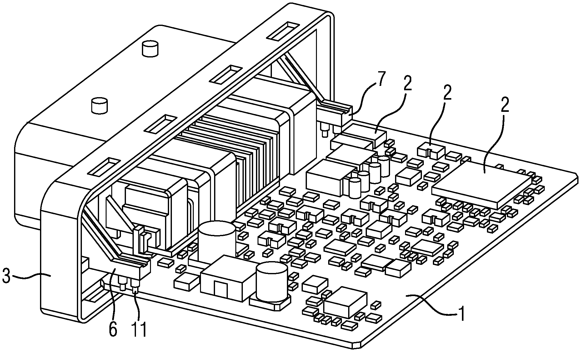
| Current U.S. Class: | 1/1 |
| Current CPC Class: | H05K 5/0069 20130101; H01R 12/7064 20130101; H01R 12/585 20130101; H01R 2201/26 20130101 |
| International Class: | H01R 12/70 20060101 H01R012/70; H01R 12/58 20060101 H01R012/58; H05K 5/00 20060101 H05K005/00 |
Foreign Application Data
| Date | Code | Application Number |
|---|---|---|
| Oct 10, 2017 | EP | 17465560 |
Claims
1-6. (canceled)
7. A printed circuit board mounting arrangement for use in an environment with an aggressive vibration profile, the printed circuit board mounting arrangement comprising: a housing; a connector body configured to cooperate with said housing, said connector body having at least one flange, said at least one flange having a location hole formed therein; a printed circuit board configured to be received by said housing to form a closed assembly, said printed circuit board having a location hole formed therein corresponding to said location hole formed in said at least one flange; and at least one mechanical press fit pin received in said location hole formed in said at least one flange and in said location hole formed in said printed circuit board to provide a mechanical connection between said connector body and said printed circuit board.
8. The printed circuit board mounting arrangement according to claim 7, wherein: said at least one flange of said connector body includes first and second flanges; said location hole formed in said at least one flange includes at least one respective location hole formed in each of said flanges; and said at least one press fit pin includes a plurality of press fit pins each being received in a respective one of said location holes formed in said flanges in an installed position.
9. The printed circuit board mounting arrangement according to claim 7, wherein said housing includes an interior wall, and first and second rails formed on said interior wall, said rails being configured to receive said printed circuit board and to substantially retain said printed circuit board in place.
10. The printed circuit board mounting arrangement according to claim 7, wherein said housing has one or more webs having a cutout formed therein for receiving said printed circuit board and substantially retaining said printed circuit board in place.
11. The printed circuit board mounting arrangement according to claim 9, wherein said housing has one or more webs having a cutout formed therein for receiving said printed circuit board and substantially retaining said printed circuit board in place.
12. The printed circuit board mounting arrangement according to claim 7, wherein said connector body includes at least one bracket on which said at least one flange is formed.
13. The printed circuit board mounting arrangement according to claim 7, wherein said connector body includes a push fit connector adapted to rigidly connect said connector body to said housing.
Description
[0001] The invention relates to a printed circuit board mounting arrangement in a housing, in particular, but not exclusively, for use in environments with an aggressive vibration profile such as a motor vehicle.
[0002] Many systems in motor vehicles are controlled by means of electronic control units. These devices comprise electronic components, in particular sensors for the detection of physical parameters such as accelerometers, which are used in diverse applications such as airbag controls and stability control systems. If the electronic control unit determines that the accelerometer output is outside a certain parameter range, a control signal is produced to, for example, activate the airbag or stability control.
[0003] For the installation of the electronic components in the vehicle interior, the electronic control unit typically comprises a housing in which a printed circuit board with electronic components mounted thereon is positioned. The housing is provided with a connection unit, which connection electrically contacts the carrier and as a result, the electronic components on the carrier. The control unit can be connected to a system to be controlled via the connection.
[0004] As in use the vehicle engine will generate vibrations in the vehicle chassis, steps are taken to reduce the effects of such vibration on the printed circuit board components. In order to ensure a vibration-free mounting of the printed circuit board in the housing of the control device and thus an unadulterated signal transmission, circuit boards with self-tapping or cutting mounting screws, which are rotated into the housing, have been used widely. Other types of fastening of the circuit board are, for example, the caulking of the printed circuit board in the housing via plastic pins and hot gas rivets. In addition, it is known to effect a fastening of printed circuit boards in the housing by means of clamping springs.
[0005] DE 10 2008 037 278 discloses a device which has a mount designed as a printed circuit board (PCB), where an assembly of electronic components containing a sensor is placed in the mount. A connection unit connects the device to an electronic system to be controlled. The mount with the electronic components assembly is arranged in the housing. The housing, the connection unit and the mount are mechanically fixed in a stiffening frame at a region of the sensor using screws, where the device is mechanically mounted on a mounting surface. The device disclosed in this document suffers from an additional problem in that the electrical pins are occasionally bent during mounting and so the assembly process is expensive.
[0006] All electronic control devices known from the prior art suffer from the problem that the transmission of vibrations to the printed circuit board cannot be effectively prevented. In particular, vibrations can occur in the region of the sensor and lead to a falsification of measuring signals and thus, under certain circumstances, to a fault behavior of the system to be controlled.
[0007] The known solutions suffer from the additional problem that during the assembly process of the connector into the housing, the forces that act on the header can cause stress to the electrical connection pins.
[0008] It is an object of the present invention to provide a circuit board mounting arrangement with a connector that is less liable to produce stress on the connection pins during the installation process
[0009] This object is achieved with a circuit board mounting arrangement having the features of claim 1. Further preferred or advantageous embodiments and developments are specified in the sub-claims, the following description and the drawings.
[0010] A printed circuit board mounting arrangement for use in an environment with an aggressive vibration profile is disclosed according to one aspect. The printed circuit board mounting arrangement can also be denoted as a printed circuit board mounting assembly. It comprises a connector body having a flange, which flange is provided with a location hole. It further comprises a printed circuit board being provided with a corresponding location hole. In addition, it comprises a mechanical press fit pin providing a mechanical connection between the connector and the printed circuit board, wherein the connector body is configured to co-operate with a housing, which housing receives the printed circuit board to form a closed assembly. For providing the mechanical connection, the press fit pin is in particular received in the location hole of the flange. It may expediently also be received in the corresponding location hole of the printed circuit board.
[0011] In particular, the flange extends across a portion of the length of the printed circuit board. The flange may expediently project at a side of the connector body facing towards the PCB and in a direction parallel to a main extension plane of the PCB.
[0012] According to a further aspect, the present disclosure relates to a printed circuit board mounting in a housing, in particular, for use in environments with an aggressive vibration profile such as a motor vehicle. The circuit board is secured to a connector body by means of mechanical press fit pins extending through location holes on a flange formed on the connector to the printed circuit board.
[0013] The solution according to the present disclosure has the ad-vantage that the printed circuit board can be rigidly mounted so that there is no flutter on the board even in locations with an aggressive vibration profile such as the wheel arch of a vehicle. The solution can also be mounted in a one step process, in contrast to the prior art solution which had a two part construction process, with a much reduced likelihood of electrical pin damage.
[0014] The arrangement may provide for a secure connection that can achieve a high IP rating. In particular, the arrangement of the invention may advantageously dispense with soldering in the fastening, which reduces the fumes produced in the production process and the quantity of toxic compounds in the device whilst enabling a higher IP rating.
[0015] According to one embodiment, the connector body is provided with first and second flanges, each of which flanges is provided with at least one location hole, each of which location holes receives a press fit pin in the installed position. Expediently, the PCB may comprise a plurality of corresponding location holes, each corresponding location hole of the PCB being assigned to one of the location holes of the first and second flanges. For example, each of the first and second flanges comprises at least two location holes, receiving first and second press fit pins, respectively. In one development, the first and second press fit pins are
[0016] The printed circuit board mounting arrangement may further comprise the housing according to some embodiments. In one embodiment, the housing is provided with first and second rails formed on an interior wall, which rails are configured to receive the printed circuit board and to substantially retain the printed circuit board in position. In a further embodiment, the housing is provided with one or more webs having a cut out to receive the printed circuit board and to substantially retain the printed circuit board in position.
[0017] In one embodiment, the connector is provided with a bracket, on which bracket the flanges are formed.
[0018] In one embodiment, the connector is provided with a push fit connector which is operable to rigidly connect the connector to the housing.
[0019] An exemplary embodiment of the invention will now be described in greater detail with reference to the drawings in which
[0020] FIG. 1 shows a perspective view of a PCB mounting arrangement according to an exemplary embodiment;
[0021] FIG. 2 shows a side view partially in cross section of the PCB mounting arrangement;
[0022] FIG. 3 shows a perspective view of the housing into which the PCB is mounted;
[0023] FIG. 4 shows the printed circuit board and connector body immediately prior to insertion in the housing.
[0024] FIG. 1 shows a perspective view of a printed circuit board mounting arrangement according to an exemplary embodiment of the invention. It comprises a printed circuit board (PCB) 1 having a plurality of components 2 mounted thereon and a connector arrangement for the printed circuit board 1. The printed circuit board 1 is mounted on a connector body 3 of the connector arrangement, which connector body 3, in use, is connected to a housing for the printed circuit board 1. The printed circuit board 1 is provided with--in particular drilled--holes 4 which receive electrical pins 5 to provide the electrical connection to the vehicle communication bus.
[0025] First and second brackets 6, 7 are provided at opposed edges of the connector body. Each bracket comprises a triangular form with the opposite end attached to the connector body and the end adjacent to the printed circuit board 1 being provided with a grooved flange 8 extending a short distance across the length of the printed circuit board 1. The brackets 6, 7 with the flanges 8 project at a side of the connector body 3 which faces towards the PCB 1, opposite of the side of the connector body 3 which is provided for engaging with a mating connector.
[0026] The flange 8 is provided with two location holes 9 and the printed circuit board 1 is provided with two corresponding location holes 10. Mechanical press fit pins 11 are provided in each corresponding hole pair 9, 10 to provide a mechanical rather than an electrical connection between the bracket 6, 7 and the printed circuit board 1. The pins 11 are adapted to transfer the pressure applied on the connector body during the assembly process of the PCB arrangement with the housing. The two pins 11 are connected by and preferably in one piece with a web extending laterally between the pins 11. The web is sandwiched between the flange 8 and the PCB 1. The press fit pins 11 may be electrically insulated from all conductor tracks of the PCB or grounded in this and other embodiments. It is also conceivable that the press fit pins 11 are made from an insulating material in this or other embodiments, for example from plastic.
[0027] The press fit pins 11 both fix and orientate the printed circuit board 1 during the initial press fit process and eliminate the possibility of deformation of the electrical pins caused by the application of forces on the support structure perpendicular to the connector that might otherwise arise. The fixing process can be performed in a single step without additional production steps. The mechanical press fit connection enables screws to be dispensed with, which advantageously enables the use of a closed housing. The use of a closed housing enables the device to achieve a higher IP rating than has been possible before and so the housing can be installed in places subject to aggressive environmental media such as a vehicle wheel arch.
[0028] FIG. 2 shows a side view partially in cross section of the connector arrangement with the printed circuit board 1 attached to the connector 3. The printed circuit board is provided with components 2 and drilled holes 4 which receive electrical pins 5. The brackets 6, 7 and flanges 8 extend laterally from the connector 3 and are provided with location holes 9. Press fit pin 11 is inserted through the location hole 9 and into and through a corresponding hole 10 on the printed circuit board. The electrical pins 5 also extend through the circuit board to provide the electrical connection from the connector body to the printed circuit board.
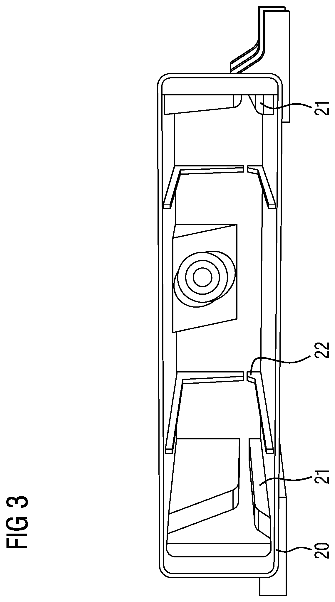
[0029] FIG. 3 shows a perspective view of the interior of the housing 20 into which the printed circuit board is mounted. The housing 20 has a rectangular opening defined by two lateral walls parallel to the surface of the printed circuit board in the installed position and two walls perpendicular to the printed circuit board. Two rails 21 are formed on the interior of the perpendicular walls, which rails have an opening adapted to facilitate the insertion of the printed circuit board during assembly but which narrows towards the rear wall of the housing so that the printed circuit board is held in position by the rails on the side wall. The rear interior wall of the housing is provided with two substantially vertical webs 22 that have a small cut out adapted to receive and substantially retain the printed circuit board in the installed position. The housing is further provided with mounting points on its exterior so that it can be screwed or bolted to a vehicle. A valve is provided to enable air to enter and exit the housing once it is assembled. The printed circuit board is therefore retained on each of its edges and so is able to be used in significantly more aggressive vibratory environments such as in the vicinity of a vehicle wheel arch.
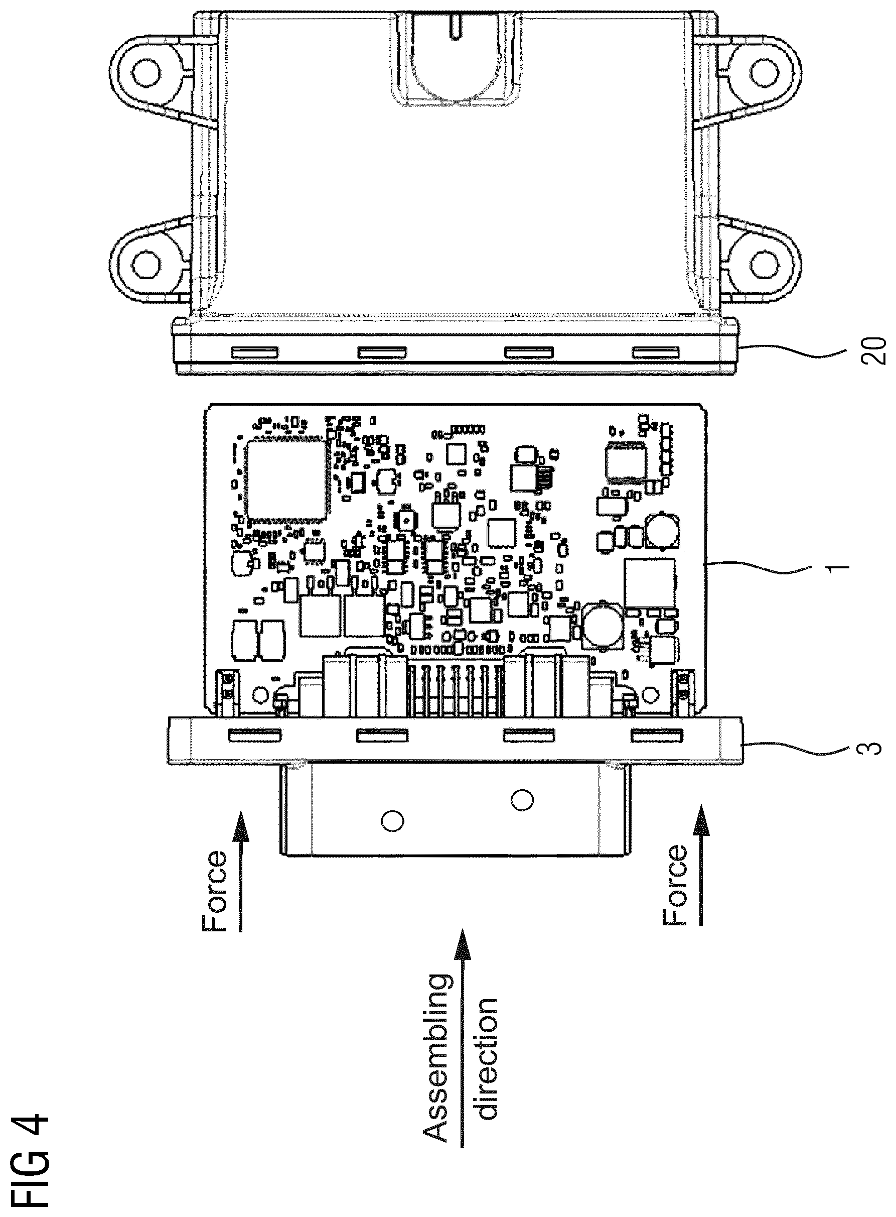
[0030] FIG. 4 shows the printed circuit board 1 and connector body 3 immediately prior to insertion in the housing 20. The connector body is provided with a series of resilient clips adapted to engage in corresponding elements on the housing 20 to fix the printed circuit board and connector in position in the housing, which can then be mounted in a vehicle. The connector arrangement advantageously can be assembled in a single process by a robot. The robot does not need to press the printed circuit board against the housing as part of the assembly. The assembly process is therefore lower cost and also has a lower likelihood of the printed circuit board being damaged either during the assembly process or due to flutter caused by vibration when installed in a vehicle.
* * * * *
D00000
D00001
D00002
D00003
XML
uspto.report is an independent third-party trademark research tool that is not affiliated, endorsed, or sponsored by the United States Patent and Trademark Office (USPTO) or any other governmental organization. The information provided by uspto.report is based on publicly available data at the time of writing and is intended for informational purposes only.
While we strive to provide accurate and up-to-date information, we do not guarantee the accuracy, completeness, reliability, or suitability of the information displayed on this site. The use of this site is at your own risk. Any reliance you place on such information is therefore strictly at your own risk.
All official trademark data, including owner information, should be verified by visiting the official USPTO website at www.uspto.gov. This site is not intended to replace professional legal advice and should not be used as a substitute for consulting with a legal professional who is knowledgeable about trademark law.